Note: Descriptions are shown in the official language in which they were submitted.
CA 02912240 2015-11-17
EMERGENCY LIGHTING BATTERY CHARGER
BACKGROUND
Fluorescent lamps use phosphors excited by electrons to create light.
Fluorescent lamps
ionize mercury vapor in a glass tube which causes electrons in the gas to emit
photons at
ultraviolet (UV) frequencies. The UV light is converted into visible light
using a phosphor
coating on the inside of the glass tube. The most common fluorescent lamp is a
hot cathode
lamp. A hot cathode lamp includes a glass tube filled with an inert gas (e.g,
argon) at low
pressure. An electrode is located on each side of the glass tube. A ballast
regulates alternating
current (AC) power that is applied to the electrodes. In certain applications
where light from
fluorescent lamps may be required even during power outages, power supplies
with battery
back-up have been implemented to power the lamps during power outages. Nickel
Cadmium (NiCad) batteries are typically used in fluorescent light back-up
power supplies.
BRIEF DESCRIPTION OF THE DRAWINGS
FIG. 1 is a diagram that illustrates an overview of an exemplary emergency
lighting
fluorescent power supply that may be used, in conjunction with an external
ballast, for
powering a fluorescent light;
FIG. 2 is a diagram that depicts an exemplary implementation of the
fluorescent power
supply of FIG. 1;
FIG. 3 is a diagram that depicts details of the circuitry of an exemplary
implementation of the
battery charger of FIG. 2;
FIG. 4 is a diagram that depicts details of an exemplary implementation of the
double rate
charger control circuitry of FIG. 2;
FIG. 5 is a diagram that depicts details of an exemplary implementation of the
relay coils of
FIG. 2 as connected to the rechargeable battery;
FIG. 6 is a diagram that depicts details of the circuitry of an exemplary
implementation of the
high frequency inverter circuitry/ballast AC output circuitry and impedance
network of
- 1 -
CA 02912240 2015-11-17
FIG. 2;
FIG. 7 is a diagram that depicts details of an exemplary interconnection of
the relay contacts
with the external AC ballast and with the fluorescent power supply of FIG. 2;
FIG. 8 is a diagram that depicts details of an exemplary implementation of the
AC ballast
control circuitry of FIG. 2;
FIG. 9 is a diagram that depicts details of an exemplary implementation of the
controller of
FIG. 2, and its associated circuitry;
FIG. 10 is a diagram that depicts an overview of the powering of the
fluorescent light from
the AC ballast or fluorescent power supply of FIG. 1; and
FIGs. 11-13 are flow diagrams that illustrate an exemplary process for the
fluorescent power
supply to charge a rechargeable battery using a selected one of at least two
different charging
rates for selected charging periods.
DETAILED DESCRIPTION OF PREFERRED EMBODIMENTS
The following detailed description refers to the accompanying drawings. The
same reference
numbers in different drawings may identify the same or similar elements. The
following
detailed description does not limit the invention.
Emergency fluorescent lights, which are powered by back-up batteries during
power outages,
require battery recharges to maintain the back-up batteries in operable
condition. Underwriter
Laboratories (UL) rules require that rechargeable batteries in emergency
lighting be
recharged by a charging current level that is at the very limit of the battery
trickle charge
manufacturer-recommended-specification. Charging back-up batteries at this
level results in
a continuous battery overcharge. Continuous battery overcharge, combined with
high
operating temperatures, substantially reduces the expected life of the back-up
battery. Most
emergency fluorescent lights include the battery installed in a sealed unit
and, therefore, a
defective battery necessitates the disposal of the entire lighting unit.
- 2 -
, CA 02912240 2015-11-17
,
Exemplary embodiments described herein implement a fluorescent power supply
that can
recharge a back-up emergency battery using either a high charging rate or a
low charging
rate, where one of at least two different charging periods may be selected for
the high
charging rate. Subsequent to battery discharge due to input power failure, or
due to system
testing, the fluorescent power supply described herein can recharge the
battery at a high
charging rate during a timed period that is a function of the battery
discharge time. In one
implementation the timed period is proportional to the battery discharge time.
In one
example, the timed period for charging the battery at the high charging rate
is at least one
minute, but not longer than 26 hours. After the timed period has elapsed for
the high charging
rate, the fluorescent power supply lowers the charging current level to a low
charging rate
that satisfies the requirements of minimum battery charging current and
minimum current to
hold relay contacts, that connect charging circuitry to the battery, in a
closed position.
Charging the battery in the manner described herein will increase the expected
life of the
battery and, thus, the long term reliability of the fluorescent power supply
for providing
emergency battery backup for fluorescent lighting. Additionally, exemplary
embodiments
described herein may be integrated into a product without substantial change
in the topology
of the existing electronic circuitry.
FIG. 1 depicts an overview of an exemplary emergency lighting (EL) fluorescent
power
supply (FPS) 100 that may be used, in conjunction with an external ballast
110, for powering
a fluorescent light 120 when external AC input power is present, or when it
has failed. As
described herein, and depicted in FIG. 1, fluorescent power supply 100 may
include a
rechargeable battery 130, battery charging and light powering circuitry 140,
and relay
contacts 150. When AC input power is supplied to fluorescent power supply 100
and AC
ballast 110, relay coils (not shown) within circuitry 140 cause relay contacts
150 to switch to
connect ballast 110 to fluorescent light 120 such that ballast 110 regulates
the application of
the AC input power to light 120. When AC input power fails, or is at least
temporarily
interrupted, relays within circuitry 140 cause relay contacts 150 to switch to
connect
battery 130, via circuitry 140, to fluorescent light 120 such that battery 130
supplies power to
light 120 via circuitry 140.
- 3 -
, CA 02912240 2015-11-17
After battery 130 has discharged during a discharge period because of failure
of the AC input
power, and when the AC input power resumes, circuitry 140 recharges battery
130 using one
of at least two different charging rates, as described in further detail
below. One of the
charging rates includes a high charging rate where current at a high rate is
supplied to
battery 130 to recharge the battery. Another of the charging rates includes a
low charging rate
where current at a low rate is supplied to battery 130 to recharge the
battery. In one
implementation, current at the high rate is supplied to battery 130 by
circuitry 140 for a
charging period that is proportional to the discharge period of battery 130.
For example,
current at the high rate may be supplied to battery 130 by circuitry 140 for a
first charging
period that is equal to a fixed factor multiplied by the discharge period (in
minutes). If the
discharge period exceeds, or is equal to, a time threshold (e.g., in minutes),
then current at the
high rate may be supplied to battery 130 by circuitry 140 for a second
charging period that
equals a designated maximum recharge time (e.g., 26 hours). After expiration
of the charging
period, current at the low charging rate may continue to be supplied to
battery 130 by
circuitry 140.
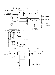
FIG. 2 depicts an exemplary implementation of fluorescent power supply (FPS)
100. As
shown, FPS 100 includes a battery charger 200, a double rate charger control
circuitry 205, a
controller 210, relay coils 215, a high frequency (HF) inverter/ballast AC
output
circuitry 220, an impedance network 225, and AC ballast control circuitry 230.
Battery
charging and light powering circuitry 140 of FIG. 1 may include components
200, 205, 210,
215, 220, 225 and 230 FPS 100 may additionally include rechargeable battery
130 and relay
contacts 150 that, as depicted in FIG. 1, may not be included in circuitry
140.
Battery charger 200 includes circuitry for supplying charging current to
battery 130. Double
rate charger control circuitry 205 controls an amount of charging current that
is supplied to
battery 130 via battery charger 200. In one implementation, circuitry 205 may
enable a high
rate of charging current or a low rate of charging current to be supplied to
battery 130 via
battery charger 200 for charging periods controlled by controller 210.
Controller 210 may include a processor, microprocessor, a microcontroller, or
processing
logic that performs processes, such as the exemplary process described below
with respect to
- 4 -
CA 02912240 2015-11-17
FIGs. 11-13. In implementations where controller 210 includes a processor,
microprocessor
or a microcontroller, controller 210 may interpret and execute instructions to
perform the
processes.
Relay coils 215 may, based on voltage and current supplied by battery charger
200, cause
relay contacts 130 to engage, connecting AC ballast 110 to power fluorescent
light 120 while
FPS 100 may charge battery 130. When battery charger 200 removes the voltage
and current
from relay coils 215 (e.g., due to AC input power failure), relay contacts 130
disengage,
connecting FPS 100 to power fluorescent light 120 instead of AC ballast 110.
HF
inverter/ballast AC output circuitry 220 includes circuitry for FPS 100 to
supply power to
fluorescent light 120 via impedance network 225. Impedance network 225
includes circuitry
for controlling the light output level of fluorescent light 120. AC ballast
control circuitry 230
includes circuitry for turning on or off external AC ballast 110.
FIG. 3 depicts details of the circuitry of an exemplary implementation of
battery charger 200.
As shown, AC input power (AC N, White, AC_H) is received as an input to bridge
rectifier D14 which converts the AC voltage to a DC voltage DC+. Charger
controller U4
receives the rectified AC input power as a DC input voltage (VDD) at pin 7 via
resistors R102, R103, R104, R101 and capacitors C32 and C103. In one
implementation,
charger controller U4 may include a FAN100 Pulse Width Modulated (PWM)
controller (Fairchild Semiconductor) that serves as a power supply constant-
voltage (CV)
and constant-current (CC) control unit for FPS 100.
Charger controller U4 controls the voltage and current supplied to relay coils
215 and
rechargeable battery 130 via isolating transformer T2. Pins 2 and 6 of charger
controller U4
are grounded. R51 and C28 connect to pin 3 and act to compensate current loop
gain. Pin 1
of charger controller U4 connects current sense resistor R49 to sense the
current through
MOSFET Q15 for peak-current-mode control in CV mode and output-current
regulation in
CC mode. R50 and C27 connect to pin 4 and act to compensate voltage loop gain.
Pin 5 of
charger controller U4 detects the output voltage and discharge time based on
the voltage
across the auxiliary winding of T2. Pin 5 also connects to divider resistors
R46 and R47 and
to capacitor C26. Pin 8 of charger controller U4 outputs the Pulse Width
Modulated (PWM)
- 5 -
CA 02912240 2015-11-17
signal to drive external MOSFET Q15. The output PWM signal from pin 8 of
charger
controller U4 turns on or off the supply of battery charging current through
resistors R53 and
R56 (FIG. 4). The output PWM control signal from pin 8 of charger controller
U4 has a
repetition rate that is sufficient to maintain, via transformer T2, a
relatively stable voltage and
current that charges capacitors C31A, C31B, C35 and C34 to, in turn, generate
voltage Vo+
that includes the charging voltage for supplying either a high charging rate
current or a low
charging rate current to rechargeable battery 130. The current through MOSFET
Q15, when
on, passes through the primary side of T2 to energize the transformer core.
Given the reverse
polarity of the windings (i.e., secondary relative to primary of T2) and with
D13 being
reverse biased, there is no energy transfer to the secondary of T2 when MOSFET
Q15 is on.
When MOSFET Q15 is turned off, the energy accumulated in the transformer core
is coupled
to the secondary of T2, forward biasing D13, and allowing current to flow
through, and
recharging, parallel capacitors C31A, C31B, C34 and C35 and generating voltage
Vo+ at the
connection (depicted with a "3" inside a rectangular box) from capacitors C35
and C34 to
one side of diode D6 and relay coils K3A, K4A, K5A, and K2A of relay coils 215
(see
FIG. 5). Voltage Vo+ actuates relay contacts 150, and enables power to be
supplied to
fluorescent light 120 from AC ballast 110. The amount of current supplied
through MOSFET
Q15 is controlled by double rate charger control circuitry 205, as described
further below.
Resistor R42, capacitor C24 and diode D10 act as a "snubber circuit", and are
active when
MOSFET Q15 is turned off to dissipate energy in the primary side of T2.
FIG. 4 depicts details of the circuitry of an exemplary implementation of
double rate charger
control circuitry 205. Double rate charger control circuitry 205 connects to
battery
charger 200 via the connection (depicted with a "1" inside a rectangular box)
at the drain of
MOSFET Q15 (see FIG. 3) that connects to resistors R53 and R56 (FIG. 4). The
current, for
charging battery 130, flows through R56 and/or R53. The values of R56 and R53
determine a
quantity of charging current supplied to battery 130. Resistor R53 sets a low
rate charging
current and resistor R56 sets a high rate charging current. The supply voltage
applied to pin 7
of charger controller U4 may also be applied via the connection (depicted with
a "2" inside a
rectangular box) to resistor R54 for supplying current through U5 and zener
diode DZ5.
Upon application of a control signal "stateCharger" from controller 210 (see
FIG. 9 below) to
resistor R55, the signal is coupled from resistor R55 to the gate of MOSET Q16
via
- 6 -
CA 02912240 2015-11-17
opto-coupler U5 to turn on or off MOSFET Q16. When Q16 is turned off, charging
current
only flows through resistor R53 (i.e., the low rate charging current). When
Q16 is turned on,
charging currently flows through resistors R56 and R53 (i.e., the high rate
charging current).
For example, when Q16 is turned off (i.e., a high control signal
"stateCharger"), a current of
approximately 220mA flows through resistor R53 and transistor Q15. As a
further example,
when Q16 is turned on (i.e., a low control signal "stateCharger"), a total
current of
approximately 265mA flows through resistors R53, R56 and transistor Q15.
Different
resistance values for R53 and R56 may be selected to change the two different
charging
current rates. A different resistance value for resistor R56 may be selected
to change the high
charging rate, and a different resistance value for resistor R53 may be
selected to change the
low charging rate.
FIG. 5 depicts details of an exemplary implementation of relay coils 215 as
connected to
rechargeable battery 130. Referring back to FIGs. 3 and 4, the current flow
through
MOSFET Q15 (FIG. 3) and resistor R53 and/or resistor R56 (FIG. 4) generates a
voltage on
the primary side of T2 (FIG. 3), which, when MOSFET Q15 is turned from on to
off based
on the PWM control signal from pin 8 of U4, is coupled across to the secondary
side of T2 to
power relay coils 215 as voltage Vo+ at the connection (depicted with a "3"
inside a
rectangular box) from capacitors C35 and C34 to one side of diode D6 and relay
coils K3A,
K4A, K5A, and K2A of relay coils 215 (FIG. 5). Voltage Vo+, and current
supplied by the
secondary side of T2, actuates relay contacts 150, enabling the supply of
power to fluorescent
light 120 via AC ballast 110. The amount of current supplied through MOSFET
Q15, and
therefore, the voltage level applied to the primary of T2, is controlled by
double rate charger
control circuitry 205, as described above with respect to FIG. 4. When the
voltage difference
between voltage Vo+ (at connection "3", FIG. 5) and Vbattõy is large enough,
the voltage drop
across relay coils K3A, K4A, K5A and K2A, and corresponding current flow
through the
relay coils, is sufficient to activate relay contacts 150 to enable AC ballast
110 to power
fluorescent light 120.
FIG. 6 depicts details of the circuitry of an exemplary implementation of
voltage regulation
circuitry 600, ballast AC output circuitry 610 and HF inverter circuitry 620
(of HF
inverter/ballast AC output circuitry 220) (depicted in FIG. 2), and impedance
network 225.
- 7 -
CA 02912240 2015-11-17
As shown in FIG. 6, voltage regulation circuitry 600 may receive voltage
Vbattery from
battery 130 via the connection depicted with a "4" inside a rectangular box.
Low voltage
linear regulator VR1 receives the voltage Vbattery via diode D8, and outputs a
regulated
voltage level Vcc for powering controller 210 via the connection identified by
a "10" within
a rectangular box. Low voltage linear regulator VR2 receives the voltage Vcc
from VR1, and
outputs a regulated reference voltage level Vref that is supplied to
controller 210 via a
connection identified by a "9" within a rectangular box. Controller 210 uses
the reference
voltage level Vref in its internal Analog-to-Digital converter.
Ballast AC output circuitry 610 may be turned on and off based on control
signal "DriverOn"
received from controller 210 via the connection identified by a "11" within a
rectangular box.
Ballast AC output circuitry 610 is turned on by a high "DriverOn" signal at
the gate of
MOSFET Q10, which drives MOSFET Q7. A high "DriverOn" signal at the gate of
MOSFET Q10 causes MOSFET Q7 to turn on which, in turn, causes current to flow
through Q7 and resistor R2 initiating the oscillation of transistors Q1 and Q2
of HF inverter
circuitry 620. A low "DriverOn" signal at the gate of MOSFET Q10 causes MOSFET
Q7 to
turn off which, in turn shuts off the flow of current through Q7 and R2,
stopping the
oscillation of transistors Q1 and Q2, thereby, stopping the operation of HF
inverter
circuitry 620.
HF inverter circuitry 620, when turned on by ballast AC output circuitry 610,
powers
fluorescent light 120 via impedance network 225 and relay contacts 150 using a
self
oscillating technique. Impedance network 225 includes capacitors Cl, C3, C5
and C50
whose values may be matched to the type of fluorescent light 120 connected to
impedance
network 225 via relay contacts 150. The light output of fluorescent light 120
may be adjusted
by modifying the capacitors in impedance network 225. Impedance network 225
may
connect, via connections identified by a "5", "6", "7", and "8" within
rectangular boxes, to
relay contacts 150 depicted in FIG. 7. The connections "VioletA" and "VioletB"
at each side
of capacitor Cl in impedance network 225 may be shorted together (e.g., via an
external wire
or jumper connected between "VioletA" and "VioletB") to augment power to
fluorescent
light 120 during, for example, emergency operation.
- 8 -
CA 02912240 2015-11-17
FIG. 7 depicts exemplary details of the interconnection of relay contacts 150
with external
AC ballast 110 and with FPS 100. As seen in FIG. 7, when the relay contacts
150 are in an
upper position (i.e., relay coils 215 unactivated), such as when the AC input
power has failed,
FPS 100 is connected to fluorescent light 120 so as to provide power to light
120. As
depicted in FIG. 6, the connections shown as 5, 6, 7 and 8 within rectangular
boxes connect
to impedance network 225 for receiving power from FPS 100 for powering
fluorescent
light 120, instead of AC ballast 110. When the relay contacts 150 are in a
lower position of
FIG. 7 (i.e., are activated by relay coils 215), such as when AC input power
is present, AC
ballast 110 is connected to fluorescent light 120 to provide power to light
120.
FIG. 8 depicts details of an exemplary implementation of AC ballast control
circuitry 230.
AC ballast control circuitry 230 turns on or off external AC ballast 110 for
supplying power
to fluorescent light 120 via relay contacts 150. Controller 210 may turn on or
off AC
ballast 110 via the External Ballast ON (EXB on) signal connection shown as a
"12" within
a rectangular box in FIG. 8. When control signal EXB_on is pulled low (logic
0), a current is
pulled from Vcc at the signal connection shown as a "10" within a rectangular
box in FIG. 8
through the photodiode of opto-coupler U3. The flow of current through the
photodiode of
opto-coupler U3 turns on the triac of opto-coupler U3 which, in turn, turns on
triac Q13.
When triac Q13 turns on, the voltage of the AC input power (AC_H at "black")
is connected
through triac Q13 to be supplied to AC ballast 110 (via "black/white"). When
control signal
EXB_on is pulled high (logic 1), the photodiode of opto-coupler U3 is placed
in an off
condition, thereby causing triac Q13 to be put in an off state. With triac Q13
in an off state,
AC input power (AC_H) at the "black" input connection is not supplied via
triac Q13 to
the "black/white" connection, thereby turning AC ballast 110 off.
In AC ballast control circuitry 230, the AC input power neutral connection
(AC_N) and the
high voltage of the AC input power (AC_H), in combination with resistors R6,
R23, R21,
R16, capacitor C9 and opto-coupler U2, provide an indication if fluorescent
light 120 is
turned on and the AC input power is being supplied (i.e., has not failed).
When the "black"
input is powered (i.e., AC input power is on), then current flows through U2
and R21 causing
the voltage level "Unoccupied" at the connection "13" within the rectangular
box of FIG. 8
to be pulled low. When fluorescent light 120 is turned off, or the AC input
power has failed,
- 9 -
CA 02912240 2015-11-17
then the voltage level "Unoccupied" at connection "13" is pulled high.
FIG. 9 depicts details of an exemplary implementation of controller 210 and
associated
circuitry. In the exemplary implementation of FIG. 9, controller 210 includes
a
programmable 8-bit PIC16F886 microcontroller from Microchip. Other types of
controllers,
however, may alternatively be used. The associated circuitry with controller
210 includes an
oscillator Y1 that sets controller 210's operating frequency via the OSC1 and
OSC2 pins.
Controller 210 is powered by voltage Vcc provided, from voltage regulation
circuitry 600 of
FIG. 6, via the connection identified by a "10" within a rectangular box.
Controller 210 may,
as depicted in FIG. 9, have various different input pins for receiving various
different input
signals and various different output pins for supplying output control signals
to other
circuitry within FPS 100. The use of the various output control signals from
controller 210
are described further with respect to the applicable portions of circuitry of
FPS 100 being
controlled. As described below with respect to FIGs. 11-13, controller 210 may
determine a
low voltage condition on battery 130, an AC input power failure, a forced
battery
discharge (e.g., due to testing of FPS 100), and/or a battery discharge time
during AC input
power failure. Controller 210 may control the operation of FPS 100 to select
one of multiple
different battery charging rates and to select one of multiple different
battery charging
periods based on a determined low voltage condition, an AC input power
failure, a forced
battery discharge, and/or battery discharge time.
FIG. 10 depicts an overview of the powering of fluorescent light 120 from AC
ballast 110 or
FPS 100 via relay contacts 150. As shown in FIG. 10, AC input power is applied
via
the "black" input to FPS 100. FPS 100, in turn, selectively supplies power to
AC ballast
via "white" and "blIc/wht" outputs. When the relay coils (not shown) are
unactivated (e.g.,
AC input power has failed) such that the contacts of relay contacts 150 are in
the right-wards
position shown in FIG. 10, the light powering circuitry of FPS 100 connects to
fluorescent
light 120 via "RedInt", "RedInt2", "YellowInt", and "YellowInt2" to supply
power to
light 120 via "Red", "Red/wht", "Yellow", "Yellow/wht", and "Yellow". When
relay
contacts 150 are activated (e.g., AC input power is present) such that the
contacts are in a
left-wards position (not shown in FIG. 10), AC ballast 110 supplies power to
light 120
via "Blue/Wht", "Blue", "Brown/Wht", and "Brown" from AC ballast 110 and via
"Red",
- 10-
CA 02912240 2015-11-17
"Red/wht", "Yellow", and "Yellow/wht", to fluorescent light 120.
FIGs. 11-13 are flow diagrams that illustrate an exemplary process for
charging rechargeable
battery 130 of emergency lighting fluorescent power supply 100 using a
selected one of at
least two different charging rates for selected charging periods. The
exemplary process of
FIGs. 11-13 may be performed by controller 210 in conjunction with other
components of
FPS 100, or external AC ballast 110.
The exemplary process may include controller 210 determining if a low battery
voltage has
been detected at rechargeable battery 130 (block 1105). Controller 210 may
monitor a
voltage (Vbat - at resistor R38, FIG. 9) indicative of the current battery
voltage level. The
voltage (Vbat) is proportional to the actual battery voltage (Bat+ - FIGs. 5
and 9). If
controller 210 determines that a low battery voltage has been detected at
battery 130 (YES -
block 1105), then controller 210 causes battery 130 to be charged using a high
charging rate
for a maximum recharge time (block 1110). In one implementation, the maximum
recharge
time has been specified as 26 hours. Other maximum recharge times may,
however, be
specified. To charge battery 130 at the high charging rate, controller 210
applies a
low "stateCharger" signal at resistor R55 of double rate charger control
circuitry 205 (see
FIG. 4). Upon application of the low "stateCharger" signal from controller 210
(see FIG. 9),
the signal is coupled from resistor R55 to the gate of MOSET Q16 via opto-
coupler U5 to
turn on MOSFET Q16. When Q16 is turned on, charging currently flows through
both
resistors R56 and R53. As an example, when Q16 is turned on (i.e., a low
control
signal "stateCharger"), a current of approximately 265mA flows through
resistors R53, R56
and transistor Q15 (see FIG. 3). The current flowing through transistor Q15 is
coupled, when
Q15 is turned from on to off based on the PWM control signal from U4, via
transformer T2
to supply a charging voltage Vo+, via capacitors C31A, C31B, C35 and C34, at
one side of
relay coils K2A, K3A, K4A, and K5A (see FIG. 5), with a corresponding charging
current
that flows through relay coils K2A, K3A, K4A, and K5A into battery 130. Upon
application
of the low "stateCharger" signal, controller 210 may initiate an internal
timer to time the
interval for the maximum recharge time. Upon expiration of the maximum
recharge time, as
indicated by the internal timer, controller 210 may cause the supply of
charging current to
battery 130 to be reduced to a low charging rate. To reduce the charging
current to a low
- 11 -
CA 02912240 2015-11-17
charging rate, controller 210 applies a high "stateCharger" signal at resistor
R55 of double
rate charger control circuitry 205 (see FIG. 4). Upon application of the high
"stateCharger"
signal from controller 210 (see FIG. 9), the signal is coupled from resistor
R55 to the gate of
MOSET Q16 via opto-coupler U5 to turn off MOSFET Q16. When Q16 is turned off,
charging current flows through resistor R53, and not through resistor R56.
Controller 210 may monitor the charging current flowing into battery 130 by
first measuring
current values for a voltage (Vcharge - at resistor R40, FIG. 9) indicative of
the voltage Vo+
applied at the one side of relay coils K2A, K3A, K4A, and K5A and the voltage
(Vbat - at
resistor R38, FIG. 9) indicative of the current battery voltage level. The
voltage (Vbat) is
proportional to the battery voltage (Bat+ - FIGs. 5 and 9) and the voltage
Vcharge is
proportional to voltage Vo+. Controller 210 may calculate the charging current
by
determining the difference between the Vo+ and Bat+ voltages and dividing the
difference
value by a fixed resistance value from the known impedance of the parallel
connected
relays K2A, K3A, K4A, and K5A.
Referring back to FIG. 11, if controller 210 does not detect a low battery
voltage at
battery 130 (NO - block 1105), then the exemplary process continues at
block 1200 (FIG. 12), with controller 210 determining if an AC input power
failure has
occurred. Controller 210 may monitor the AC input power voltage level to
identify whether a
sufficient voltage level exists. If an AC input power failure has occurred
(YES - block 1200),
then controller 210 determines a length of time that battery 130 has
discharged (i.e., the
discharge time or discharge period), between the instant the AC input power
failed and until
the AC input power resumed, to power fluorescent light 120 (block 1205).
Controller 210
may initiate an internal timer at the instant an insufficient voltage level at
the AC input power
is determined to exist. The internal timer may continue to count until a
sufficient voltage
level at the AC input power is detected again. The value for the internal
timer (in
minutes/seconds) at the instant that a sufficient voltage level is detected at
the AC input
power is the battery discharge time.
Controller 210 determines if the discharge time is greater than or equal to a
threshold number
of minutes (block 1210). In one implementation, the threshold number of
minutes may be
- 12 -
CA 02912240 2015-11-17
sixty minutes. In other implementations, different lengths of a threshold time
may be
alternatively used. If the discharge time is less than the threshold number of
minutes (NO -
block 1210), then controller 210 sets a high rate charging time (CT) equal to
the determined
discharge time multiplied by a fixed factor (block 1215). In one
implementation, the fixed
factor may be a constant value, such as, for example, a constant value of 16.
Controller 210
may cause battery 130 to be charged using a high charging rate for the high
rate charging
time (CT), but not longer than the specified maximum recharge time (see block
1110
above) (block 1220). Controller 210 may cause battery 130 to be charged using
the high
charging rate for at least a minute regardless of the high rate charging time
(CT) that happens
to be set to ensure that sufficient current is initially available to cause
relays
coils K2A, K3A, K4A and K5A to activate the corresponding relay contacts 150.
To charge battery 130 at the high charging rate, controller 210 applies a low
"stateCharger"
signal at resistor R55 of double rate charger control circuitry 205. Upon
application of the
low "stateCharger" signal (see FIG. 9), the signal is coupled from resistor
R55 to the gate of
MOSET Q16 via opto-coupler U5 to turn on MOSFET Q16. When Q16 is turned on,
charging currently flows through both resistors R56 and R53. As an example,
when Q16 is
turned on (i.e., a low control signal "stateCharger"), a current of
approximately 265mA flows
through resistors R53, R56 and transistor Q15. The current flowing through
transistor Q15 is
coupled, when Q15 is turned from on to off via the PWM control signal from U4,
via
transformer T2 to supply a charging voltage Vo+ at one side of relay coils
K2A, K3A, K4A,
and K5A (FIG. 5), with a corresponding charging current that flows through
relay
coils K2A, K3A, K4A, and K5A into battery 130. Upon application of the
low "stateCharger" signal, controller 210 may initiate an internal timer to
time the interval
for the high rate charging time (CT).
Subsequent to the high rate charging of battery 130 during the high rate
charging time,
controller 210 may cause battery 130 to be charged using low rate charging
(block 1225).
Upon expiration of the high rate charging time (CT), as indicated by the
internal timer,
controller 210 may apply a high "stateCharger" signal to resistor R55 (see
FIG. 9) and the
signal is coupled from resistor R55 to the gate of MOSET Q16 via opto-coupler
U5 to turn
off MOSFET Q16. When Q16 is turned off, the current flowing through resistor
R56 ceases
- 13 -
CA 02912240 2015-11-17
to flow such that only charging current through R53 continues to flow. As an
example,
when Q16 is turned off (i.e., a high control signal "stateCharger"), a current
of
approximately 220mA flows through resistor R53 and transistor Q15. The current
flowing
through transistor Q15 is coupled, when Q15 is turned from on to off based on
the PWM
control signal from U4, via transformer T2 to supply a charging voltage Vo+ at
one side of
relay coils K2A, K3A, K4A, and K5A (FIG. 5), with a corresponding charging
current that
flows through relay coils K2A, K3A, K4A, and K5A into battery 130. The
exemplary
process may continue at block 1300 (FIG. 13).
Returning to block 1210, if controller 210 determines that the discharge time
is greater than
or equal to the threshold number of minutes (YES - block 1210), then
controller 210 causes
battery 130 to be charged using the high rate charging for the maximum
recharge
time (block 1230). Similar to block 1110 above, to charge battery 130 at the
high charging
rate, controller 210 applies a low "stateCharger" signal at resistor R55 of
double rate charger
control circuitry 205. Upon application of the low "stateCharger" signal (see
FIG. 9), the
signal is coupled from resistor R55 to the gate of MOSET Q16 via opto-coupler
U5 to turn
on MOSFET Q16. When Q16 is turned on, charging currently flows through both
resistors R56 and R53. As an example, when Q16 is turned on (i.e., a low
control
signal "stateCharger"), a current of approximately 265mA flows through
resistors R53, R56
and transistor Q15. The current flowing through transistor Q15 is coupled,
when Q15 is
turned from on to off based on the PWM control signal from U4, via transformer
T2 to
supply a charging voltage Vo+ at one side of relay coils K2A, K3A, K4A, and
K5A (FIG. 5),
with a corresponding charging current that flows through relay coils K2A, K3A,
K4A,
and K5A into battery 130. Upon application of the low "stateCharger" signal,
controller 210
may initiate an internal timer to time the interval for the maximum recharge
time (e.g., 26
hours). Upon expiration of the maximum recharge time, as indicated by the
internal timer,
controller 210 may cause the supply of charging current to battery 130 to be
reduced to the
low charging rate (block 1225 - as described above). The exemplary process
then continues
at block 1300 (FIG. 13).
Referring to FIG. 13, at block 1300, controller 210 determines if battery 130
has undergone a
forced discharge. Controller 210 may test FPS 100 by initiating a testing of
battery 130
- 14 -
CA 02912240 2015-11-17
discharging and charging. If controller 210 determines that battery 130 has
not undergone a
forced discharge (NO - block 1300), then the process may return to block 1100
(FIG. 11) to
loop through the process of FIGs. 11-13 again. If battery 130 has undergone a
forced
discharge (YES - block 1300), then controller 210 determines a length of time
that
battery 130 discharged (i.e., the discharge time) (block 1305). Block 1305 is
performed
similarly to block 1205 as described above.
Controller 210 determines if the discharge time is greater than or equal to a
threshold number
of minutes (block 1310). In one implementation, the threshold number of
minutes may be
sixty minutes. In other implementations, different lengths of discharge time
may be
alternatively used. If the discharge time is less than the threshold number of
minutes (NO -
block 1310), then controller 210 sets a high rate charging time (CT) equal to
the determined
discharge time multiplied by a fixed factor (block 1315). In one
implementation, the fixed
factor may be a constant value, such as, for example, a constant value of 16.
Block 1315 may
be performed similarly to block 1215 described above. Controller 210 may cause
battery 130
to be charged using a high charging rate for the high rate charging time (CT),
but not longer
than the specified maximum recharge time (see block 1110 above) (block 1320).
Controller 210 may cause battery 130 to be charged using the high charging
rate for at least a
minute regardless of the high rate charging time (CT) that happens to be set.
Block 1320 may
be performed similarly to block 1220 described above.
Subsequent to the high rate charging of battery 130 during the high rate
charging time,
controller 210 may cause battery 130 to be charged using low rate charging
(block 1325).
Block 1325 may be performed similarly to block 1225 described above. The
exemplary
process may return to block 1100 (FIG. 11) to loop again through the process
depicted in
FIGs. 11-13.
Returning to block 1310, if controller 210 determines that the discharge time
is greater than
or equal to the threshold number of minutes (YES - block 1310), then
controller 210 causes
battery 130 to be charged using the high rate charging for the maximum
recharge
time (block 1330). Block 1330 may be performed similarly to block 1230
described above.
Upon expiration of the maximum recharge time, as indicated by the internal
timer,
- 15 -
. CA 02912240 2015-11-17
controller 210 may cause the supply of charging current to battery 130 to be
reduced to the
low charging rate (block 1325 - as described above) The exemplary process may
then return
to block 1100 (FIG. 11) to loop again through the process depicted in FIGs. 11-
13.
The foregoing description of implementations provides illustration and
description, but is not
intended to be exhaustive or to limit the invention to the precise form
disclosed.
Modifications and variations are possible in light of the above teachings or
may be acquired
from practice of the invention. For example, while a series of blocks has been
described with
respect to FIGs. 11, 12 and 13 the order of the blocks may be varied in other
implementations. Moreover, non-dependent blocks may be performed in parallel.
Certain features described above may be implemented as "logic" or a "unit"
that performs
one or more functions. This logic or unit may include hardware, such as one or
more
processors, microprocessors, application specific integrated circuits, or
field programmable
gate arrays, software, or a combination of hardware and software.
Although the invention has been described in detail above, it is expressly
understood that it
will be apparent to persons skilled in the relevant art that the invention may
be modified
without departing from the spirit of the invention. Various changes of form,
design, or
arrangement may be made to the invention without departing from the spirit and
scope of the
invention. Therefore, the above-mentioned description is to be considered
exemplary, rather
than limiting, and the true scope of the invention is that defined in the
following claims. For
example, the configuration of components depicted in FIGs. 1-10 is for
illustrative purposes.
Other circuitry configurations may be implemented. Therefore, the circuitry
depicted in
FIGs. 1-10 may include additional, fewer and/or different components that may
be
configured in a different arrangement than those arrangements depicted.
No element, act, or instruction used in the description of the present
application should be
construed as critical or essential to the invention unless explicitly
described as such. Also, as
used herein, the article "a" is intended to include one or more items.
Further, the phrase
"based on" is intended to mean "based, at least in part, on" unless explicitly
stated otherwise.
- 16 -