Note: Descriptions are shown in the official language in which they were submitted.
CA 02914226 2015-12-01
WO 2014/196646 1
PCT/JP2014/065164
[Description]
[Title of Invention] NON-CONTACT COMMUNICATION METHOD DETERMINATION
CIRCUIT, NON-CONTACT COMMUNICATION CIRCUIT, AND IC CARD
[Technical Field]
[0001]
The present invention relates to a non-contact communication method
determination
circuit which determines whether or not a binary signal of a received radio
signal is a binary
signal of a radio signal with any of a plurality of non-contact communication
methods, a
non-contact communication circuit, and an IC card.
[Background Art]
[0002]
Recently, the use of non-contact IC cards has become widespread in the fields
of
electronic money, an electronic tickets or the like. A near-field wireless
communication
method and a non-contact communication protocol such as Type-A (Type A,
registered
trademark), Type-B, or Felica, (registered trademark) have been defined
International
Standards such as ISO / IEC 14443 or ISO / IEC 18092. According to the ISO /
IEC 18092, -
NFCIP-1 (Near-Field Communication Interface and Protocol) is defined while
including
Felica and Type-A of ISO / IEC 14443. According to ISO / IEC 21481 (NFCIP-2),
IS015693 (non-contact vicinity IC card) and Type-B of ISO / IEC 14443 are
defined in
addition to NFCIP-1.
[0003]
It is necessary to determine which of a plurality of communication methods
should be
applied for sending a frame, such that an IC card or a reader-writer
corresponding to a
plurality of communication methods decodes data in the communication frame.
[0004]
For example, Patent Document 1 (JP 2002-342725A) discloses a configuration
which
2
measures a pulse width of a binary signal, compares the pulse width with a
pulse width
defined by each communication method, and selects an identical pulse width, so
as to
determine a communication method. For example, Patent Document 2 (JP 2010-
183423A)
discloses a configuration of pattern matching which samples a binary signal
with a
predetermined clock for a predetermined time, compares the data pattern of the
sampling
result with a previously held data pattern of each communication method, and
selects an
identical data pattern.
[0005]
However, because an analogue circuit is generally used for a demodulator, a
binary
signal as a demodulation result includes pulse variations due to code
interference,
distortion, or the like by the analogue circuit. For this reason, it becomes
difficult to
determine a communication method based on the measurement of the pulse width
or the
pattern matching, resulting in a communication method determination error.
[Summary of Invention]
[0006]
An object of the present invention is to solve the above problem, and to
provide a
non-contact communication method determination circuit which can prevent a
communication method determination error.
[0007]
According to one embodiment, there is provided a non-contact communication
method determination circuit for determining whether or not a binary signal of
a received
radio signal is a binary signal of a radio signal conforming to any of a
plurality of first non-
CA 2914226 2017-11-06
3
contact communication methods, the circuit comprising: a demodulator
configured to
demodulate the received radio signal into a binary signal and including a
clock regenerator
which regenerates a clock having a frequency fc based on the received signal;
an edge
detector configured to detect a rising edge of the binary signal and generate
a reset signal; a
counter configured to count pulses of the clock from the clock regenerator and
to reset a
counter value to 0 in response to the reset signal; and a determiner
configured to compare
the counter value with a predetermined value, so as to determine whether or
not the binary
signal of the received radio signal is a binary signal of a radio signal
conforming to any of
the plurality of first non-contact communication methods.
[0007a]
According to another embodiment, there is provided a non-contact communication
circuit, comprising: a decoder which decodes the demodulated binary signal
into data; an
encoder which encodes the data input from the decoder into a binary signal; a
modulator
which modulates a carrier wave into a radio signal in accordance with the
encoded binary
signal; and the non-contact communication method determination circuit
described herein,
wherein the decoder is configured to decode the demodulated binary signal into
data, and
outputs the data with a first non-contact communication method determined by
the non-
contact communication method determination circuit, and the encoder is
configured to
encode the data input from the decoder into a binary signal with the first non-
contact
communication method, and the modulator is configured to modulate a carrier
wave into a
radio signal in accordance with the encoded binary signal with the first non-
contact
communication method.
CA 2914226 2017-11-06
3a
[0007b1
According to another embodiment, there is provided a non-contact communication
circuit, comprising: the non-contact communication method determination
circuit
described herein; a first demodulator which demodulates a received radio
signal into a
binary signal; a first decoder which decodes the binary signal demodulated by
the first
demodulator into data with a first non-contact communication circuit
determined by the
non-contact communication method determination method; a first encoder which
encodes
the data decoded by the first decoder into a binary signal with a second non-
contact
communication method different from the determined first non-contact
communication
method; a first modulator which modulates the binary signal encoded by the
first encoder
into a modulated signal, and outputs the modulated signal with the second non-
contact
communication method; a second demodulator which demodulates the modulated
signal
input from the first modulator into a binary signal with the second non-
contact
communication method; a second decoder which decodes the binary signal
demodulated
by the second demodulator into data with the second non-contact communication
method;
a second encoder which encodes the data decoded by the second decoder into a
binary
signal with the determined first non-contact communication method; and a
second
modulator which modulates a carrier wave into a radio signal in accordance
with the binary
signal encoded by the second encoder with the determined first non-contact
communication method.
CA 2914226 2017-11-06
3b
[0007c]
According to another embodiment, there is provided a non-contact communication
circuit, comprising: the non-contact communication method determination
circuit
described herein; a first decoder which decodes the binary signal demodulated
by the
demodulator into data with a first non-contact communication method determined
by the
non-contact communication method determination circuit; a first encoder which
encodes
the data decoded by the first decoder into a binary signal, and outputs the
binary signal
with a second non-contact communication method different from the determined
first non-
contact communication method; a second decoder which decodes the binary signal
input
from the first encoder into data with the second non-contact communication
method;
a second encoder which encodes the data decoded by the second decoder into a
binary
signal with the determined first non-contact communication method; and a
modulator
which modulates a carrier wave into a radio signal in accordance with the
binary signal
encoded by the second encoder with the determined first non-contact
communication
method.
[Brief Description of Drawings]
[0008]
FIG. 1 is a general side view illustrating a configuration of an IC card
system
according to Embodiment 1 of the present invention.
FIG. 2 is a block diagram illustrating a configuration of an IC card 1
illustrated in
FIG. I.
CA 2914226 2017-11-06
3c
FIG. 3 is a block diagram illustrating a configuration of a decoder 22
illustrated in
FIG. 2.
FIG. 4 is a block diagram illustrating a configuration of a system determiner
illustrated in FIG. 3.
FIGS. 5A to 5D are timing charts illustrating a relationship between a binary
signal
and transmitted data of an encoding method for use in data transmission of
communication
methods of Type-A, Type-B, and Felica from a reader-writer 2 to the IC card 1
illustrated
in FIG. I.
FIGS. 6A to 6C are timing charts illustrating a frame configuration for use in
data
transmission of communication systems of Type-A, Type-B, and Felica from the
reader-
writer 2 to the IC card 1 illustrated in FIG. 1.
FIGS. 7A to 7C are flow charts illustrating a communication method
determination
process which is executed by the method determiner 32 illustrated in FIG. 4;
FIG. 7A
illustrates a first part of the process, FIG. 7B illustrates a second part of
the process, and
FIG. 7C illustrates a third part of the process.
FIG. g is a timing chart illustrating a setting example of a tolerable jitter
of a
counter
CA 2914226 2017-11-06
CA 02914226 2015-12-01
WO 2014/196646 4
PCT/JP2014/065164
value Dc, which tolerable jitter of a timing of falling of a binary signal,
and determines the
counter value Dc in the communication method determination process in FIGS. 7A
to 7C.
FIG 9A is a block diagram illustrating the configuration of an IC card 1A
according
to Embodiment 2 of the present invention.
FIG. 9B is a block diagram illustrating the configuration of a binary signal
processor
22A illustrated in FIG. 9A.
FIG 9C is a block diagram illustrating the configuration of a modulation
signal
processor 27A illustrated in FIG. 9A.
FIG. 10A is a block diagram illustrating the configuration of an IC card 1B
according
to Embodiment 3 of the present invention.
FIG 10B is a block diagram illustrating the configuration of a binary signal
processor
22B illustrated in FIG. 10A.
FIG 10C is a block diagram illustrating the configuration of a binary signal
processor
27B illustrated in FIG. 10A.
[Description of Embodiments]
[0009]
Hereinafter, embodiments of the present invention will be described with
reference to
the drawings. In addition, the same reference numbers are applied to similar
elements in
each embodiment.
[0010]
Embodiment 1
FIG. 1 is a general side view illustrating the configuration of an IC card
system
according to Embodiment 1. In FIG 1, a non-contact communication circuit 20 of
the IC
card 1 for use in the IC card system of the present embodiment receives a
radio signal of a
modulated signal. The non-contact communication circuit 20 demodulates the
received radio
signal into a binary signal, determines which of the binary signals of the
radio signals of a
CA 02914226 2015-12-01
WO 2014/196646 5
PCT/JP2014/065164
plurality of non-contact communication methods (hereinafter, referred to as
communication
method) illustrated in Table 1, for example, is the binary signal of the
received radio signal
based on a time interval between falling edges of the demodulated binary
signal, and
determines which communication method and transmission rate of a plurality of
communication methods should be applied for the wireless communication from
the
reader-writer 2.
[0011]
In FIG. 1, the reader-writer 2 is provided in an electronic device 3 which
identifies
and authorizes a user of the IC card 1, and provides a service for a user, for
example. The
electronic device 3 is, for example, an automatic ticket gate, automatic money
machine, or
attendance and leaving management device. The reader-writer 2 encodes digital
transmitted
data by a predetermined communication method using a non-contact
communication,
generates a binary signal, modulates a carrier wave in accordance with the
binary signal, and
outputs the modulated carrier wave as a radio signal.
[0012]
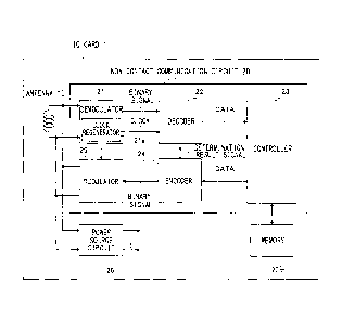
FIG. 2 is a block diagram illustrating the configuration of the IC card 1
illustrated in
FIG 1. Referring to FIG 2, the IC card 1 includes an antenna 10, the non-
contact
communication circuit 20 made of a semiconductor integrated circuit such as an
LSI, and a
power source circuit 26. The non-contact communication circuit 20 includes a
demodulator
21, a decoder 22, a controller 23, a memory 23m connected to the controller
23, an encoder 24,
and a modulator 25. In FIG 2, the distance between the IC card 1 and the
reader-writer 2 is a
short distance, for example, 1 to 30 cm, the antenna 10 receives the radio
signal from the
reader-writer 2, and outputs the radio signal to the power source circuit 26
and the
demodulator 21 as a received signal. The power source circuit 26 receives the
received
signal as an AC voltage signal, and rectifies it to DC voltage, so as to
supply the DC voltage to
each section 21, 22, 23, 24, 25, 23m constituting the non-contact
communication circuit 20.
CA 02914226 2015-12-01
WO 2014/196646 6
PCT/JP2014/065164
In this case, the demodulator 21 demodulates the received signal into a binary
signal, and
outputs the binary signal to the decoder 22. The demodulator. 21 includes a
clock regenerator
21a which regenerates a clock having a frequency fc based on the received
signal having a
carrier wave of a frequency fc of 13.56 MHz, for example, and outputs the
clock to the
decoder 22. One clock is 1 / fc.
[0013]
The decoder 22 decodes the binary signal from the demodulator 21 using a
communication method used in the reader-writer 2, generates logical data, and
outputs the data
to the controller 23. The decoder 22 determines the communication method by
using the
clock from the clock regenerator 21a based on the binary signal from the
demodulator 21, and
decodes the binary signal from the demodulator 21 into data with an encoding
method defined
in the determined communication method. The decoder 22 outputs a determination
result
signal showing the determination result to the encoder 24 and the modulator
25.
[0014]
The controller 23 executes a predetermined process based on a program stored
in the
memory 23m connected to the controller 23 and the data from the decoder 22,
generates data
to be transmitted to the reader-writer 2, and outputs the data to the encoder
24. The
above-described predetermined process includes a process of generating data
which should be
transmitted, for example, an ID or other data of the IC card 1. The encoder 24
encodes the
data received from the controller 23 into a binary signal, and outputs the
signal to the
modulator 25 using the communication method used in the reader-writer 2 in
accordance with
the determination result signal from the decoder 22. The modulator 25
modulates the carrier
wave into a modulated signal in accordance with the binary signal from the
encoder 24, and
transmits the signal to the reader-writer 2 through the antenna 10 using a
communication
method shown in the determination result signal.
[0015]
CA 02914226 2015-12-01
WO 2014/196646 7
PCT/JP2014/065164
FIG 3 is a block diagram illustrating the configuration of the decoder 22
illustrated in
FIG 2. Referring to FIG. 3, the decoder 22 includes a decoding section 31, and
a method
determiner 32 to which a clock is supplied from the clock regenerator 21a. The
system
determiner 32 determines which communication method (modulation method,
encoding
method, data transmission rate) is used for encoding the binary signal in the
reader-writer 2 by
using the clock based on the binary signal from the demodulator 21. The method
determiner
32 outputs the determination result signal illustrating the determination
result to the decoding
section 31, encoder 24 and modulator 25. In addition, the system determiner 32
executes the
communication method determination process by reading a program of the
communication
method determination process for determining a communication method and a
transmission
rate, and data required for executing the program, which are stored in a
memory circuit such as
a memory 32m in the method determiner 32. The details of the communication
method
determination process will be described with reference to FIGS. 7A to 7C. The
decoding
section 31 decodes the binary signal from the demodulator 21 into data, and
outputs the data to
the controller 23 using the communication method shown by the determination
result signal
from the method determiner 32.
[0016]
FIG 4 is a block diagram illustrating the configuration of the system
determiner 32
illustrated in FIG 3. In FIG 4, the system determiner 32 includes a falling
edge detector 41,
a counter 42, and a method and transmission rate determiner 43. The method
determiner 32
in FIG 4 constitutes a non-contact communication method determination circuit,
and may
= include the clock regenerator 21a.
[0017]
In FIG. 4, the falling edge detector 41 detects the falling of the binary
signal from the
demodulator 21, outputs a reset signal indicating the detection of the falling
of the binary
signal to the counter 42, and resets the calculation value of the counter 42
to 0. The falling
CA 02914226 2015-12-01
WO 2014/196646 8
PCT/JP2014/065164
edge detector 41 outputs the detection signal to the method and transmission
rate determiner
43 when detecting the falling of the binary signal. In this case, the counter
42 calculates the
pulse of the clock from the clock regenerator 21a, and outputs the data of
counter value Dc to
the method and transmission rate determiner 43. In addition, a clock can be
supplied to the
counter 42 from an external circuit.
[0018]
The method and transmission rate determiner 43 determines which communication
method and transmission rate of a plurality of communication methods should be
applied for
encoding the binary signal with the reader-writer 2 based on the detection
signal from the
falling edge detector 41 and the data of the counter value De from the counter
42. The
method and transmission rate determiner 43 outputs the determination result
signal indicating
the determination result to the decoding section 31.
In this case, a plurality of
communication methods includes, for example, Type-A, Type-B, and Felica. Table
1
illustrates the specifications of the communication methods, Type-A, Type-B,
and Felica.
[0019]
[Table 1]
CA 02914226 2015-12-01
WO 2014/196646 9
PCT/JP2014/065164
TRANSM I SS I ON
DIRECTION ITEM Type¨A Type¨B
Felica
OPERATION 13.56 13.56 13.56
FREQUENCY " : 7kHz 7kHz .-7kHz
MODULATION
METHOD ASK ASK ASK
MODULATION
DEGREE 100% 8 to 14% 8 to 30%
READER-WRITER
ENCODING MODIFIED MIRROR NRZ
MANCHESTER
NON-CONTACT
IC CARD
TRANSMISSION 106,212, 106,212, 212,
RATE 424,828kbps 424,828kbps 424,kbps
SUBCARR I ER
FREQUENCY 847.5kHz 847.5kHz 847.5kHz
COMMUNICATION
NON-CONTACT METHOD LOAD SWITCH LOAD SWITCH
LOAD SWITCH
IC CARD
MODULATION OOK
READER-WRITER METHOD OR BPSK OOK
BPSK
MANCHESTER
ENCODING OR NRZ L MANCHESTER
NRZ_L
TRANSMISSION 106,212, 106,212, 212,
RATE 424,828kbps 424,828kbps 424,kbps
[0020]
Table 1 shows a transmission direction for each communication method, and a
modulation method, modulation degree, encoding method, and transmission rate
for each
communication method. As shown in Table 1, in the specification of each
transmission
method, for example, the encoding method, modulation method, and transmission
rate differ
according to a transmission direction of a signal from the reader-writer 2 to
the IC card 1 or
from the IC card 1 to the reader-writer 2.
[0021]
FIGS. 5A to 5D are timing charts illustrating a relationship between the
binary signal
CA 02914226 2015-12-01
WO 2014/196646 10
PCT/JP2014/065164
and transmitted data of the encoding method for use in the data transmission
with the
communication methods of Type-A, Type-B, and Felica from the reader-writer 2
to the IC card
1 in FIG 1.
[0022]
In the case of the communication method of Type-A in which the transmission
rate is
106 kbps (hereinafter referred to as communication method of Type-A and 106
kbps)
illustrated in FIG. 5A, the transmitted data is ASK (Amplitude Shift Keying)
modulated by a
modulated mirror, and the data of the logical values "1" and "0" is
represented based on the
position of the signal (hereinafter referred to as pause pulse) in which a
magnetic field output
in a bit data interval is stopped. In the modulated signal, the bit data
having the pause pulse
in the center of the bit data shows the logical value "1". The bit data having
the pause pulse
in the head portion of the bit data and the bit data without having the pause
pulse in the head
portion of the bit data show the logical value "0". Regarding the
communication method and
the transmission rate, the time interval between the falling edges formed in
the waveform of
the binary signal (hereinafter referred to as falling edge interval) is 128 /
fc or 192 / fc. A
start bit S having the logical value "0" of one bit is provided in the head of
the communication
frame.
[0023]
In the case of the communication method of Type-A and 212 kbps illustrated in
FIG
5B, the transmission rate of the binary signal is twice that shown in FIG 5A.
Thus, the
binary signal includes the falling edge interval of 64 / fc and 96 / fc.
[0024]
In the case of the communication method of Type-B and 106 kbps illustrated in
FIG
5C, when the transmitted data is transmitted from the reader-writer 2 to the
IC card 1, the
transmitted data is encoded into the binary signal by an NRZ (Non-Return to
Zero) code.
The binary signal is further ASK-modulated, so that the logical values "1" and
"0" are
CA 02914226 2015-12-01
WO 2014/196646 11
PCT/JP2014/065164
indicated. A signal having a large amplitude of a carrier wave, which is not
modulated,
indicates the logical value "1", and a signal having a small amplitude of a
carrier wave
indicates the logical value "0". Regarding the communication method and the
transmission
rate, the falling edge interval of the binary signal is, for example, 128 /
fc. In addition, the
head of the data portion of the communication frame includes one bit (data
value 0) as a start
bit.
[0025]
In the case of the communication method of Felica and 212 kbps illustrated in
FIG.
5D, the transmitted data is encoded into a binary signal by a Manchester
encoding method.
The binary signal is farther ASK-modulated, so that the data of the logical
values "1" and "0"
is indicated. The signal having large amplitude of a carrier wave in the first
half of the bit
data interval and having small amplitude of a carrier wave in the second half
of the bit data
interval indicates the logical value "1". With this communication method and
the
transmission rate, a polarity can be distinguished when receiving a specific
code in a frame
even if a polarity is reversed. A preamble made of the logical value "0"
having a length of 48
bits is provided in the head of the communication frame with the present
communication
method.
[0026]
As described with reference to FIGS. 5A-5D, the falling edge interval of the
binary
signal differs with respect to each communication method and transmission rate
of a signal.
[0027]
Table 2 shows a counter value Dc of a standard falling edge interval of each
transmission rate of encoding in each communication method of Type-A and
Felica, and a
counter value Dc from the head of the frame to the next falling edge of each
transmission rate
of encoding in the communication method of Type-B.
[0028]
CA 02914226 2015-12-01
WO 2014/196646 12
PCT/JP2014/065164
[Table 2]
106kbps 212kbps 424kbps 848kbps
Type-A 128 or 192 64 or 96 32 or 48 16 or 24
1536 768 384 192
Type-B to 1792 to 896 to 448 to 224
Felica 64 32
[0029]
According to Table 2, the transmission rate of each communication method of
Type-A
and Type-B includes 106 kbps, 212 kbps, 424 kpbs, and 848 kbps. The
transmission rate of
the communication method of Felica includes 212 kbps and 424 kbps. The data in
Table 2 is
stored in the memory 32m, and the method determiner 32 specifies the
communication method
and transmission rate with reference to the data when executing the
communication method
determination process.
[0030]
FIGA. 6A to 6C are timing charts showing a frame configuration for use in the
data
transmission using the communication method of Type-A, Type-B, and Felica from
the
read-writer 2 to the IC card 1 in FIG 1.
[0031]
The communication frame of Type-A illustrated in FIG 6A includes a short frame
for
use in the beginning of the communication, a standard frame for use in a
normal command,
and a collision-prevention frame for use in a collision-prevention command.
Table 3 shows
bit data b0 to b6 in the short frame illustrated in FIG. 6A with respect to
each command.
[0032]
[Table 3]
CA 02914226 2015-12-01
WO 2014/196646 13
PCT/JP2014/065164
b6 b5 b4 b3 b2 b1 b0
0 1 0 0 1 1 0 REQA
1 0 1 0 0 1 0 WUPA
o 1 1 0 1 0 1 TIME SLOT
1 0 0 X X X X
1 1 1 1 X X X
[0033]
The short frame illustrated in FIG 6A includes a start bit S having a logical
value "0",
bit data made of bit data b0 to b6 in Table 3, and an end bit E. In the short
frame, any of the
bit data b0 to b6 is "1". The standard frame includes a start bit S having a
logical value "0",
1 byte data, a parity bit P. and an end bit E. In this case, the 1 byte data
and the parity bit P
are provided to be alternately located between the start bit S and the end bit
E. In FIG. 6A, S
denotes a start bit, E denotes an end bit, and P denotes a parity bit. The
parity bit is an odd
parity. When the number of logical values "1" in the 1 byte data is an odd
number, the
logical value is "0", and when the number of logical values in the 1 bite data
is an even
number, the logical value is "1". In the standard frame, either of the 1 byte
data and the
parity bit P includes the logical value "1".
[0034]
The communication frame of Type-B illustrated in FIG 6B includes an SOF
(Start-of-Frame) and a start bit S having a logical value "0". In this case,
the SOF includes
data of a logical value "0" having a length of 10etu to 11 etu (elementary
time unit. 1 etu is a
data transmission time of one bit) and data of a logical value "1" having a
length of 2etu to
3etu. In addition, letu in each transmission rate is set to 128 / fc, 64 kbps,
32 kbps, 32 kbps,
and 16 kbps in accordance with a transmission rate, 106 kbps, 212 kbps, 424
kbps, and 848
CA 02914226 2015-12-01
WO 2014/196646 14
PCT/JP2014/065164
kbps. The head of the communication frame of Type-B therefore includes the
falling edge
interval of 12etu to 14etu. In addition, the counter value Dc from the falling
edge to the next
falling edge in the head of the frame of the communication method of Type-B in
Table 2
conforms to the time interval of 12etu to 14etu corresponding to the
transmission rate.
[0035]
The head of the communication frame of the communication method of Felica
illustrated in FIG 6C includes a logical value "0" having a length of 48 bits
or more.
= [0036]
FIGS. 7A to 7C are flow charts illustrating the communication method
determination
process which is executed by the method determiner 32 in FIG 4.
[0037]
Referring to FIG 7A, as soon as the communication method determination process
is
started, the falling edge detector 41 detects the first falling of the binary
signal received from
the demodulator 21, outputs a reset signal to the counter 42, and starts the
counting of the
counter 42 in Step 1. In Step 2, when the falling edge detector 41 detects the
next falling of
the binary signal, the falling edge detector 41 outputs the detection signal
indicating the
detection of the falling to the method and transmission rate determiner 43.
[0038]
In Step 3, the method and transmission rate determiner 43 obtains the first
counter
value Dc indicating the falling edge interval between the first falling edge
and the next falling
edge by receiving the data of the counter value De from the counter 42. The
falling edge
detector 41 also outputs a reset signal to the counter 42, and restarts the
counting of the
counter 42.
[0039]
In Step 4, the method and transmission rate determiner 43 determines whether
or not
the counter value Dc is 16 / fc or 24 / fc. In the case of YES, in Step 5, the
method and
CA 02914226 2015-12-01
WO 2014/196646 15
PCT/JP2014/065164
transmission rate determiner 43 determines that the communication method and
the
transmission rate of the received signal are Type-A and 848 kbps based on the
data in Table 2.
The method and transmission rate determiner 43 also outputs the determination
result signal
indicating the determination result to the decoding section 31, and completes
the
communication method determination process.
[0040]
When it is determined that the counter value Dc is not 16 / fc or 24 / fc (No
in Step 4),
the method and transmission rate determiner 43 determines whether or not the
counter value
Dc is 32 / fc in Step 6. When it is determined that the counter value Dc is 32
/ fc (Yes in Step
6), in Step 7, the method and transmission rate determiner 43 detects the
falling edge similar to
the process in Step 2. In Step 8, the method and transmission rate determiner
43 obtains the
counter value Dc similar to the process in Step 3. The falling edge detector
41 outputs a reset
signal to the counter 42, and restarts the counter 42. Then, the process
proceeds to Step 9.
[0041]
In Step 9, the method and transmission rate determiner 43 determines whether
or not
the counter value Dc is 48 / fc or not. In this case, in the case of YES, in
Step 10, the method
and transmission rate determiner 43 determines that the communication method
and
transmission rate are Type-A and 424 kbps, outputs the determination result
signal indicating
the determination result to the decoding section 31, and completes the
communication system
determination process.
[0042]
When it is determined that the counter value Dc is not 48 / fc (No in Step 9),
the
method and transmission rate determiner 43 determines whether or not the
number of
comparisons is less than 10 in Step 11. The number of comparisons is a number
in which a
process (S4, S6, S9) of comparing the counter value Dc with a predetermined
number is
executed. However, the execution number of comparison processes (for example,
Steps 4, 6)
CA 02914226 2015-12-01
WO 2014/196646 16
PCT/JP2014/065164
which are executed based on the counter value Dc obtained at one timing is
regarded as once.
Therefore, the number of comparisons is equal to the number in which the
counter value Dc is
obtained by the method and transmission rate determiner 43.
[0043]
When the number of comparison is less than 10 (YES in Step 11), the processes
after
Step 7 are re-executed. After that, the loop processes of Steps 7 to 9 and
Step 11 are
executed until it is determined that the counter value Dc is 48 / fc (YES in
Step 9) or the
number of comparisons exceeds 10 (NO in Step 11).
[0044]
When the number of comparison exceeds 10 (NO in Step 11), the binary signal in
this
case can be specified that the communication method and the transmission rate
are Felica and
424 kbps based on the frame configuration of Felica in FIG. 6C and the data in
Table 2. In
the case of NO in Step 11, the method and transmission rate determiner 43
determines that the
communication method and transmission rate are Felica and 424 Kbps in Step 12.
The
method and transmission rate determiner 43 also outputs the determination
result signal
indicating the determination result to the decoding section 31, and completes
the
communication method determination process.
[0045]
In Step 6 illustrated in FIG. 7A, when it is determined that the counter value
Dc is not
32 / fc (No in Step 6), the method and transmission rate determiner 43
determines whether or
not the counter value Dc is 64 / fc in Step 13. In the case of YES, the
process proceeds to
Step 14 while the process proceeds to Step 20 in FIG. 7B in the case of NO.
Next, after Step
14, the method and transmission rate determiner 43 executes Steps 14, 15
similar to Steps 7, 8.
Next, in Step 16, the method and transmission rate determiner 43 determines
whether or not
the counter value Dc is 96 / fc. In the case of YES in Step 16, the method and
transmission
rate determiner 43 determines that the communication method and the
transmission rate are
CA 02914226 2015-12-01
WO 2014/196646 17
PCT/JP2014/065164
Type-A and 212 kbps in Step 17. The method and transmission rate determiner 43
also
outputs the determination result signal indicating the determination result to
the decoding
section 31, and completes the communication method determination process.
[0046]
In the case of NO in Step 16, it is determined whether or not the number of
comparisons exceeds 10 in Step 18. In the case of YES, the process goes back
to Step 14
while the process proceeds to Step 19 in the case of NO. In Step 19, it is
determined that the
communication method and transmission rate are Felica and 212 kbps, and the
determination
result is output to the decoding section 31, and the communication method
determination
process is completed.
[0047]
Referring to FIG. 7B, the method and transmission rate determiner 43
determines
whether or not the counter value Dc is 48 / fc in Step 20. In the case of YES,
the process
proceeds to Step 21 while the process proceeds to Step 22 in the case of NO.
In Step 22, the
method and transmission rate determiner 43 determines whether or not the
counter value Dc is
96 / fc. In the case of YES, the process proceeds to Step 23 while the process
proceeds to
Step 24 in the case of NO. The method and transmission rate determiner 43
determines
whether or not the counter value Dc is 128 / fc in Step 24. In the case of
YES, the process
proceeds to Step 25 while the process proceeds to Step 26 in the case of NO.
In Step 26, the
method and transmission rate determiner 43 determines whether or not the
counter value Dc is
192 / fc. In the case of YES, the process proceeds to Step 27 while the
process proceeds to
Step 40 in FIG 7C in the case of NO.
[0048]
In Step 21, the method and transmission rate determiner 43 determines that the
communication method and transmission rate are Type-A and 424 kbps, outputs
the
determination result to the decoding section 31, and completes the
communication method
CA 02914226 2015-12-01
WO 2014/196646 18
PCT/JP2014/065164
determination process. In Step 23, the method and transmission rate determiner
43
determines that the communication method and the transmission rate are Type-A
and 212 kbps,
outputs the determination result to decoding section 31, and completes the
communication
method determination process. In Step 25, the method and transmission rate
determiner 43
determines that the communication method and the transmission rate are Type-A
and 106 kbps,
outputs the determination result to the decoding section 31, and completes the
communication
method determination process.
[0049]
In Step 27, the method and transmission rate determiner 43 detects the falling
of the
binary signal similar to Step 2 in FIG 7A, and obtains the counter value Dc of
the counter 42
in Step 28. Next, in Step 29, the method and transmission rate determiner 43
determines
whether or not the counter value Dc is 128 / fc, 192 / fc or 256 / fc. In the
case of YES, the
process proceeds to Step 30 while the process proceeds to Step 43 in the case
of NO. In Step
30, it is determined that the communication method and the transmission rate
are Type-A and
106 bps or Type-B and 848 bps, and the process proceeds to Step 31.
[0050]
When the counter value Dc indicating the falling edge interval is 192 / fc, it
is
apparent from Table 2 that the communication method and the transmission rate
are Type-A
and 106 kbps or Type-B and 848 kbps. However, it is difficult to distinguish
these two
communication methods and transmission rates to each other from Table 2, but
it is
standardized for both of Type-A and Type-B to communicate only at 106 kbps in
the
beginning (polling) of the communication.
[0051]
In Step 31, it is determined that the method and transmission rate determiner
43
determines whether or not the polling is executed at 106 kbps. In this case,
in the case of
YES, the method and transmission rate determiner 43 determines that the
communication
CA 02914226 2015-12-01
WO 2014/196646 19
PCT/JP2014/065164
method arid the transmission rate are Type-A and 106 kbps, outputs the
determination result to
the decoding section 31, and completes the communication method determination
process.
On the other hand, in the case of NO in Step 31, the method and transmission
rate determiner
43 determines that the communication method and the transmission rate are Type-
B and 848
kbps, outputs the determination result to the decoding section 31, and
completes the
communication method determination process.
[0052]
In Step 40 of FIG. 7C, the method and transmission rate determiner 43
determines
whether or not the counter value Dc is 193 / fc or more and 224 / fc or below
within the range
of the falling edge interval of the communication method of Type-B and the
transmission rate
of 848 kbps in Table 2. On the other hand, in the case of YES, the process
proceeds to Step
41 while the process proceeds to Step 42 in the case of NO. In Step 41, the
method and
transmission rate determiner 43 determines that the communication method and
the
transmission rate are Type-B and 848 kbps, outputs the determination result to
the decoding
section 31, and completes the communication method determination process.
[0053]
In Step 42, the method and transmission rate determiner 43 determines whether
or not
the counter value Dc is 384 / fc or more and 448 / fc or below which is the
range of the falling
edge interval of the communication method of Type-B and the transmission rate
of 424 kbps in
Table 2. In the case of YES, the process proceeds to Step 43 while the process
proceeds to
Step 44 in the case of NO. In Step 43, the method and transmission rate
determiner 43
determines that the communication method and the transmission rate are Type-B
and 424 kbps,
outputs the determination result to the decoding section 31, and completes the
communication
method determination process.
[0054]
In Step 44, the method and transmission rate determiner 43 determines whether
or not
CA 02914226 2015-12-01
WO 2014/196646 2 0
PCT/JP2014/065164
the counter value Dc is 768 / fc or more and 869 / fc or below which is the
range of the falling
edge interval of the communication method of Type-B and the transmission rate
of 212 kbps in
Table 2. In the case of YES, the process proceeds to Step 45 while the process
proceeds to
Step 46 in the case of NO. In Step 45, the method and transmission rate
determiner 43
determines that the communication method and the transmission rate are Type-B
and 212 kbps,
outputs the determination result to the decoding section 31, and completes the
communication
method determination process.
[0055]
In Step 46, the method and transmission rate determiner 43 determines that the
counter value Dc is 1536 / fc or more and 1792 / fc or below. The range of the
counter value
Dc is a range of the falling edge interval of the communication method of Type-
B and the
transmission rate of 106 kbps in Table 2. Next, in Step 47, the method and
transmission rate
determiner 43 determines that the communication method and the transmission
rate are
Type-B and 106 kbps, outputs the determination result to the decoding section
31, and
completes the communication method determination process.
[0056]
FIG 8 is a timing chart illustrating a setting example of a tolerable jitter
as a time
period in which the jitter of the counter value Dc is tolerated for
determining the counter value
Dc by tolerating the jitter of the falling timing of the binary signal in the
communication
method determination processes in FIGS. 7A, 7B, and 7C. In FIG. 8, the hatched
time period
shows the tolerable jitter of the falling timing predetermined by a
communication method
standard. The communication method and transmission rate determiner 43 can be
configured
to determine that the communication method and the transmission rate of the
binary signal
correspond to the tolerable jitter when the counter value Dc is within the
tolerable jitter range.
According to such a modified example, even if the binary signal waveform
deviates from the
specification defined by a communication method standard, the communication
method and
CA 02914226 2015-12-01
WO 2014/196646 21
PCT/JP2014/065164
the transmission rate can be accurately recognized as long as the binary
signal waveform is
within a predetermined range. Noise to the binary signal and the influence due
to the pulse
variation can be therefore controlled, and the communication stability can be
thus ensured.
[0057]
According to Embodiment 1 of the present invention, the method determiner 32
determines whether or not the binary signal of the received radio signal is a
binary signal of a
radio signal with any of a plurality of communication methods. In this case,
the method
determiner 32 detects the falling edge interval of the binary signal, and
compares the detected
falling edge interval with the falling edge interval of the binary signal
predetermined in a
plurality of communication methods. The method determiner 32 executes such
comparisons,
to determine whether or not the binary signal of the received radio signal is
a binary signal of a
radio signal with any of a plurality of the communication methods.
[0058]
According to the above configuration, the communication method and the
transmission rate can be determined without interrupting a protocol by
detecting the falling
edge interval of the binary signal, and comparing the detected falling edge
interval with the
falling edge interval in Table 2 predetermined by each communication standard.
Even if the
binary signal demodulated by the demodulator 21 includes a variation in a
pulse width, for
example, the communication method determination process can be appropriately
executed by
determining with a tolerable edge as described above. A determination error of
the
communication method can be therefore prevented, compared with the
conventional technique.
A plurality of communication methods and a plurality of transmission rates
received from the
non-contact type reader-writer 2 can be determined by the communication method
determination process, so as to correspond to various communication methods.
[0059]
A clock extracted from the carrier wave by the clock regenerator 21a is used
for the
CA 02914226 2015-12-01
WO 2014/196646 22
PCT/JP2014/065164
measurement of the falling edge interval as a standard clock. A communication
method can
be therefore determined without providing a separate clock generator in the
non-contact
communication circuit 20 or the IC card 1.
[0060]
In Embodiment 1, the method determiner 32 measures the falling edge interval
by
using a clock having a frequency fc of a carrier wave as a standard clock.
However, the
present invention is not limited the method determiner 32, The method
determiner 32 can
use a clock having a frequency of an integral multiple of a clock extracted
from the carrier
wave as a standard clock for measuring the falling edge interval. Such a
standard clock can
be generated by providing a divider in the non-contact communication circuit
20, for example.
The non-contact communication circuit 20 can therefore use a clock having a
speed slower
than a carrier wave frequency fc and synchronized with the carrier wave for
operating the
communication method determination process, or the like, and the power
consumption of the
IC card I can be lowered.
[0061]
In Embodiment 1, the clock generator 21a is provided in the non-contact
communication circuit 20 for measuring the falling edge interval. However, the
present
invention is not limited thereto. A clock which is supplied from the external
circuit of the IC
card 1 can be used as a standard clock for measuring the falling edge
interval. In this case,
an external clock can be used for the communication method determination
process, and it can
be simply mounted not only on the IC card 1 but also on an incorporation
device, the
reader-writer 2, or the like.
[0062]
In the above Embodiment 1, the non-contact communication circuit 20 is
provided in
the IC card 1. However, the present invention is not limited thereto, and the
non-contact
communication circuit 20 can be provided in the reader-writer 2. In this case,
the
CA 02914226 2015-12-01
WO 2014/196646 23
PCT/JP2014/065164
non-contact communication circuit 20 determines a communication method by a
frame (for
example, polling) transmitted by the reader-writer 2, and determines a
transmission rate as a
response from the IC card 1 according to the communication method.
[0063]
In the above Embodiment 1, the non-contact communication circuit 20 is
configured
as an integrated circuit. However, the present invention is not limited
thereto. The
demodulator 21 and the modulator 25 can be a front-end circuit which is
separated from each
section 22 to 24.
[0064]
In the above Embodiment 1, in the communication method determination process,
the
method determiner 32 detects the time interval between the edges of the binary
signal by
counting the counter value Dc. However, the present invention is not limited
to the
above-embodiment, and the method determiner 32 can detect the time interval by
timing a
time interval between falling edges.
[0065]
In the above embodiment 1, in the communication method determination process
of
FIGS. 7A to 7C, the method determiner 32 determines a communication method and
a
transmission rate based on the falling edge interval. However, the present
invention is not
limited thereto, and the method determiner 32 can determine a communication
method and a
transmission rate based on a time interval between rising edges of a binary
signal detected by
the falling edge detector 41 illustrated in FIG 4.
[0066]
In the above Embodiment 1, in the communication system determination process
of
FIGS. 7A to 7C, the method and transmission rate determiner 43 determines a
communication
method and a transmission rate based on the determination whether or not the
number of
comparisons is less than 10. In this case, when a communication method and a
transmission
CA 02914226 2015-12-01
WO 2014/196646 24
PCT/JP2014/065164
rate are Type-A and 424 kbps or Type-A and 212 kbps, the determination can be
made while
the number of comparisons is less than 10. However, the present invention is
not limited
thereto, and the communication method and the transmission rate can be
determined based on
the determination whether or not the number of comparisons is less than 7. In
view of the bit
data b0 to b6 in Table 3, if the number of comparison is 7 or more, the
determination error of
the communication method of Type-A as the communication method of Felica can
be
prevented.
[0067]
In the above Embodiment 1, in the communication method determination process
of
FIGS. 7A to 7C, the method and transmission rate determiner 43 determines the
communication method and the transmission rate based on the determination
whether or not
the polling is performed at a predetermined transmission rate of 106 kbps.
However, the
present invention is not limited thereto, and the communication and
transmission rate
determiner 43 determines the communication device and the transmission rate
based on the
determination whether or not the polling is performed at a transmission rate
different from 106
kbps based on a plurality of communication methods to be determined.
[0068]
Embodiment 2
FIG 9A is a block diagram illustrating the configuration of an IC card 1 A
according
to Embodiment 2 of the present invention. FIG. 9B is a block diagram
illustrating the
configuration of a binary signal processor 22A in FIG. 9A. FIG. 9C is a block
diagram
illustrating the configuration of a modulation signal processor 27A in FIG 9A.
[0069]
In FIG 9A, the IC card IA according to Embodiment 2 differs from the IC card 1
illustrated in FIG. 2 according to Embodiment 1 in the following points.
(1) A non-contact communication circuit 50 is further provided.
CA 02914226 2015-12-01
WO 2014/196646 25
PCT/JP2014/065164
(2) The non-contact communication circuit 20 is substituted for a non-contact
communication circuit 20A which is a front-end circuit of the non-contact
communication
circuit 50 in the above (1).
[0070]
The non-contact communication circuit 20A enables near-field wireless
communication with the reader-writer 2 with a plurality of communication
methods (for
example, a plurality of communication methods selected from three
communication methods
in Table 1, hereinafter referred to as a plurality of first communication
methods). The
non-contact communication circuit 20A enables communication with the non-
contact
communication circuit 50 with a predetermined fixed communication method (for
example,
one of the three communication methods in Table 1, which is different from the
first
communication method determined by the method determiner 32, hereinafter
referred to as a
second communication method).
[0071]
In FIG 9A, the non-contact communication circuit 20A differs from the non-
contact
communication circuit 20 in FIG 2 in the following points.
(a) The controller 23 and the memory 23m are removed.
(b) The decoder 22 is substituted for a binary signal processor 22A including
an
encoder 33 and a modulator 34 in addition to the decoding section 31 and the
method
determiner 32 as illustrated in FIG 9B. In this case, the encoder 33 encodes
the data received
from the decoding section 31 to a binary signal with a second communication
method. The
modulator 34 modulates a carrier wave into a modulated signal according to the
binary signal
from the encoder 33 with the second communication method, and outputs the
modulated
signal to a demodulator 51 of a non-contact communication circuit 50.
(c) The encoder 24 is substituted for the modulation signal processer 27A
including a
demodulator 28 and a decoder 29 in addition to the encoder 24 as illustrated
in FIG 9C. In
CA 02914226 2015-12-01
WO 2014/196646 26
PCT/JP2014/065164
this case, the demodulator 28 demodulates the modulated signal from a
modulator 55 into a
binary signal with the second communication method. Moreover, the decoder 29
decodes the
binary signal from the demodulator 28 into data with the second communication
method, and
outputs the data to the encoder 24.
[0072]
In FIG. 9A, the non-contact communication circuit 50 includes the demodulator
51
which receives the modulated signal from the binary signal processor 22A, and
demodulates
the modulated signal into the binary signal with the second communication
method, and a
decoder 52 which decodes the binary signal from the demodulator 51 into data
with the second
communication method. The non-contact communication circuit 50 includes a
controller 53,
a memory 53m connected to the controller 53, an encoder 54 which encodes the
data output
from the controller 53 into the binary signal with the second communication
method, and a
modulator 55 which modulates the binary signal from the encoder 54 into the
modulated
signal with the second communication method. In this case, the controller. 53
and the
memory 53m include operations similar to those of the controller 22 and the
memory 23m in
FIG. 2.
[0073]
The non-contact communication circuit 20A includes the method determiner 32,
the
demodulator 21 (first demodulator) which demodulates the received radio signal
into the
binary signal, the decoding section 31 (first decoder) which demodulates into
the data the
binary signal demodulated by the demodulator 21 with the first communication
method
determined from a plurality of communication methods by the method determiner
32, the
encoder 33 (first encoder) which encodes the data decoded by the decoding
section 31 into the
binary signal with the second communication method different from the
determined first
communication method, the modulator 34 (first modulator) which modulates the
binary signal
encoded by the encoder 33 into the modulated signal, and outputs the modulated
signal, the
CA 02914226 2015-12-01
WO 2014/196646 27
PCT/JP2014/065164
demodulator 28 (second demodulator) which demodulates the modulated signal
input from the
modulator 43 into the binary signal with the second communication method, the
decoder 29
(second decoder) which decodes the binary signal demodulated by the
demodulator 28 into the
date with the second communication method, the encoder 24 (second encoder)
which encodes
the data decoded by the decoder 29 into the binary signal with the determined
first
communication method, and the modulator 25 (second modulator) which modulates
the carrier
wave into the radio signal in accordance with the binary signal encoded by the
encoder 24.
[0074]
The above configuration includes the operations and effects similar to those
in
Embodiment I. In the IC card 1A, the non-contact communication circuit 20A
operates as a
front-end circuit of the non-contact communication circuit 50.
The non-contact
communication circuit 50 can therefore communicate with the reader-writer 2
through the
non-contact communication circuit 20A even if the fixed second communication
method
which is used by the non-contact communication circuit 50 differs from the
first
communication method which is used by the reader-writer 2. Thus, the non-
contact
communication circuit 50 can communicate with the reader-writer 2 without
changing the
configuration of the non-contact communication circuit 50.
[0075]
Embodiment 3
FIG 10A is a block diagram illustrating the configuration of an IC card TB
according
to Embodiment 3 of the present invention. FIG 10B is a block diagram
illustrating the
configuration of a binary signal processor 22B in FIG 10A. FIG 10C is a block
diagram
illustrating the configuration of a binary signal processor 27B in FIG 10A.
[0076]
In FIG 10A, the IC card TB according to Embodiment 3 differs from the IC card
1 of
Embodiment 2 illustrated in FIG 9A in the following points.
CA 02914226 2015-12-01
WO 2014/196646 2 8
PCT/JP2014/065164
(1) The non-contact communication circuit 50 is substituted for a non-contact
communication circuit 50A from which the demodulator 51 and the modulator 55
are
removed.
(2) The non-contact communication circuit 20A is substituted for the non-
contact
communication circuit 20B.
[0077]
In FIG. 10A, the non-contact communication circuit 20B differs from the non-
contact
communication circuit 20A in FIG. 9A in the following points.
(a) The binary signal processor 22A is substituted for a binary signal
processor 22B
from which the modulator 34 is removed. In this case, the encoder 33 outputs
to the decoder
52 the encoded binary signal with the second communication method.
(b) The modulation signal processor 27A is substituted for the binary signal
processor
27B from which the demodulator 28 is removed. In this case, the decoder 29
decodes into
data the binary signal from the encoder 54 with the second communication
method, and
outputs the data to the encoder 24.
[0078]
The non-contact communication circuit 20B includes the method determiner 32,
the
demodulator 21 which demodulates the received radio signal into the binary
signal, the
decoding section 31 (first decoder) which decodes the binary signal
demodulated by the
demodulator 21 into the data with the first communication method determined by
the method
determiner 32, the encoder 33 (first encoder) which encodes the data decoded
by the decoder
31 into the binary signal, and outputs the binary signal with the second
communication
method different from the determined first communication method, the decoder
29 (second
decoder) which decodes the binary single input from the encoder 33 into the
data with the
second communication method, the encoder 24 (second encoder) which encodes the
data
decoded by the decoder 29 into the binary signal with the determined first
communication
CA 02914226 2017-01-13
=
29
method, and the modulator 25 which modulates the carrier wave into the radio
signal in
accordance with the binary signal encoded by the encoder 24 with the
determined first
communication method.
[0079]
With the above configuration, the operations and effects similar to those in
Embodiment 2 will be obtained. The non-contact communication circuit 50A does
not
execute a demodulation process and a modulation process different from the non-
contact
communication circuit 50 in FIG. 9A, so that the power consumption of the non-
contact
communication circuit 50A is smaller than the power consumption of the non-
contact
communication circuit 50 in FIG. 9A.
[0080]
According to the embodiments of the present invention, a non-contact
communication
method determination circuit which can prevent miss-determination of a
communication
method can be provided.
While the embodiments of the present invention have been described in detail
above
with reference to the drawings, the above embodiments are merely examples of
the present
invention. The present invention is not limited to only the configurations of
the above
embodiments, but, needless to say, includes changes in design and the like
without departing
from the scope of the present invention.
25