Note: Descriptions are shown in the official language in which they were submitted.
CA 02915376 2015-12-17
ELECTRICAL CIRCUIT FOR DELIVERING POWER TO
CONSUMER ELECTRONIC DEVICES
FIELD OF THE INVENTION
[001] The present invention relates generally to electrical power circuits
and, and more
particularly, to an electrical power circuit for providing electrical power
for use in charging
consumer electronic devices.
BACKGROUND OF THE INVENTION
[002] The Energy Crises Requires Demand Side Response That Lowers Current
Loads. The
Energy Crisis is upon us worldwide. For instance, the U. S. Department of
Energy predicts
that by 2015 there will not, on the average, be enough electric power to
supply average demand
in the U.S.
[003] One of the controllable offenders is "Vampire Loads". Also call "Wall
Wort Power"
or "Standby Power" this electricity waste is estimated by the U.S. Department
of Energy (DOE)
to be in excess of 100 Billion kW annually costing over Ten Billion Dollars in
wasted energy.
Vampire Load producers includes cell phone chargers, lap top chargers,
notebook chargers,
calculator chargers, small appliances, and other battery powered consumer
devices.
[004] The U.S. Department of Energy said in 2008:
[005] "Many appliances continue to draw a small amount of power when they are
switched
off. These "phantom" loads occur in most appliances that use electricity, such
as VCRs,
televisions, stereos, computers, and kitchen appliances. This can be avoided
by unplugging the
appliance or using a power strip and using the switch on the power strip to
cut all power to the
appliance."
[006] According to the U.S. Department of Energy, the following types of
devices consume
standby power:
1
CA 02915376 2015-12-17
1. Transformers for voltage conversion. (Including cell phone, lap top and
notepad,
calculators and other battery powered devices that use wall chargers).
2. Wall wart power supplies powering devices which are switched off.
(Including cell
phone, lap top and notepad, calculator, battery powered drills and tools, all
of which
have wall chargers and have either completely charged the batteries or are
actually
disconnected from the device).
3. Many devices with "instant-on" functions which respond immediately to user
action
without warm-up delay.
4. Electronic and electrical devices in standby mode which can be woken by a
remote
control, e.g. some air conditioners, audio-visual equipment such as a
television receiver.
5. Electronic and electrical device which can carry out some functions even
when
switched off, e.g. with an electrically powered timer. Most modern computers
consume
standby power, allowing them to be woken remotely (by Wake on LAN, etc.) or at
a
specified time. These functions are always enabled even if not needed; power
can be
saved by disconnecting from mains (sometimes by a switch on the back), but
only if
functionality is not needed.
6. Uninterruptible power supplies (UPS)
[007] All this means that even when a cell phone, lap top or like device is
completely charged,
current is still flowing, but not accomplishing anything and wasting
electricity. Most recently
manufactured devices and appliances continue to draw current all day, every
day¨and cost
you money and add to the Energy Crisis Worldwide.
[008] The National Institute of Standards and Technology (NIST) (a division of
the U.S.
Department of Commerce) through its Buildings Technology Research and
Development
Subcommittee in 2010 stated its goals for reducing "plug loads," stating:
2
CA 02915376 2015-12-17
[009] "The impact of plug loads on overall consumption is quite significant.
For commercial
buildings, plug loads are estimated at 35% of total energy use, for
residential 25%, and for
schools 10%.
[0010] Opportunities for lowering plug loads include:
1) more efficient plugged devices and appliances,
2) automated switching devices that turn off unused appliances and reduce
"vampire"
loads from transformers and other small but always on appliances, or
3) modifying occupant behaviors."
[0011] One of the problems experienced by virtually all modern electronics is
that power
supplies, whether external or embedded "power modules" are not energy
efficient. This is true
for a number of several reasons, one of which dates back to 1831 when Michael
Faraday
invented the transformer. Transformers are inherently inefficient because, as
an analog device,
they can only produce on power output for each specific winding. So if two
power outputs are
necessary, two secondary windings are necessary. Moreover, there are often
over 50 parts and
pieces that are necessary to work with a transformer to create a common modern
external power
supply, the numbers only get somewhat lower with internal or embedded power
modules. The
number of parts in a power supply is inherently inefficient because current
must travel in,
around and through the various parts, each with different power dissipation
factors; and even
the circuit traces cause resistive losses creating energy waste.
[0012] Further, the way a transformer works is creating and collapsing a
magnetic field. Since
all of the electrons cannot be "recaptured" by the magnetic field
creation/collapse, those that
escape often do so as heat, which is why cell phone, lap top and tablet
chargers feel warm or
hot to the touch. It is also the primary reason why all consumer electronics
create heat, which
not only wastes energy/electricity, but causes eventual detrition through
heating of other
associated electronic parts.
3
CA 02915376 2015-12-17
[0013] Another inefficiency found in current electronics is the need for
multiple internal power
supplies to run the different parts. For instance, in the modern world power
modules
MOSFETS which have become more and more important part of the "real world"
interfaces in
circuitry.
[0014] MOSFETS enable switching, motor/solenoid driving, transformer
interfacing, and a
host of other functions. At the other end of the spectrum is the
microprocessor.
Microprocessors are characterized by steady reduced operating voltages and
currents, which
may be 5 volts, 3.3 volts, 2.7 volts or even 1.5 volts. In most systems the
MOSFETS and
microprocessors are used together or in combination to make the circuitry
work. However,
most often the microprocessor and the drivers for the MOSFETS operate at
different voltages,
causing the need for multiple power supplies within a circuit.
[0015] A standard
MOSFET requires a driver that can deliver on the order of a 15 volt
swing in order to successfully turn it on and off. In the case of turn on,
there is actually a
requirement for that the driver voltage exceed the rail power to be effective.
Specialty drivers
using charge pump technology have been devised for this purpose. The MOSFET
drivers other
main function is to have a reduced input drive requirement making it
compatible with the output
drive capability of modern CMOS processor.
[0016] This MOSFET/driver arrangement, common in most external power supplies,
like
chargers, actually requires three separate power supplies. The first power
supply needed is the
main power rail, which is normally composed of a voltage in the range of 100
VAC to 300 VAC
supplied to the MOSFET. The second power supply needed is the 15 volts (or
higher) required
by the MOSFET drivers. Finally, the microprocessors require another isolated
power supply
for their many different and varying voltages.
[0017] A good example of the current inefficiencies and energy waste is found
in a typical
television, which requires as many as four to six different power supply
modules, to run the
4
CA 02915376 2015-12-17
screen, backlighting, main circuit board, and sound and auxiliary boards. This
current system
requires multiple transformers and dozens of parts for each power supply
needed. The
transformers and the parts (including MOSFETS) multiply heat through their
duplicated
inefficiencies, which is one reason the back of a television is always hot to
the touch. In
addition, the more transformers that are needed for various power outputs, the
more parts are
needed, and more causation for energy waste is created.
[0018] In addition to the heat problem, the multiple transformer based power
supplies all
need typically from forty to sixty parts to operate, requiring dozens of parts
for a typical
transformer based television power supply module which increases costs and
total component
size while decreasing reliability. With the multiplicity of parts comes
increased system
resistance which ends up in wasted energy as heat.
[0019] The present invention is aimed at one or more of the problems
identified above to
provide better efficiencies and create more control over electrical inrush
currents from rail
sources.
SUMMARY OF THE INVENTION
[0020] In one aspect of the present invention, an electrical circuit for
providing electrical power
for use in charging applications and/or powering a constant supply circuit for
electronic devices
is provided. The electrical circuit includes a power converter circuit that is
electrically coupled
to an electrical power source for receiving alternating current (AC) input
power from the
electrical source and delivering direct current (DC) output power to an
electronic device. The
power converter circuit includes a transformer and a switching device coupled
to a primary
side of the transformer for delivering power from the electrical power source
to a primary side
of the transformer. A voltage sensor is coupled to the primary side of the
transformer for
sensing a voltage level of power being generated by the transformer. A
controller is coupled
to the voltage sensor and the switching device for receiving the sensed
voltage level from the
CA 02915376 2015-12-17
voltage sensor and transmitting a control signal to the switching device to
adjust the voltage
level of power being delivered to the electronic device.
[0021] In another aspect of the present invention, an electrical circuit for
providing electrical
power for use in charging applications and/or powering a constant supply
circuit for electronic
devices is provided. The electrical circuit includes a power converter circuit
electrically that
is coupled to an electrical power source for receiving alternating current
(AC) input power from
the electrical source and delivering direct current (DC) output power to an
electronic device.
The power converter circuit includes a. transformer and a switching device
coupled to a primary
side of the transformer for delivering power from the electrical power source
to the transformer.
A Hall Effect sensor is coupled to the transformer primary side for sensing a
magnetic field
being generated by the transformer. A controller is coupled to the Hall Effect
sensor and the
switching device and is configured to receive the sensed magnetic field from
the Hall Effect
sensor and transmit a control signal to the switching device to adjust the
voltage level of power
being delivered to the electronic device. The control signal is determined as
a function of the
sensed magnetic field.
[0022] In a further aspect of the present invention, an electrical circuit for
providing electrical
power for use in charging applications and/or powering a constant supply
circuit for electronic
devices is provided. The electrical circuit includes a rectifier circuit
coupled to an electrical
source for receiving the AC input power from the electrical source and
converting the AC input
power to DC input power. A quasi-resonant circuit is coupled to the rectifier
circuit. The
quasi-resonant circuit may include a first switching device, an inductor, and
a capacitor. The
first switching device may include a MOSFET. In one embodiment, the quasi-
resonant circuit
does not include an inductor and/or a diode. In another embodiment, the quasi-
resonant circuit
does not include the first switching device. A power converter circuit is
coupled to the quasi-
resonant circuit for receiving the DC input power signal from the quasi-
resonant circuit and
6
CA 02915376 2015-12-17
delivering a DC output power having a reduced voltage level. The power
converter circuit
includes a transformer and a second switching device coupled to a primary side
of the
transformer for delivering power from quasi-resonant circuit to the
transformer. A
synchronous rectifier circuit is coupled to the transformer and includes a
synchronous
switching device coupled to a secondary side of the transformer and a
synchronous rectifier
controller coupled to the synchronous switching device for transmitting a
switch control signal
to the synchronous switching device to modify the output power being delivered
to the
electronic device. The electrical circuit may also include the synchronous
rectifier circuit
coupled to the primary side of the transformer in place of the bridge
rectifier. A voltage sensor
is coupled to the primary side of the transformer for sensing a voltage level
of power being
generated by the transformer. A controller is coupled to the voltage sensor
and is configured
to receive the sensed voltage level from the voltage sensor and transmit
control signals to the
first and the second switching devices to adjust the voltage level of power
being delivered to
the electronic device. In one embodiment, the features of the controller may
be in firmware on
a chip as in digital components like in a state machine which uses typical
analog to digital
communication conversions. One or more of the MOSFETs and corresponding
drivers may
be formed on a single chip.
[0023] The electrical circuit also includes a vampire load system that is
configured to
determine when a consumer device has finished charging and/or is disconnected
from the
power circuit, and operates the power circuit to disconnect the supply of
power to the power
circuit and/or the electronic device.
[0024] In another aspect of the invention, the power circuit is formed on a
semiconductor chip
that includes analog and digital components on the same chip. A process like a
311V SoI BCD
could be used for the semiconductor, which would permit the integration on one
die of the
7
CA 02915376 2015-12-17
microcontroller, timer/quartz, PID controller and PWM controllers, MOSFETs,
and
corresponding drivers.
BRIEF DESCRIPTION OF THE DRAWINGS
[0025] Other advantages of the present invention will be readily appreciated
as the same
becomes better understood by reference to the following detailed description
when considered
in connection with the accompanying drawings wherein:
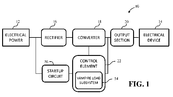
[0026] Figure 1 is a block diagram of a power circuit for use in providing
electrical power to
consumer electronic devices;
[0027] Figure 2-4 are schematic diagrams of the power circuit shown in Figure
1, according to
embodiments of the present invention;
[0028] Figure 5 is another block diagram of the power circuit shown in Figure
1, according to
an embodiment of the present invention;
[0029] Figures 6-8 are schematic diagrams of the power circuit shown in Figure
5, according
to embodiments of the present invention;
[0030] Figure 9 is another block diagram of the power circuit shown in Figure
1, according to
an embodiment of the present invention;
[0031] Figures 10-14 are schematic diagrams of the power circuit shown in
Figure 9, according
to embodiments of the present invention;
[0032] Figure 15 is another block diagram of the power circuit shown in Figure
1, according
to an embodiment of the present invention;
[0033] Figure 16 is another block diagram of the power circuit shown in Figure
15, according
to an embodiment of the present invention;
[0034] Figures 17-19 are schematic diagrams of the power circuit shown in
Figures 15 and 16,
according to embodiments of the present invention;
8
CA 02915376 2015-12-17
[0035] Figure 20-24 are graphic representations of voltage plots associated
with power circuits
shown in Figure 17;
[0036] Figure 25 is a graphic representation of Efficiency vs. Load associated
with the power
circuit shown in Figure 17;
[0037] Figure 26 is another block diagram of the power circuit shown in Figure
1, according
to an embodiment of the present invention;
[0038] Figure 27-41 are schematic diagrams of a BiDFET circuit that may be
used with the
power circuit shown in Figure 26, according to an embodiment of the present
invention;
[0039] Figure 42 is a schematic diagram of a bi-directional field effect
transistor (BiDFET)
that may be used with the power circuit shown in Figures 27-41, according to
an embodiment
of the present invention;
[0040] Figures 43 and 44 are graphic illustrations of the power output of the
bi-directional field
effect transistor shown in Figures 26-42, according to an embodiment of the
present invention;
and
[0041] Figure 45 is a block diagram of a process for manufacturing the power
circuit shown in
Figures 26-42, according to an embodiment of the present invention.
[0042] Corresponding reference characters indicate corresponding parts
throughout the
drawings.
DETAILED DESCRIPTION OF INVENTION
[0043] With reference to the drawings and in operation, the present invention
overcomes at
least some of the disadvantages of known power delivery systems by providing a
power circuit
that provides DC voltage output power to consumer electronic devices from an
AC mains
supply (typically 120VAC (US) to 264VAC[EU/Asia]). The power circuit is
configured to
provide electrical power to charge electronic storage devices and/or power
consumer electronic
9
CA 02915376 2015-12-17
products. The power circuit includes a power converter circuit that includes a
switching device
connected to the primary side of a transformer and a controller that is
coupled to the switching
device to adjust the duty cycle of the switching device to adjust a voltage
level of the output
power to within a desired power specification. In addition, the controller may
adjust the
frequency of the switching device to adjust a voltage level of the output
power. By providing
a switching device such as, for example a MOSFET, -connected to the primary
side of the
transformer, the size of a filter capacitor may be reduced over known
electrical circuits, or
removed.
[0044] The power circuit may also include a quasi-resonant front end, and
synchronous
rectification of the transformer secondary to facilitate reducing switching
and transformer
losses and increase the efficiency of power transfer when charging and/or
powering electronic
devices. In addition, the power circuit includes a vampire load system that is
configured to
determine when a consumer device has finished charging and/or is disconnected
from the
power circuit, and operates the power circuit to disconnect the supply of
power to the power
circuit and/or the electronic device. By providing a power circuit that
includes a greater level
of efficiency over known power circuits and that reduces the occurrence of
vampire loads, wall
wort power, and/or standby power being drawn by the electronic device this
electricity waste,
the amount of electricity used to charge and/or operate consumer electronic
devices is
significantly reduced, thus reducing a cost of operating consumer electronic
products.
[0045] A selected embodiment of the present invention will now be explained
with reference
to the drawings. It will be apparent to those skilled in the art from this
disclosure that the
following description of the embodiment of the present invention is provided
for illustration
only and not for the purpose of limiting the invention as defined by the
appended claims and
their equivalents.
CA 02915376 2015-12-17
[0046] Figure 1 is a block diagram of a power circuit 10 for use in providing
electrical power
to consumer electronic devices. Figure 2-4 are schematic diagrams of the power
circuit 10. In
the illustrated embodiment, the power circuit 10 is configured to receive
power from an
electrical power source 12 and deliver power to an electronic device 14 such
as, for example,
portable consumer electronic devices including, but not limited to, a cell
phone, a smartphone,
a tablet computer, a laptop, and/or any suitable electronic device. In
addition, the power circuit
may deliver power for use in charging electronic storage devices such as, for
example,
mobile phone/laptop/tablet power storage batteries. In one embodiment, the
power circuit 10
may include AC to DC supplies that are designed to provide low voltage DC
output (typically
5VDC) from an AC mains supply (typically 120VAC (US) to 264VAC[EU/Asia]).
These
systems as described below consist of main subsystems, including:
[0047] [1.] Preprocessing, usually using a Full Wave diode bridge and a filter
capacitor to
convert the AC input voltage into a DC voltage.
[0048] [2.] Conversion/Switching, using one of various schemes to convert the
high input
voltage to a much lower output voltage. Often this takes the voltage from DC
to AC.
[0049] [3.] Rectification, re-converting the, AC to DC.
[0050] [4.] Post processing/Output, modifying the output of the conversion
process. This
output is usually an AC voltage which must be changed into a DC output
voltage.
[0051] The power circuit 10 may also include unique combinations of these
subsystems to
produce superior power supplies designed for low voltage battery charging and
other power
supply services from conventional AC mains sources available throughout the
world.
[0052] The conversion process is the central subsystem about which the pre and
post
processing subsystems are wrapped. These subsystems may consist of one of the
following
topologies:
[0053] [1.] Push-Pull
11
CA 02915376 2015-12-17
[0054] [2.] CUK (named after its originator, Slobodan Cuk)
[0055] [3.] SEPIC (Single-ended primary-inductor converter)
[0056] [4.] Buck
[0057] [5.] Flyback
[0058] These subsystems will be described below along with the various pre and
post
processing methods utilized to deliver fully functioning power supply.
[0059] In the illustrated embodiment, the power circuit 10 is configured to
receive input power
of a first type from the electrical power source 12 and deliver output power
of a more desirable
type to the electronic device 14. In one embodiment, the electrical power
source 12 may
include alternating current (AC) input power received from a power grid. For
example, the
electrical power source 12 may include AC input power being delivered at a
given voltage,
e.g., 120 volts and at a frequency of 60 Hertz (the North American Standard)
or 220-240 volts
at a frequency of 50 I-12 (the European Standard). In addition, the power
circuit 10 may be
configured to receive input power having an input voltage within a range
between about 85
volts to 300 volts at either 50 or 60 Hertz so as to accept a world-wide range
of mains power.
In the illustrated embodiment, the power circuit 10 is configured to convert
the AC input power
to a more desirable direct current (DC) output power. For example, in one
embodiment, the
power circuit 10 is configured to deliver DC output power at the desired
voltage, such as 5
volts direct current (VDC). In the illustrated embodiment, the power circuit
10 is configure to
receive input power from the electrical power source having an AC power signal
at a first
voltage level and delivering an output power signal having a DC power signal
at a second
voltage level that is less than the first voltage level. For example, in one
embodiment, the
power circuit 10 is configured to receive input power at 120 volts AC at a
frequency of 60
Hertz and deliver output power at 5 volts DC.
=
12
CA 02915376 2015-12-17
[0060] In the illustrated embodiment, the power circuit 10 includes a
rectifier circuit 16 that is
coupled to the electrical power source 12, a power converter circuit 18 that
is electrically
coupled to rectifier circuit 16, an output section 20 that is coupled to the
power converter circuit
18 for delivering power from the power converter circuit 18 to the electronic
device 14, and a
control element 22 for operating the power converter circuit 18 to deliver
power to the output
section 20 at a desired power signal.
[0061] In one embodiment, the rectifier circuit 16 is configured to generate a
modified AC
power signal from the AC input power received from the electrical power source
12. The
power converter circuit 18 is configured to receive the modified AC power
signal at an input
voltage level from the rectifier circuit 16 and generate a DC output power
signal at an output
voltage level that is less than the input voltage level. More specifically,
the rectifier circuit 16
receives the AC input power signal at the input voltage level from the power
source 12 and
generates the modified AC power signal. The control element 22 operates the
power converter
circuit 18 to reduce the input voltage level and generate the DC output power
signal at the
desired output voltage level from the received modified AC power signal.
[0062] The output section 20 includes an appropriate power connecter or port,
such as a
universal serial bus (USB) port, that is configured to electrically couple the
electronic device
14 to the power circuit 10 to facilitate delivering power from the power
circuit 10 to the
electronic device 14.
[0063] The rectifier circuit 16 is configured to receive an AC input power
from the electrical
power source 12 and deliver DC input power to the power converter circuit 18.
In the illustrated
embodiment, the rectifier circuit 16 includes a plurality of diodes that are
arranged in a full-
wave bridge rectifier 24 having first and second input terminals coupled to
the high and low
sides of the electrical power source 12 for producing a DC power signal from
an AC input
power signal. In one embodiment, the rectifier circuit 16 may also include a
filter capacitor 26
13
11
CA 02915376 2015-12-17
that is coupled to the full-wave bridge rectifier 24. In another embodiment,
the rectifier circuit
16 may include a half-bridge rectifier (not shown). In yet another embodiment,
the rectifier
circuit 16 does not include the filter capacitor 26.
[0064] In the illustrated embodiment, the power converter circuit 18 receives
the DC input
power from the rectifier circuit 16 and delivers a DC output power to
electronic device 14 via
the output section 20. In one embodiment, the power circuit 10 does not
include the rectifier
circuit 16 and the power converter circuit 18 is coupled to the electrical
power source 12 for
receiving AC input power from the electrical power source 12 and delivering DC
output power
to the electronic device 14.
[0065] Referring to Figure 2, in one embodiment, the power converter circuit
18 includes a
modified cuk converter 28. In contrast to known non-isolated and isolated cuk
converters that
are used for DC-DC conversions, the modified cuk converter 28 is configured
for AC-DC
conversions using rail voltage which is reduced down to, for instance, 5V at
the desired current.
The modified cuk converter 28 includes a high frequency transformer 30, and a
switching
device 32 coupled to a primary side of the transformer 30. In the illustrated
embodiment, the
switching device 32 includes an inductor 34, a main field-effect transistor
(FET) 36 on the top
side of the transformer 30, and a capacitor 38 as the main energy-storage
component. In one
embodiment, the FET 36 may be a metal¨oxide¨semiconductor field-effect
transistor
(MOSFET). In addition, the FET 36 may include an N-channel MOSFET and/or a P-
channel
MOSFET. The modified cuk converter 28 also includes an asynchronous
rectification circuit
40 connected to the secondary side of the transformer 30. The asynchronous
rectification
circuit 40 may include a capacitor, a diode, and an inductor.
[0066] In the illustrated embodiment, the control element 22 includes a
controller 42 that is
coupled to the main FET 36 and a sensing circuit 44 that is coupled to the
transformer 30 for
sensing an output voltage level of power being generated by the transformer
30. In one
14
CA 02915376 2015-12-17
embodiment, the sensing circuit 44 includes a diode, a capacitor, and a
resistor. The controller
42 is configured to receive the sensed voltage from the sensing circuit 44 and
transmit a control
signal to the switching device 32 to operate the switching device 32 to adjust
a voltage level of
output power being delivered from the power converter circuit 18 to the
electronic device 14.
In one embodiment, the controller 42 includes a microprocessor that is
programmed to receive
the sensed voltage level from the voltage sensor and transmit a control signal
to the switching
device 32 to adjust the voltage level of power being delivered to the
electronic device 14. The
controller 42 may also implement a pulse-width modulation (PWM) process to
operate the
switching device 32 to adjust the voltage level of the output power signal.
[0067] In the illustrated embodiment, the modified cuk converter 28 control is
identified as
Vout/Vin = duty cycle / (period - duty cycle), which is used by the controller
42 to drive the main
FET included in the switching device 32. Moreover, the controller 42 is
configured to adjust
=a duty cycle of the control signal to adjust a voltage level of the output
power. The sensing
circuit 44 provides feedback to the controller 42 so that if the output
voltage is too low, the
controller 42 increases the duty cycle of the control signal and the FET 36.
Conversely, if the
voltage is too high the duty cycle is decreased. Another advantage of the
modified cuk
converter 28 is that the relation between the output and input voltage is D/(1-
D), where D is
the duty cycle. For a given transformer 30, the output voltage may be
increased or decreased
as required so that Dial-A-Voltage features may apply. Also, because of the
relationship of the
input to output voltage with respect to the duty cycle, the output voltage can
be adjustable.
[0068] Referring to Figure 3, in one embodiment, the power converter circuit
18 includes a
modified SEPIC converter 46. Known SEPIC converters are known to be used for
DC-DC
rectification. In contrast to known SEPIC converters, the modified SEPIC
converter 46 is
configured for AD-DC conversions. The modified SEPIC converter 46 is
configured to enable
CA 02915376 2015-12-17
a method of operation that provides that the electrical potential (voltage) at
its output to be
greater than, less than, or equal to that at its input.
[0069] In the illustrated embodiment, the modified SEPIC converter 46 includes
a high
frequency transformer 30 and a switching device 32 that is coupled to a
primary side of the
transformer 30. The switching device 32 includes an inductor 34, a main FET 36
on the top
side of the transformer 30, and a capacitor 38. The modified SEPIC converter
46 also includes
an asynchronous rectification circuit 40 that includes a diode connected to
the secondary side
of the transformer 30. The modified SEPIC converter 46 is operated to convert
AC to DC
using rail (mains) power and convert it down to a desired voltage, such as 5V
at a desired
current, such as 10 to 12A.
[0070] The control element 22 includes the controller 42 that is coupled to
the switching device
32 and the sensing circuit 44 for sensing an output voltage level of power
being generated by
the transformer 30. The output of the modified SEP1C converter 46 is
controlled by the duty
cycle of the control transistor. The control is accomplished by Vout/Vin =
duty cycle / (period -
duty cycle). The main FET 36 is driven by the controller 42 in the modified
SEPIC converter
46 to adjust a voltage level of the output power being delivered to the
electronic device 14. In
addition, the sensing circuit 44 provides feedback to the controller 42 to
enable the controller
42 to adjust a duty cycle of the control signal being transmitted to the main
FET 36 to adjust
an output voltage of the transformer 30. For example, if the sensed output
voltage is too low,
the controller 42 increases the duty cycle of the control signal to increase
the output voltage
level. Conversely, if the voltage is too high the duty cycle is decreased.
[0071] For the modified SEPIC converter 46, the current through the main FET
Q1 in the
modified SEPIC converter 46 is approximately equal to the sum of the input
current as well as
the output current. The modified SEPIC converter 46 includes minimal switches
similar to the
modified cuk converter 28, but the current through the MOSFET Q1 is reduced.
This is
16
CA 02915376 2015-12-17
because the secondary load current is prevented from flowing through Q1 by the
way diode D3
is positioned. This reduces the I2R heating loss in MOSFET Ql.
[0072] In one embodiment, as shown in Figure 14, the power converter circuit
18 may include
a modified Buck converter 47.
[0073] Referring to Figure 4, in one embodiment, the power converter circuit
18 may include
a modified Push-Pull converter 48. Known Push-Pull conversion topology has
been known in
the industry and is exclusively used for DC-DC conversions. In contrast to
known Push-Pull
topologies, the modified Push-Pull converter 48 is configured for AC-DC
conversion from rail
voltages down to 5V capable of producing 10 to 12 Watts. In one embodiment,
the modified
Push-Pull converter 48 includes a high frequency transformer 30. In addition,
the primary side
of the transformer 30 is center tapped with the rectified high voltage
attached to the center tap.
In addition, the modified Push-Pull converter 48 includes a switching device
32 that includes
a pair of FETs 36 arranged 180 degrees out of phase with respect to each
other, and that
alternate pulling the current through the each side of the primary winding
(hence the name
push-pull) of the transformer 30. Since the magnetic flux switches direction
with the push pull,
the voltage on the secondary will also switch direction. Therefore, a center
tapped secondary
is used because when the flux is flowing in one direction the top half of the
secondary will be
positive. Likewise, when the flux reverses, the lower side will produce a
positive voltage. The
modified Push-Pull converter 48 may also include an asynchronous rectification
circuit 40 that
includes a pair of diodes, D1, D3, connected to the secondary side of the
transformer 30. The
diodes are configured as a clamping mechanism to prevent the backflow of
electricity from the
transformer, and may include a super barrier diode, due to its high blocking
abilities, with low
energy losses.
[0074] The modified Push-Pull converter 48 includes FETs 36 on either side of
the transformer
primary that are configured to be pulled low by the PWM process at opposite
times. The
17
=
CA 02915376 2015-12-17
controller 42 transmits control signals to each of the FETs 36 to operate the
modified Push-
Pull converter 48 to control the power circuit 10 as follows: the FETs 36 on
either side of the
transformer primary will be pulled low by the PWM process at opposite times.
When the
output voltage falls below a certain threshold the first FET Q1 will turn on
for a fixed time and
then turn off. Next, after a predetermined dead time, the second FET Q2 will
turn on for a
fixed time and then turn off. After the second FET Q2 turns off, the system
enters a rest time
relative to the output current desired or the time needed to transfer enough
energy to the load
to cause the output voltage to drop below a certain threshold (the higher the
current, the rest
time reduces, and the lower the output current, the greater the rest time).
The process would
repeat when the secondary side voltage decreased below the threshold. In
addition, the
controller 42 receives the sensed voltage from the sensing circuit 44 and
transmits a control
signal to each of the FETs 36 to adjust a voltage level of output power being
delivered from
the power converter circuit 18 to the electronic device 14.
[0075] In one embodiment, as shown in Figure 4, the sensing circuit 44 may
include a sensor
50 connected to the asynchronous rectification circuit 40 and/or the
transformer secondary for
sensing a voltage level and/or a current level of the output power signal
being delivered to the
electronic device 14 from the power converter circuit 18. In one embodiment,
the sensor 50
includes a resistor that is coupled to the controller 42 for transmitting a
signal indicative of
power characteristics associated with the output power. The controller 42 may
be configured
to determine a voltage level of the output power as a function of the received
signal. In another
embodiment, the controller 42 may determine a current draw of the electronic
device 14 as a
function of the sensed signal. Moreover, the controller 42 may be configured
to adjust a duty
cycle of the control signals being transmitted to the power converter circuit
18 as a function of
the sensed power characteristic.
18
CA 02915376 2015-12-17
[0076] In one embodiment, the controller 42 may be configured to detect an
initial current
draw from the electronic device 14 as a function of the signal being received
from the sensing
circuit 44 and responsively initiate a charging cycle including operating the
power circuit 10 to
deliver output power to the electronic device 14. In addition, the controller
42 may monitor a
level of current being drawn by the electronic device 14 during the charging
cycle and detect
if the monitored level of current being drawn by the electrical device is
different than a
threshold level of current. The controller 42 may also determine a voltage
level of power being
delivered to the electronic device 14 as a function of the signals being
received from the sensing
circuit 44 and transmit a control signal to the power circuit 10 to adjust the
voltage level of
power being delivered to the electrical device. In one embodiment, the
controller 42 may adjust
a duty cycle of the control signal being transmitted to the power circuit 10
to adjust the voltage
level of power being delivered to the electrical device. Moreover, the
controller 42 may adjust
the duty cycle of the control signal to maintain the monitored voltage level
within a predefined
voltage range.
[0077] In one embodiment, the controller 42 generates a control signal that is
a variable
frequency. The frequency of the control signal is modified to deliver the
desired output power.
The switching device 32 receives a control signal from the control element 22
and converts the
DC voltage output of the rectifier circuit 16 into an alternating current
power signal. The
frequency of the alternating current power signal is responsive to the control
signal. Moreover,
the frequency of the control signal from the control element 22 controls the
frequency of the
alternating current power signal. Based on the sensed voltage and current
delivered, the control
element 22 may modify the frequency of the control signal to fine tune and
more accurately
control the output of the power circuit 10. For example, in one embodiment,
the controller 42
monitors the output power signal and adjusts the control signals to the
switching device 32 to
keep the power output within specification. The controller 42 may also include
an associated
19
CA 02915376 2015-12-17
control program that may compensate for different output load conditions,
component
tolerances, component parameter variations at different operating points, and
component
changes due to temperature. The control program also monitors several
operating parameters
to turn the switching device off, which removes power from the output, if a
condition that is
unsafe or out of the operating range is detected.
[0078] In one embodiment, the controller 42 includes software to enable the
controller 42 to
recognizes through its logic in the microprocessor the draw from the battery
as connected and
analyzes the ramp up draw from that battery and then either sends 1 A (for
charging a cell
phone) or up to 2.4 A for devices like a tablet; or up to 9.2 A for charging a
notebook or laptop,
which the current invention can either do alternatively or at the same time.
In one embodiment,
the acceptable input voltage can range from a low of 85V ¨ a high of 300V
worldwide. Output
voltage is device dependent but 5V to 19V are possible.
[0079] In the illustrated embodiment, the sensing circuit 44 includes an
electrical isolation
device 52 connected between the controller 42 and the sensor 50. The
electrical isolation
device 52 may include, but is not limited to, a transistor, an opto
transistor, an opto triac, and/or
any suitable electrical isolation device.
[0080] In one embodiment, the control element 22 may include a vampire load
subsystem 54
that is configured to monitor the output power being delivered to the
electronic device 14 and/or
to monitor a current draw of the electronic device 14 to determine if the
electronic device is
powered by, being charged and/or is attached to the power circuit 10. The
vampire load
subsystem 54 may include synchronous switching at high voltage subsystem that
includes a
synchronous switch matrix that may increase efficiency during high current
operation and
provides the opportunity for significantly reduced idling power as well.
During operation, the
controller 42 may monitor the output power to determine if a device was being
charged or is
CA 02915376 2015-12-17
attached to the power circuit 10, and disconnect the power circuit 10 from the
electrical power
source 12 upon determining that the electronic device 14 is no longer being
charged.
[0081] For example, in one embodiment, the controller 42 is configured to
receive a signal
from the sensing circuit 44 that is indicative of current being drawn by the
electronic device
14, detect an initial current draw from the electrical device as a function of
the received signal,
and responsively initiate a charging cycle and responsively deliver output
power to the
electronic device 14 via the power circuit 10. The controller 42 may also
monitors a level of
current being drawn by the electronic device 14 during the charging cycle,
detects if the
monitored level of current being drawn by the electrical device is less than a
threshold level of
current, and responsively operates the power circuit 10 to disconnect power to
the electronic
device 14. The controller 42 may also determine that the electronic device 14
is disconnected
from the power circuit if the monitored level of current is less than the
threshold level of
current. In one embodiment, power for the control and monitor would be stored
in an on-board
capacitor and a timer that would allow the circuit to periodically wake up,
power up the system,
and determine whether to keep it powered up. This duty cycle would result in a
significant
reduction in average quiescent power (the power wasted when no device is being
charged).
[0082] In one embodiment, the vampire load subsystem 54 may determine a level
of charge
being held in a output supply capacitor 55 and determine whether the
electronic device 14 is
connected to the power circuit, being charged by the power circuit 10, and/or
being powered
by the power circuit 10 as a function of level of charge being held in the
output supply capacitor
55. For example, in one embodiment, the sensing circuit 44 may sense a voltage
across the
output supply capacitor 55 and disconnect the power being supplied to the
electronic device 14
if the sensed voltage is different than a threshold voltage. The vampire load
subsystem 54 is
configured to determine if the sensed voltage is different than a threshold
voltage level and
operate the power converter circuit to disconnect power to the electronic
device. For example,
21
CA 02915376 2015-12-17
in one embodiment, the vampire load subsystem 54 determines if the sensed
voltage is less
than a threshold voltage, e.g. 5 volts, and responsively determine that the
electronic device 14
is being charged by the power circuit 10, and/or being powered by the power
circuit 10. In
addition, if the sensed load is greater than, or equal to, the threshold
voltage level, the vampire
load subsystem 54 may responsively determine that the electronic device 14 is
not drawing
power from the power circuit and responsively operate the power circuit 10 to
disconnect the
delivery of power to the electronic device 14.
[0083] The controller 42 and sensing circuit 44 continually monitor the draw
of current from
the charging device. From the initiation of the charging cycle, a table is
formed in the controller
42 for use in analyzing the current draw. During the charging cycle the
controller 42 continues
to monitor the current draw that is being consumed by the electronic device 14
via the sensing
circuit 44 and analyzes that draw and reports when the draw begins to wane due
to a fully
charged device. The controller 42 may also sense when the current diminishes
as the charging
device approaches a full charge. From the initial outrush of current to the
charging device
through the entire charging cycle, the controller 42 determines when a
charging device is fully
or nearly fully charged (and when the current draw approaches zero), and shuts
off power from
its inrush supply and shuts down the charging and power draw from the inrush
source. The
controller 42 may also detect when a device is connected to the power circuit
10 by sensing the
current draw. At any time when there is no current draw, the controller 42
operates power
circuit 10 to shut off, avoiding the ongoing electrical waste that normally
exist when a charging
device is still plugged into a wall outlet, but no phone is attached.
[0084] In the illustrated embodiment, the power circuit 10 includes a startup
circuit 56 that is
connected to the control element 22 for providing start-up power to the
controller 42. The high
voltage diode bridge is a potentially significant opportunity to place the
vampire load
subsystem 54, since a diode bridge is passive. When power is off and then is
turned on (when
22
CA 02915376 2015-12-17
the power supply is plugged into the socket), the bridge begins conducting
power into the
system automatically. The main issue with having a synchronous switch
configuration at the
line interface is the chicken-egg problem. Switches must be actively
controlled. Active control
requires power, but power may not be available until the switches are actively
turned on. The
startup circuit 56 may facilitate the start-up issue and may include a
separate, extremely simple,
low power regulator circuit that is configured to provide just enough power to
the controller 42
for the monitor and switch matrix controller to function. Being simple, this
regulator would not
be very efficient. However, it would be sized for very low power and therefore
any inefficiency
would be relatively unimportant, and it would be disconnected (turned off)
once the main
power supply chain and microprocessor is on-line, further reducing energy
loss.
[0085] The control element 22 may also include separate primary and secondary
monitor and
switch controller sections of circuitry. The secondary would be the one
powered continuously
whenever the power supply was plugged in. The primary would maximize the
efficiency of the
system during charging. Its performance might need to be superior to that of
the secondary,
whose purpose is only to operate when the unit is first plugged in.
[0086] Figure 5 is another block diagram of the power circuit 10, according to
an embodiment
of the present invention. Figure 6-8 are schematic diagrams of the power
circuit 10. In the
illustrated embodiment, the power circuit 10 includes a synchronous
rectification circuit 60
that is connected to the power converter circuit 18 for use in rectifying the
output power signal
being delivered to the electronic device 14. The synchronous rectification
circuit 60 includes
a synchronous switching device 62 that is coupled to the transformer secondary
and a
synchronous control device 64 that is coupled to the synchronous switching
device 62. The
synchronous control device 64 is connected to the controller 42 and is
configured to receive a
synchronization control signal from the controller 42 and generate a switch
control signal as a
function of the received synchronization control signal to operate the
synchronous control
23
CA 02915376 2015-12-17
device 64 to rectify the output signal received from the transformer 30. In
one embodiment,
the controller 42 is configured to adjust a duty cycle of transistor control
signal as a function.
of the sensed transformer voltage level and/or the voltage level of the output
power delivered
to the electronic device 14. In the illustrated embodiment, the synchronous
rectification circuit
60 includes an electrical isolation device 52 connected between the
synchronous control device
64 and the controller 42.
[0087] In one embodiment, the synchronous switching device 62 may include a
FET 36 that is
connected to the secondary side of the transformer 30. The synchronous control
device 64 is
coupled to the FET 36 to rectify the power output signal being delivered to
the electronic device
14 from the transformer 30. For example, as shown in Figure 6, the power
circuit 10 may
include the modified cuk converter 28 with the synchronous rectification
circuit 60 including
a synchronous FET 36 connected to the transformer secondary. In addition, as
shown in Figure
7, the power circuit 10 may include the modified SEPIC converter 46 with the
synchronous
rectification circuit 60 including a synchronous FET 36 connected to the
transformer
secondary.
[0088] In another embodiment, as shown in Figure 8, the synchronous switching
device 62
may include a pair of synchronous 1-1,Ts 36 that are connected to the
secondary side of the
transformer 30. For example, the power circuit 10 may include the modified
Push-Pull
converter 48 with the synchronous rectification circuit 60 including a pair of
synchronous FETs
36 on the transformer secondary to control the flow from each half of the
secondary winding
so that current from the output flows only one way producing a DC output. The
synchronous
FET(s) is(are) turned on by the controller when the voltage across the FET
will allow current
to flow to the output of the converter, and is(are) turned off to block the
flow of current back
through the converter, preventing current to backflow to the transformer. In
the modified Push-
24
CA 02915376 2015-12-17
Pull converter 48 (shown in Figure 8), the FET(s) replace diodes and provide
increased
efficiency as the Ron features of a FET provide a lower power loss than a
diode.
[0089] In one embodiment, as shown in Figure 14, the power circuit 10 includes
a synchronous
rectification circuit 60 connected to the primary side of the transformer 30
in place of, or in
addition to, the full-wave bridge rectification circuit 24. The primary side
synchronous
rectification circuit 60 may include a synchronous switching device 62 that
includes four
synchronous FETs 36. In one embodiment, the synchronous switching device 62
may include
a single synchronous FET 36, a pair of synchronous FETs 36, or any suitable
number of FETs
36 connected to the transformer primary side. By providing the rectification
circuit 16
including a synchronous rectification circuit 60, the size of the filter
capacitor 26 may be
reduced over known electrical circuits, or the filter capacitor 26 may be
removed from the
power circuit 10.
[0090] Figure 9 is another block diagram of the power circuit 10, according to
an
embodiment of the present invention. Figures 10-14 are schematic diagrams of
the power
circuit 10. In the illustrated embodiment, the power circuit 10 includes a
quasi-resonant circuit
66 that is coupled to the power converter circuit 18. The quasi-resonant
circuit 66 includes a
switching device 68 that is coupled to the controller 42, a diode 70 that is
coupled to the
switching device 68, an inductor 72 coupled to the diode 70, and a capacitor
74 that is coupled
to the inductor 72. In one embodiment, the switching device 68 may include a
FET 36. In one
embodiment, the quasi-resonant circuit 66 does not include an inductor 72
and/or a diode 70.
In another embodiment, the quasi-resonant circuit 66 does not include the
switching device 68.
[0091] In the illustrated embodiment, the controller 42 is configured to
determine a zero
crossing of the transformer 30 as a function of the sensed transformer voltage
and operate the
switching device 68 to deliver input power to the primary side of the
transformer 30 as the
transformer 30 approaches the zero crossing. In addition, the controller 42
may also monitors
CA 02915376 2015-12-17
a level of current being drawn by the electronic device 14 during the charging
cycle, detects if
the monitored level of current being drawn by the electrical device is less
than a threshold level
of current, and responsively operates the power circuit 10 to disconnect power
to the electronic
device 14. In one embodiment, the controller 42 may operate the one or more
FETs 36 included
in the switching device 32, the quasi-resonant circuit 66 and/or the
synchronous switching
device 62 to disconnect power from the electrical power supply 12 and/or the
electronic device
14.
[0092] As shown in Figures 10-14, each of the modified cuk converter 28, the
modified SEPIC
converter 46, the modified Buck converter 47, and/or the modified Push-Pull
converter 48 may
include the quasi-resonant circuit 66. In one embodiment, the quasi-resonant
circuit 66 may
include a FET, diode, and LC circuit that are placed on the front end to allow
the main switching
elements to fully turn while the current passing through them is "zero" or
similar. The FET in
the quasi-resonant circuit 66 provides an oscillation to allow the main FET(s)
included in the
power converter circuit 18 to switch at zero current to reduce switching
losses. Unlike a linear
power supply, the quasi-resonant circuit 66 includes regulation that uses a
pass transistor of a
switching-mode supply which continually switches between low-dissipation, full-
on and full-
off states, and spends very little time in the high dissipation transitions,
which minimizes
wasted energy. Ideally, a switched-mode power supply dissipates no power.
Voltage regulation
is achieved by varying the ratio of on-to-off time. In contrast, a linear
power supply regulates
the output voltage by continually dissipating power in the pass transistor.
This higher power
conversion efficiency is an important advantage of a switched-mode power
supply. Switched-
mode power supplies may also be substantially smaller and lighter than a
linear supply due to
the smaller transformer size and weight.
[0093] Referring to Figures 13 and 14, in one embodiment, the control element
22 includes
one or more Hall Effect sensors 76 that are coupled to the transformer 30 for
sensing a magnetic
26
CA 02915376 2015-12-17
field being generated within the transformer 30. The Hall Effect sensors 76
facilitate
determining a zero-crossing of the transformer 30 by directly sensing the
magnetic field being
generated by the transformer 30 during operation. In one embodiment, the
control element 22
include a primary side Hall Effect sensor 76 coupled to the primary side of
the transformer 30.
The primary side Hall Effect sensor 76 is connected to the controller 42 for
transmitting a signal
to the controller 42 for use in determining when the transformer 30 nears the
"zero-crossing".
In another embodiment, the control element 22 includes a secondary side Hall
Effect sensor 76
that is coupled to the secondary side of the transformer 30, and is connected
to the synchronous
control device 64 for transmitting a signal indicative of the transformer
magnetic field for use
in determining the time at which the transformer 30 reaches the "zero-
crossing".
[0094] Figures 15 and 16 are additional block diagrams of the power circuit
10, according to
an embodiment of the present invention. Figures 17-19 are schematic diagrams
of the power
circuit 10. In the illustrated embodiment, the power circuit 10 includes a
bridge rectifier 80,
an energy well transformerless converter 82, and a high efficiency buck
converter 84. The
bridge rectifier 80 receives AC input power and delivers DC input power to the
energy well
transformerless converter 82. The energy well transformerless converter 82
receives the DC
input power at a voltage level and delivers a DC output power at a lower
voltage level to the
buck converter 84 for delivery to the electronic device 14. In one embodiment,
the energy well
transformerless converter 82 delivers power to the buck converter 84 at a
first voltage level and
the buck converter 84 delivers the DC output power to the electronic device 14
at a second
voltage level that is less than the first voltage level. For example, as shown
in Figure 18, the
energy well transformerless converter 82 may receive an input power at an
input voltage, Vin
equal to about 311VDC, and deliver an output power at a output voltage, Vout
equal to about
25 VDC. The buck converter 84 may receive the output power at 25 VDC and
deliver output
power to the electronic device 14 at an output voltage of about 5VDC.
27
CA 02915376 2015-12-17
[0095] In the illustrated embodiment, the energy well transformerless
converter 82 includes a
modified Dickson charge pump including a plurality of voltage reduction energy
wells 86 for
use in reducing a voltage of an input power signal. Each energy well 86
includes one or more
capacitors 88 which are set in ranges of different voltages in any voltage
division, from very
small to large (i.e. 0.10V, 1V, 5V, and etc.). Switching devices 90, such as,
for example
MOSFETs, are connected to the energy wells 86. In one embodiment, the switches
devices 90
may be configured to withstand a 1/N of voltage swing, VDS and/or a 2/N
voltage swing. In
the illustrated embodiment, the power circuit 10 may also include a high side
controller 92 and
a low side controller 96 to facilitate operating the power circuit 10.
[0096] In one embodiment, the energy well transformerless converter 82 may
also include a
floating gate drive 96 that is connected to one or more stacks and/or stages
of energy wells 86.
In addition, the floating gate drive 96 may include a first set 98 of MOSFETs
and diodes and a
second set 100 of MOSFETs and diodes that are connected via a cross-coupling
converter.
[0097] In one embodiment, as shown in Figure 16, the power circuit 10 may
include a high
efficiency synchronous rectifier 102 that is connected to the energy well
transformerless
converter 82. In addition, the power circuit 10 may also include a high side
smart controller
104 for use in controller the synchronous rectifier 102, and a low side smart
controller 106 for
use in controlling an operation of the buck converter 84.
[0098] Figure 20-24 are graphic representations of voltage plots associated
with the power
circuit 10 including the energy well transformerless converter 82. Figure 25
is a graphic
representation of Efficiency vs. Load associated with the power circuit 10
shown in Figure 17.
The illustrative plots shown in Figures 20-25 are generated during a
simulation of the power
circuit 10 under the following parameters: clkperiod = 3.5e-007; clkcycles =
50000; switchRon
= 1; ci = le-006; Vin = 311; and lout = 1.2A.
28
=
CA 02915376 2015-12-17
[0099] Figure 26 is another block diagram of the power circuit 10 including
the power
converter circuit 18 including a bi-directional field effect transistor
(BiDFET) circuit 120,
according to an embodiment of the present invention. Figures 27-41 are
schematic diagrams
of a BiDFET circuit 120 that may be used with the power circuit 10. Figure 42
is a schematic
diagram of a BiDFET 122 that may be used with the BiDFET circuit 120. In the
illustrated
embodiment, the BiDFET circuit 120 includes one or more BiDFETs 122 that are
connected
to a transformer 124. In one embodiment, the transformer 124 includes high-end
tap 126, a
center tap 128, and a low-end tap 130. The power circuit 10 may also include
three BiDFETs
122 that are connected to each of the high-end tap 126, a center tap 128, and
a low-end tap 130.
The transformer 124 is center tapped, such that with the three BiDFETs 122
either as separate
components or built as integrated into a single IC's permitting the conversion
from either
240/260VAC can be made (using the top tap on the transformer), and the
conversion from
110/120VAC can be made by utilizing the center tap on the transformer. As
shown in Figures
28 and 29, one of the BiDFETs 122, is a "common" BiDFET and the other two
BiDFETs 122
are configured to receive inputs from both 110AC and 240AC, respectively. The
power circuit
is configured to operate the BiDFETs 122 to receive input power at varying
voltage levels.
For example, the power circuit 10 may include a 110VAC BiDFET 122 placed on
the center
tap 128, a 240 VAC BiDFET 122 at the high-end tap 126, and a common BiDFET 122
or
ground on the low-end tap 130 of the transformer 124. This enables the power
circuit 10 to
generate the DC output power signal having a output voltage level (i.e. 6VAC)
at the same
current regardless of which mains voltage is selected (110VAC/240VAC). In
another
embodiment, the BiDFET circuit 120 may include two BiDFETs 122 (shown in
Figure 27) that
are connected to the center tap 128 and the high-end tap 126. In addition, the
BiDFETs 122
may also be used with transformerless circuits such as, for example, the power
circuit 10 shown
in Figures 15 and 16.
29
CA 02915376 2015-12-17
[00100] Referring to Figure 42, in the illustrated embodiment, each BiDFET 122
includes two
field effect transistors (FET) 132 that are connected in parallel back to
back. In one
embodiment, the BiDFET 122 includes one or more diodes 134 in their respective
drains. The
FETs 132 are selected as a function of a suitable breakdown voltage such as
650 volts for units
designed to operate in a 120 VAC or 240VAC environment. The diodes 134 are
selected with
the same breakdown voltage as the FETs 132. In addition, the diodes 134 are
connected to the
respective drains of each FET 132 and may be connected to the sources instead
of drains. The
diodes 134 are configured to protect the corresponding FET 132 from the high
reverse voltage
that could be extant via the AC inputs half cycle that is opposite of the
BiDFETs 122 normal
operating voltage. In one embodiment, the BiDFET 122 may include two MOSFETS
back to
back pointed in the opposite direction with each half of the BiDFET 122 having
a forward
biased diode in series with the drain. The point of the diode, if not
incorporated into the
BiDFET 122, is to protect the BiDFET 122 when there exist high level reverse
voltages. In
another embodiment, the BiDFET 122 may include an opto triac and/or two SCR's
back to
back. The opto triacs may be configured to vary the signal frequency, switch
at high speeds,
and be "turned-off". In another embodiment, the BiDFET circuit 120 may include
a
combination BiDFET layout that includes one diode 134 attached to one of the
BiDFET's drain
with the other diode 134 placed off the source of the companion BiDFET 122.
[00101] In the illustrated embodiment, the BiDFET 122 is configured to be
normally used in
any location within the power circuit 10 that a Triac might be used, with the
added advantage
that the BiDFET 122 can be turned off. Thus, the BiDFET 122 does not have two
drawbacks
that Triacs possess. The BiDFET 122 can switch at high operating frequencies
and may be
turned off unlike Triacs which, when once turned on, can only turn off when
the applied voltage
is reduced to zero.
CA 02915376 2015-12-17
[00102] Figure 29 is a schematic diagram of the BiDFET circuit 120 including a
multi-tap
transformer. Figure ,30 is a schematic diagram of the BiDFET circuit 120
including the
BiDFET with FET source connected to the AC main, asynchronous secondary, and
PWM
controller referenced to secondary. Figure 31 is a schematic diagram of the
BiDFET circuit
120 including an asynchronous BiDFET with FETs blocking current from. the
transformer.
Figure 32 is a schematic diagram of the BiDFET circuit 120 including the
BiDFET with single
side switching. Figure 33 is a schematic diagram of the BiDFET circuit 120
including the
BiDFET with FET source connected to the transformer, synchronous secondary,
and PWM
controller referenced to secondary. Figure 34 is a schematic diagram of the
BiDFET circuit
120 including the BiDFET with FET source connected to the transformer and PWM
controller
referenced to asynchronous secondary. Figure 35 is a schematic diagram of the
BiDFET circuit
120 including the BiDFET with FET source connected to the transformer,
synchronous
secondary, and PWM controller referenced to primary. Figure 36 is a schematic
diagram of
the BiDFET circuit 120 including the BiDFET with FET source connected to the
transformer,
asynchronous secondary, and PWM controller referenced to primary. Figure 37 is
a schematic
diagram of the BiDFET circuit 120 with asynchronous BiDFET with FETs blocking
current
from AC source. Figure 38 is a schematic diagram of the BiDFET circuit 120
including the
BiDFET with FET source connected to the AC main, synchronous secondary, and
PWM
controller referenced to primary. Figure 39 is schematic diagram of the BiDFET
circuit 120
including synchronous BiDFET with FETs blocking current from the transformer.
Figure 40
is a schematic diagram of the BiDFET circuit 120 including the BiDFET with FET
source
connected to the AC main and PWM controller referenced to synchronous
secondary. Figure
41 is a schematic diagram of the BiDFET circuit 120 including the BiDFET with
FET source
connected to the AC main, asynchronous secondary, and PWM controller
referenced to
primary.
31
CA 02915376 2015-12-17
[00103] In one embodiment, the BiDFET 122 does not include a diode and
includes an 'N'
channel FETs 132 that opposes the current on the high side of the transformer
124 and a diode
134 (shown in Figures 30 and 31) on the low side of the transformer 124 (and
similarly for the
other half of the wave). As shown in Figures 30 and 31, during operation,
during the positive
half of the wave FET Q1 is toggled at the switching frequency and FET Q2 is on
and serves as
a forward biased diode. In addition, a reverse biased FET can't be turned off
because of the
forward biased body diode, but it can be turned on even with current flowing
backwards. So,
if the FET is turned on then the result is a very small resistor in parallel
with the diode so that
as long as the RDs(oN) is lower than the effective resistance of the diode the
diode drop is
effectively removed as well, improving efficiency. In another embodiment, for
increased
efficiency, D1 and D2 are replaced with synchronous FETS (as shown in Figure
33).
[00104] Referring to Figures 43 and 44 during operation, the BiDFET circuit
120 is configured
to "chop up" a low frequency (50 ¨ 60 cycle) AC voltage into much smaller
segments by
operating at a much higher frequency. For example, during operation an input
AC power signal
may be chopped into much finer pieces at a rate equal to about 50 to 60 Khz,
or up to 1Mhz or
more if the switch losses are low enough to warrant such a faster chop rate. A
higher BiDFET
switching rate leads to smaller parts but higher switching losses. In
addition, an operation of
the BiDFET circuit 120 may be optimized to operate at an efficient frequency
using the Ron
features of the BiDFET circuit 120.
[00105] Figure 43 illustrates a "chopped" frequency wave generated by the
BiDFET circuit
120 demonstrating that the BiDFET chops both the positive and negative
segments of the sign
wave. In addition, the control element 22 includes a PWM protocol enables the
BiDFET to
generate the "chops" narrow at the highest voltage and "fatter" closer to the
zero point crossing,
where the least energy exists in AC waveform. This minimizes the pulsating
effect inherent in
these chops on both the positive and negative segments of the sign wave.
32
CA 02915376 2015-12-17
[00106] In the illustrated embodiment, the power circuit 10 includes a high-
speed AC switch,
operated by a PWM signal from the control element 22 slicing both the positive
and negative
segments of a 50/60 sine wave. However, the BiDFETs are not limited to any
specific
frequency and could manage any given frequency at the right controller speed.
In addition, in
one embodiment, the BiDFETs 122 may be operated similar to fast Triacs (which
are also AC
switches but operate at relatively low speeds). The BiDFhT 122 is a high-speed
switcher
including switching speeds within a range between about 501(z-1MHz, and/or
greater than
1MHz.
[00107] Referring to Figures 27-41, in the illustrated embodiment, the two
BiDFETs 122 are
directly controlling the AC Mains input instead of a full wave bridge
rectifier 24 and large filter
capacitor 26. This reduces initial intake parts count and defers the AC/DC
conversion to the
isolated (low power) side of the circuitry, as is customary; resulting in an
energy savings though
reduced part count and rectification on the lower voltage side of the circuit.
In addition, even
though there is not a true "continuous" current (due to the low current at
zero crossovers) the
power circuit 10 includes one or more final output supply capacitors 55 that
store the energy.
This final capacitor 55 is sized to hold sufficient current between AC cycles
for the desired
constant output current, and further minimizes or erases any current
diminishment due to the
lower energy at the zero crossings.
[00108] The power circuit 10 also includes a simplified driver circuit because
one BiDFET at
a time is driven on the cycle being sliced, and the other just "flaps in the
breeze" without energy
loss when its cycle is not extant. For example, during operation, when the AC
is positive, it
will all go through one-half of the BiDFET (top FE,T(s)), when the AC turns
negative, it will
go through the other half of the BiDFET (bottom FET(s)). In addition, the AC
at the output
not being "continuous" is not a problem, because a capacitor and/or a super
capacitor will be
placed on the secondary, which, when sized right for the output voltage, will,
itself, sustain
33
CA 02915376 2015-12-17
constant DC for the power output required. In a complete system, this is an
advantage as the
feedback loop, and current sense loop can control the BiDI-ET System, which
will work with
slow PWM switching stand-by power, thus permitting high energy efficiencies on
diminishing
(almost fully charged) loads and/or no load (momentary "wake-up" to sense and
sustain the
load/connection).
[00109] Figure 45 is a block diagram of a process that may be used to
manufacture the power
circuit 10 shown in Figures 26-42 as integrated into a hybrid package. In the
illustrated
embodiment, the BiDI-ET circuit would contain its "Controller/Driver" (Die 1)
and incorporate
an opto coupler to allow any external control to be a logic level and isolated
from any of the
voltages that the BiDFETs are controlling. The BCD process could be used for
this integration.
The Controller will be powered by an internal power supply on the die. In one
embodiment,
the BiDFETs may be packaged using only a single BiDFET die in package.
[00110] Many modifications and variations of the present invention are
possible in light of the
above teachings. The invention may be practiced otherwise than as specifically
described
within the scope of the appended claim.
[00111] This written description uses examples to disclose the invention,
including the best
mode, and also to enable any person skilled in the art to practice the
invention, including
making and using any devices or systems and performing any incorporated
methods. The
patentable scope of the invention is defined by the claims, and may include
other examples that
occur to those skilled in the art. Other aspects and features of the invention
can be obtained
from a study of the drawings, the disclosure, and the appended claims. The
invention may be
practiced otherwise than as specifically described within the scope of the
appended claims. It
should also be noted, that the steps and/or functions listed within the
appended claims,
notwithstanding the order of which steps and/or functions are listed therein,
are not limited to
any specific order of operation.
34
CA 02915376 2015-12-17
[00112] Although specific features of various embodiments of the invention may
be shown in
some drawings and not in others, this is for convenience only. In accordance
with the principles
of the invention, any feature of a drawing may be referenced and/or claimed in
combination
with any feature of any other drawing.