Note: Descriptions are shown in the official language in which they were submitted.
CA 02915392 2015-12-14
WO 2014/205170
PCT/US2014/043103
Conductor Assembly
The invention relates to a conductor assembly, such as a cable, for
transmission of electrical
power in power networks, that is equipped with a capacitive voltage sensor. It
also relates to
cables comprising such conductor assemblies, and to a power network comprising
such a
cable.
Operators of electrical power networks monitor the state of their networks
using sensors for
voltage and current on their installations and on individual cables. An
example of a voltage
sensor for high-voltage and medium-voltage power cables is described in the
British patent
GB1058890, in which the insulated conductor of the cable and a field-sensing
probe electrode
are surrounded by a guard electrode, and in which the guard and probe
electrodes are
connected to the input terminals of a high-gain amplifier.
In the German patent application DE 3702735 Al, a voltage measurement device
for a cable
comprises capacitive voltage divider. One of the capacitors, a high-voltage
capacitor, is formed
by the insulation of the central conductor of the cable and the conductive
layer enveloping it. A
measuring capacitor is located between the conductive layer and the shielding
mesh of the
cable.
The Japanese published patent application JP 60256068 A2 is related to
measuring the
charged voltage of a high-voltage power cable. It suggests to peel off a part
of a shielding
electrode of a power cable to expose an insulator. A conductive or
semiconductive member is
partially wound around the outer peripheral surface of the insulator to form a
suspended
electrode. A lead wire is embedded in and connected to said electrode.
Certain sensing electrodes may be difficult to contact electrically. For
precise voltage sensing,
however, a good electrical connection to the sensing electrode is required. It
appears desirable
to provide a conductor assembly that is easy and cost-effective to assemble.
The present
invention seeks to tackle such problems.
The present invention provides a conductor assembly for a power network, the
conductor
assembly comprising
- an inner conductor, defining axial directions and radial directions,
1
CA 02915392 2015-12-14
WO 2014/205170
PCT/US2014/043103
- an insulating layer arranged concentrically around at least an axial
section of the inner
conductor, and
- a sensing electrode, arranged radially outward of the insulating layer,
and operable as a first
electrode of a sensing capacitor of a voltage sensor,
characterized by the conductor assembly further comprising
- a voltage pickup element, comprising an electrically conductive first
major surface and an
opposed electrically conductive second major surface, the first major surface
being in a surface
contact with the sensing electrode, and
- an electrode wire, in electrical and mechanical contact with the voltage
pickup element, for
electrically connecting the voltage pickup element with an electric or
electronic component
disposed remote from the sensing electrode.
The voltage pickup element comprises an electrically conductive major surface,
which is in
extended surface contact with the sensing electrode. An extended surface
contact provides a
great number of points where electrical contact is made between the voltage
pickup element
and the sensing electrode. This may reduce resistive losses and/or a voltage
drop across the
interface between the sensing electrode and the voltage pickup element. The
major surface of
the voltage pickup element may provide a great number of contact points even
with a sensing
electrode which is irregularly shaped or which has a structured surface.
Often wires are used to conduct the voltage signal of the sensing electrode to
a location remote
from the sensing electrode. Certain sensing electrodes may not be suitable for
securing or
attaching a wire thereto, e.g. because they are too thin, too brittle, or
their material is not
compatible with soldering or welding. A voltage pickup-element may constitute
a suitable
interface between the wire and such a sensing electrode. The voltage pickup
element may be
selected such that a wire can be secured or attached to it, e.g. by soldering,
welding, or
adhesively. The first major surface of the voltage pickup element, being in
extended surface
contact with the sensing electrode, may then provide the electrical contact
between the wire and
the sensing electrode.
The presence of the voltage pickup element may make it obsolete to attach or
secure an
electrode wire to the sensing electrode. This may save time, and may thus make
the
manufacturing of the conductor assembly easier and more cost-effective.
2
CA 02915392 2015-12-14
WO 2014/205170
PCT/US2014/043103
Generally, the conductor assembly according to the invention may be suitable
for carrying
power in a power network, e.g. for distributing electrical power in a national
grid. The conductor
assembly may be suitable for carrying electrical power at current levels of 50
Ampere or higher,
and at voltages of 10 kilovolt (kV) or higher. The conductor assembly may, for
example,
comprise a medium-voltage cable or a high-voltage cable or a portion of such
cables.
The inner conductor may be an elongate conductor. Its long extension defines
axial directions.
Radial directions are defined by being perpendicular thereto. The inner
conductor may have a
circular, elliptic, rectangular or irregular cross section. The insulating
layer may be arranged
/0 around the inner conductor, e.g. concentrically, at least in an axial
section of the inner
conductor. The insulating layer may be arranged on the inner conductor, i.e.
on a radially outer
surface of the inner conductor. Alternatively, an intermediate layer may be
arranged between
the inner conductor and the insulating layer. In this case, the insulating
layer may be said to be
arranged around the inner conductor, but not on it.
The sensing electrode is arranged radially outward of the insulating layer.
This includes the
case where the sensing electrode is arranged on the insulating layer, i.e. on
the radially outer
surface of the insulating layer. This also includes the case where the sensing
electrode is
arranged around the insulating layer, e.g. extending for a full circumference
of the insulating
layer. This also includes the case where an intermediate layer or an
intermediate element is
arranged between the sensing electrode and the insulating layer.
The sensing electrode is operable as a first electrode of a sensing capacitor
of a voltage sensor.
The voltage sensor may be a voltage sensor for sensing a voltage of the inner
conductor, e.g.
relative to electrical ground or relative to some other electrical potential.
The voltage sensor may
be a capacitive voltage sensor. In this case, the voltage sensor may comprise
a capacitive
voltage divider. Such a capacitive voltage divider may comprise a first and a
second dividing
capacitor, electrically connected with each other. The sensing capacitor may
be operable as the
first dividing capacitor.
The sensing capacitor may comprise a first electrode, a second electrode, and
a dielectric. The
sensing electrode of the conductor assembly may be operable as the first
electrode of the
sensing capacitor.
3
CA 02915392 2015-12-14
WO 2014/205170
PCT/US2014/043103
The inner conductor of the conductor assembly may be operable as the second
electrode of the
sensing capacitor. Alternatively, an electrically conductive element which is
electrically
connected to the inner conductor of the conductor assembly, i.e. a "conductor
extension", may
be operable as the second electrode of the sensing capacitor.
The insulating layer is arranged radially between the inner conductor and the
sensing electrode.
The insulating layer of the conductor assembly, or a portion of the insulating
layer, may be
operable as a dielectric of the sensing capacitor. More broadly, a dielectric
of the sensing
capacitor may comprise a portion of the insulating layer of the conductor
assembly. The sensing
capacitor may comprise further elements that may be operable as a dielectric
of the sensing
capacitor, e.g. a further layer of the conductor assembly. The dielectric may
thus comprise more
than the insulating layer or a portion of the insulating layer.
Generally, the sensing electrode may comprise a piece of conductive or
semiconductive
material. The sensing electrode and/or the piece of conductive or
semiconductive material may
be electrically isolated, i.e. electrically isolated from other elements of
the conductor assembly,
e.g. from the inner conductor, and/or from a shielding layer. The sensing
electrode or the piece
of (semi-) conductive material may be electrically isolated, i.e. electrically
isolated from other
elements of the conductor assembly, except for an electrical connection for
making a signal of
the sensing electrode available at a location remote from the sensing
electrode.
In specific embodiments of the invention, the inner conductor of the conductor
assembly may
comprise an inner conductor of a medium-voltage or high-voltage power cable.
The insulating
layer of the conductor assembly may comprise an insulating layer of an
insulated high-voltage
or medium-voltage power cable. An insulated high-voltage or medium-voltage
power cable may
be a cost-effective, easily available means to manufacture a conductor
assembly that has a
voltage sensing function. Reversely, such a conductor assembly may provide a
high-accuracy
voltage sensing of the inner conductor of the power cable, which may be cost-
effective, because
it uses existing elements of the power cable.
In order to sense the voltage of the inner conductor, the sensing electrode
may be electrically
connectable to other electric or electronic components, so that, for example,
the voltage signal
of the sensing electrode is made available to those other electric or
electronic components for
sensing the voltage of the inner conductor. The voltage pickup element picks
up the voltage
signal from the sensing electrode. The electrode wire is in electrical and
mechanical contact
4
CA 02915392 2015-12-14
WO 2014/205170
PCT/US2014/043103
with the sensing electrode. The electrode wire may be used to transmit the
voltage signal from
the voltage pickup element to those other components.
The voltage pickup element has two opposed, electrically conductive major
surfaces. The major
surfaces may be parallel to each other. The extension of the voltage pickup
element in a
direction perpendicular to the first major surface may be small, relative to
its extension in a
direction parallel to the first major surface. In other words, the voltage
pickup element may be
thin. It may, for example, comprise a film or a foil. It may consist of a film
or of a foil.
Both major surfaces of the voltage pickup element are electrically conductive.
Thereby, the
voltage pickup element may allow to establish an intimate electrical contact
with the sensing
electrode and provide a major surface for attachment of the electrode wire.
The first major
surface and the conductive second major surface may be electrically connected
with each other.
This may make the voltage signal, picked up by the voltage pickup element,
available on the
second major surface. The second major surface can thereby be used for
attachment of a
conductive element, e.g. of the electrode wire, which can transmit the voltage
signal to a remote
location.
The voltage pickup element may have an electrically conductive body portion.
The body portion
may be arranged between the first major surface and the second major surface.
Generally, the
major surfaces of the voltage pickup element may be electrically connected
with each other by
the conductive body portion. Generally, the voltage pickup element may be
entirely electrically
conductive and have two opposed major surfaces. Such voltage pickup elements
may be
particularly cost-effective and rugged.
Alternatively, the voltage pickup element may have an electrically insulating
body portion. The
insulating body portion may be arranged between the first and the second major
surface. The
first major surface and/or the second major surface may be formed by
conductive coatings or
conductive layers arranged on the non-conductive body portion. If the body
portion between the
conductive major surfaces is electrically insulating, the second major surface
may not be
electrically connected with the first major surface. A second major surface,
which is electrically
insulated from the first major surface, may be operable as an electrode of a
capacitor. An
electrically insulated body portion may thus provide the possibility to keep
the second major
surface on a different potential from the first major surface, which may
render the voltage pickup
element and the conductor assembly more versatile.
5
CA 02915392 2015-12-14
WO 2014/205170
PCT/US2014/043103
The voltage pickup element may, for example, comprise a metallized foil or
film, or, generally,
an element comprising a metal surface or a metallized surface. The voltage
pickup element
may, for example, comprise an electrically conductive foil or film, an
electrically conductive
polymeric film, an electrically conductive metal film or an electrically
conductive metal sheet.
Generally, only a portion of the first major surface may be in extended
surface contact with the
sensing electrode. A conductive first major surface or a conductive second
major surface may
be continuous. Alternatively, they may have voids.
Generally, the electrode wire may be in mechanical and electrical contact with
the second major
surface. This may be advantageous, because the second major surface may be
easier
accessible than the first major surface, which in turn may facilitate
establishing the contact.
Also, arranging the contact on the second major surface may allow to maximize
contact area
between the first major surface and the sensing electrode, because no space is
required on the
first major surface for accommodating the contact.
A conductor assembly according to the invention may further comprise an
electrically insulating
spacer layer. The spacer layer may be arranged radially between the insulating
layer and the
sensing electrode. A spacer layer may provide a desired distance between the
inner conductor
and the sensing electrode, i.e. between the electrodes of the sensing
capacitor. The spacer
layer or a portion of it may be operable as a further dielectric of the
sensing capacitor. Its
dielectric properties may affect the capacity of the sensing capacitor. The
spacer layer may thus
allow to adjust the voltage signal of the sensing electrode such that the
voltage signal is in a
desired range. A spacer layer may also allow covering an exposed portion of
the sensing
electrode and thereby protect the sensing electrode against environmental
impacts.
Generally, the voltage pickup element may comprise a conformable portion or be
conformable.
Conformability may allow the voltage pickup element to conform to the sensing
electrode. This
may establish a better, more intimate extended surface contact with the
sensing electrode, and
thereby reduce resistive losses and improve accuracy of the voltage sensing.
Generally, a voltage pickup element can establish electrical contact to the
sensing electrode in
several locations. It thereby picks up the voltage from the sensing electrode.
Electrical contact in
several locations may avoid the disadvantages of having electrical contact
only in one location
on the sensing electrode. It may avoid, firstly, problems resulting from a bad
electrical contact in
6
CA 02915392 2015-12-14
WO 2014/205170
PCT/US2014/043103
the one location, if that one contact is, e.g., incomplete, corroded, or
damaged. In the case of
corrosion or damage, no voltage or a lower voltage can be measured on the
voltage pickup
element, resulting in an incorrect voltage reading of the sensor. Secondly, it
also avoids
problems arising from the fact that electrons travelling from a rim of the
sensing electrode to a
single contact location experience the electrical resistance of the sensing
electrode over a
longer path. This, in turn, may lead to a voltage drop and eventually to a
less accurate voltage
being measured.
In contrast, a conductor assembly according to the invention, having a voltage
pickup element,
/0 may provide a large number of contact points on various locations on the
voltage pickup
element, and thereby on various locations on the sensing electrode. This
creates redundancy,
so that a single corroded, incomplete or damaged contact point cannot lead to
an erroneous
measurement of the voltage. Also, a large number of contact points will
shorten the path which
electrons have to travel from a rim of the sensing electrode to the next
closest contact location
on the voltage pickup element. This may result in a much smaller voltage drop
and a higher
accuracy of the voltage reading.
The voltage pickup element may be electrically connectable, or connected, to a
circuit board,
e.g. by the electrode wire. If the sensing electrode is arranged in a closure,
the circuit board
may be arranged in the same closure as the sensing electrode. If the sensing
electrode is
covered by a sleeve, the circuit board may be covered by the same sleeve as
the sensing
electrode.
The electrode wire is suitable for electrically connecting the voltage pickup
element with an
electric or electronic component, for example with an electric or electronic
component remote
from the sensing electrode. The electrode wire is in electrical and mechanical
contact with the
voltage pickup element. The electrode wire is electrically conductive.
The electrode wire may be elongate and may have a first end portion and a
second opposed
end portion. The first end portion of the electrode wire may be in electrical
and mechanical
contact with the voltage pickup element. It may be in electrical and
mechanical contact with the
first major surface or with the second major surface of the voltage pickup
element. The first end
portion may be attached or secured to the voltage pickup element. The first
end portion may be
attached or secured to the first major surface or to the second major surface
of the voltage
7
CA 02915392 2015-12-14
WO 2014/205170
PCT/US2014/043103
pickup element. It may be, for example, attached or secured to the first major
surface or to the
second major surface by soldering or welding or adhesively.
The electrode wire may be flexible. The electrode wire may be an insulated
wire or comprise an
insulated portion. An insulated or partly insulated electrode wire may
comprise an end portion
which is not insulated. This may facilitate the electrode wire to contact the
voltage pickup
element or the electric or electronic component.
/0 The invention will now be described in more detail with reference to the
following Figures
exemplifying particular embodiments of the invention. The Figures are not to
scale, and some
dimensions, in particular some thicknesses of certain layers, are exaggerated
for greater clarity.
Fig. 1 Schematic cross section of a first conductor assembly according
to the invention;
Fig. 2 Schematic cross section of a second conductor assembly according to
the invention;
Fig. 3 Schematic cross section of a third conductor assembly according
to the invention;
Fig. 4 Schematic cross section of a fourth conductor assembly according
to the invention,
comprising a multilayer circuit board;
Fig. 5 Sketched perspective view of the first conductor assembly
according to the invention.
Herein below various embodiments of the present invention are described and
shown in the
drawings wherein like elements are provided with the same reference numbers.
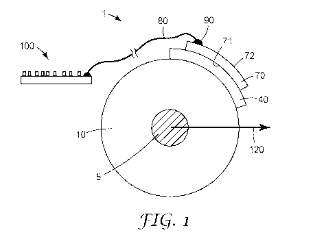
Figure 1 is a schematic cross section of a first conductor assembly 1
according to the invention
and a circuit board. An insulating layer 10 is arranged concentrically on an
inner conductor 5 of
circular cross section. The inner conductor 5 and the insulating layer 10 are
an inner conductor
and an insulating layer of a high-voltage power cable. The conductor 5 extends
longitudinally
perpendicular to the plane of the drawing, defining radial and axial
directions. A radial direction
120, pointing away from the center of the inner conductor 5, is indicated by
arrow 120, axial
directions are perpendicular to the plane of the drawing.
A sensing electrode 40 is arranged radially outward of the insulating layer
10, and on the
insulating layer 10. The sensing electrode 40 is electrically conductive and
comprises a piece of
electrically conductive metal foil. The sensing electrode 40 extends, in cross
section, around a
part of the circumference of the insulating layer 10, namely around about a
fifth of the
8
CA 02915392 2015-12-14
WO 2014/205170
PCT/US2014/043103
circumference. The sensing electrode 40 is attached to the insulating layer 10
adhesively. The
sensing electrode 40 and the inner conductor 5 are operable as electrodes of a
sensing
capacitor, with the insulating layer 10, arranged between the electrodes,
being operable as a
dielectric of the sensing capacitor. The sensing capacitor, in turn, is
electrically connected such
as to be operable as a first dividing capacitor in a capacitive voltage
divider. The capacitive
voltage divider comprises a second dividing capacitor (not shown), which is
electrically
connected with the first dividing capacitor and with electrical ground. The
capacitive voltage
divider is part of a sensor for sensing a voltage of the inner conductor 5
relative to electrical
ground.
The inner conductor 5 and the insulating layer 10 are comprised in a high-
voltage power cable.
That cable comprises further layers at an axial distance from the area where
the cross section
of Figure 1 is taken: the cable comprises a semiconductive layer arranged on
the insulating
layer 10, a shielding layer arranged on the semiconductive layer, and a cable
sheath arranged
around the shielding layer. In the axial section where the sensing electrode
40 is arranged on
the insulating layer 10, the outer layers of the cable have been removed such
as to expose the
insulating layer 10. The sensing electrode 40 is applied on the insulating
layer 10 in the stripped
section of the cable.
The conductor assembly 1 further comprises a voltage pickup element 70. The
voltage pickup
element 70 has a first major surface 71 and an opposed second major surface
72. The voltage
pickup element 70 is an electrically conductive polymer film. Because the
polymer film is in itself
electrically conductive, the major surfaces 71, 72 of the voltage pickup
element 70 are
conductive, too. The first major surface 71 is arranged on the radially outer
major surface of the
sensing electrode 40. The first major surface 71 of the voltage pickup element
70 is therefore in
a surface contact with the sensing electrode 40. The sensing electrode 40 and
the first major
surface 71 of the voltage pickup element 70 are electrically connected and on
the same
electrical potential. It can thus be said that the voltage pickup element 70
picks up the voltage of
the sensing electrode 40. Due to the extended contact area between these
elements, resistive
losses between the sensing electrode 40 and the voltage pickup element 70 are
reduced. The
voltage pickup element 70 extends around a smaller portion of the
circumference of the
insulating layer 10 than the sensing electrode 40 extends, in cross section.
An electrically conductive electrode wire 80 is attached to the voltage pickup
element 70 at a
contact point 90 on the second major surface 72. Its end portion is soldered
to the contact point
9
CA 02915392 2015-12-14
WO 2014/205170
PCT/US2014/043103
90, so that the electrode wire 80 is in electrical and mechanical contact with
the voltage pickup
element 70. The contact point 90 is electrically conductive and electrically
connects the voltage
pickup element 70 and the electrode wire 80 with each other. Thereby, the
electrode wire 80,
the contact point 90, the voltage pickup element 70 and the sensing electrode
40 are electrically
connected with each other.
The electrode wire 80 extends from the contact point 90 to a circuit board
100. An end portion of
the electrode wire 80 is attached to the circuit board 100. On the circuit
board 100, the electrode
wire 80 is electrically connected to a further capacitor. This further
capacitor is the second
/0 dividing capacitor of a capacitive voltage divider. The capacitive
voltage divider allows sensing
the voltage of the inner conductor 5 relative to electrical ground. Electrical
circuits for this
voltage sensing are known. In addition to the further capacitor, other
electric or electronic
components for sensing the voltage of the inner conductor 5, are arranged on
the circuit board
100. The further capacitor and the other electric or electronic components
and/or the circuit
board 100 are arranged more than 10 millimetres away from the sensing
electrode 40, in other
words, they are arranged remote from the sensing electrode 40. The electrode
wire 80 makes
the voltage signal of the sensing electrode 40 available at a location remote
from the sensing
electrode 40.
Figure 2 is a schematic cross section of a second conductor assembly 1'
according to the
invention and a circuit board 100. The second conductor assembly 1' and the
circuit board 100
are identical to the first conductor assembly 1 and the circuit board 100
shown in Figure 1,
except that the sensing electrode 40' extends around the full circumference of
the insulating
layer 10, in cross section. Also in the second conductor assembly 1', the
inner conductor 5 and
the insulating layer 10 are an inner conductor and an insulating layer of a
high-voltage power
cable, respectively. The sensing electrode 40' is formed by a ring-shaped
portion of a
semiconductive layer of the cable, which is electrically isolated from other
portions of the
semiconductive layer of the cable. That semiconductive layer is a regular
layer of the cable. In
the stripped portion of the cable, shown in the cross section of Figure 2, the
semiconductive
layer has been removed such as to expose the insulating layer 10 of the cable,
except in an
axial section of the cable, where a ring-shaped axial section of the
semiconductive layer was left
on the insulating layer 10. This ring-shaped section forms the sensing
electrode 40 visible in
Figure 2. The remaining ring-shaped section is electrically isolated from the
other portions of the
semiconductive layer of the cable, that were not removed by stripping, so that
this ring-shaped
section can serve as a sensing electrode 40'.
CA 02915392 2015-12-14
WO 2014/205170
PCT/US2014/043103
The voltage pickup element 70 and the electrode wire 80 are identical to the
corresponding
elements in the conductor assembly shown in Figure 1. Again, the circuit board
100 is located
remote from the sensing electrode 40'.
Figure 3 is a further schematic cross section of a third conductor assembly 1"
according to the
invention. It is similar to the first conductor assembly 1, except for the
presence of a spacer
layer 25, which is arranged on the outer surface of the insulating layer 10
and thus between the
insulating layer 10 and the sensing electrode 40. The spacer layer 25 extends,
in the cross
section, around the full circumference of the insulating layer 10. Since a
portion the spacer layer
25 is arranged between the insulating layer 10 and the sensing electrode 40,
the spacer layer
25 is operable as a further dielectric of the sensing capacitor, which
comprises the inner
conductor 5 and the sensing electrode 40 as electrodes, and the insulating
layer 10 as a
dielectric. The spacer layer 25 establishes a certain distance between the
sensing electrode 40
and the inner conductor 5. By choosing a specific thickness and specific
electrical properties of
the spacer layer 25, the voltage signal on the sensing electrode 40 can be
adjusted, so that the
signal is in a certain voltage range for a given voltage of the inner
conductor.
Figure 4 is a further schematic cross section of a fourth conductor assembly
1¨ according to
the invention. It is similar to the first conductor assembly 1, except for the
voltage pickup
element 70' comprising a multilayer circuit board 240. The multilayer circuit
board 240 has a first
skin layer 230 and an opposed second skin layer 210. Both skin layers 210, 230
are electrically
conductive. The skin layers 210, 230 are the outermost layers of the
multilayer circuit board
240. The first skin layer 230 comprises the first major surface 71 of the
voltage pickup element
70'. The second skin layer 210 comprises the second major surface 72 of the
voltage pickup
element 70'. Between the skin layers 210, 230, an intermediate layer 220 is
arranged. The
intermediate layer 220 comprises a conductive via 225, which provides an
electrical connection
between the first skin layer 230 and the second skin layer 210. Thereby, the
first major surface
71 and the second major surface 72 of the voltage pickup element 70' are
electrically connected
with each other.
The intermediate layer 220 can accommodate electric or electronic components
227 for
processing the voltage signal picked up from the sensing electrode 40. It can
accommodate
conductive traces (not shown) for electrically connecting the skin layers 210,
230 and/or the
electric or electronic components with each other.
11
CA 02915392 2015-12-14
WO 2014/205170
PCT/US2014/043103
Figure 5 is a sketched perspective view of the first conductor assembly 1 and
the circuit board
100 of Figure 1. The conductor assembly 1 comprises a high-voltage power cable
2. The cable
2 comprises the insulating layer 10, concentrically arranged around the inner
conductor 5 (not
visible). The conductor 5 defines radial directions 120 and axial directions
indicated by a double
arrow 110. A semiconductive layer 20 is arranged concentrically around the
insulating layer 10,
and an electrically insulating cable sheath 30 is arranged around the
semiconductive layer 20 of
the cable 2. In an axial section, the cable 2 is stripped, i.e. the cable
sheath 30 and the
semiconductive layer 20 are removed, so that the insulating layer 10 is
exposed. In the stripped
section, the sensing electrode 40 is arranged on the insulating layer 10, and
the voltage pickup
element 70 is arranged on the sensing electrode 40, so that the sensing
electrode 40 is
arranged radially between the insulating layer 10 and the voltage pickup
element 70. The cross
section of Figure 1 is taken in the section of the cable 2 in which the
sensing electrode 40 and
the voltage pickup element 70 are arranged on the insulating layer 10.
The electrode wire 80 is attached to the voltage pickup element 70 at the
connection point 90.
The electrode wire 80 conducts the voltage signal of the sensing electrode 40
to the remotely
located circuit board 100, on which the second dividing capacitor (not shown)
of the capacitive
voltage divider is arranged, which is part of the voltage sensor for sensing
the voltage of the
inner conductor 5.
12