Note: Descriptions are shown in the official language in which they were submitted.
CA 02916038 2015-12-17
WO 2015/030952 PCT/US2014/047519
HEAT SINK COMPOSITION FOR ELECTRICALLY RESISTIVE AND
THERMALLY CONDUCTIVE CIRCUIT BREAKER AND LOAD CENTER
AND METHOD OF PREPARATION THEREFOR
CROSS-REFERENCE TO RELATED APPLICATION
This application claims priority from and claims the benefit U.S..
Patent Application .Serial No. PI/012,308, filed .August 28, 2.013, Skili Ch.
is
incorporated by referent* herein,
BAC=KGROUND
I 0 Field
The disclosed concept .pertains generally to electrical switching
apparatus and, more particularly, to circuit interrupters, such as eironn
breakers and
load panels or centers. The disclosed concept further pertains to compositions
for
manufacturing electrical switching apparatus and related enclosures, and
methods for
preparing the compositions.
Backaround Information
Electrical switching apparatus include,. for example, circuit switching
devices and circuit interrupters, such as circuit breakers, contactors, motor
starters,
2.0 motor controllers and other load centers. These apparatus are generally
well known in
the art. :For example, circuit breakers are known to include at least one pair
of
separable contacts which are operated to protect electrical circuitry from
damage due,
to ari overcurrent con.dition, such as an overload condition or a relatively
high level
short circuit or fault condition. Electrical switching apparatus generally
include a
housing to provide an enclosure for the electronics contained therein, e.g.,
separable
contacts, operating mechanism and trip mechanism, as well as to provide
strength and
temperature insulation. The material of construction for the housing can be
selected
from. a -V:U.10y of known matOriats.-Which may be. molded in various
geometries, such
as but not- limited -to liquid crystal polymer -thermoplastic,. In some
instances, the
housing can be formed by a process known as insert molding which is an
injection
molding process whereby resin is introduced, injected, into a cavity or
mold and
then allowed to set or cure.. The result is a single molded plastic piece,
e.g., housing,
- -
CA 02916038 2015-12-17
WO 2015/030952 PCT/US2014/047519
Typically, the -molded plastic used in an electrical switching apparatus,
e.g., circuit breaker or load center is .electrically reststiye,
cartent cannot
pass therethroughõ such as to provide a barrier to shield and protect
personnel located
outside of the apparatus from contact -with .electrically conductive parts,
and the
potential for electrocution.
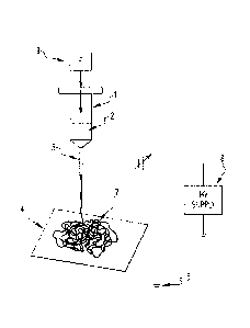
Aso known in the art are various techniques for producing composite
.fibers in nanoscale dimensions, such as dectrospinning and ForceSpinningTM
technology, A typical electrospinning process is illustrated in FIG, 1. As
shown 111
FIG. 1, the electrospinning apparatus includes a syringe 1 containing a
polymer
molten mass 2 or a sohltiOn. A spinning capillary 3 is located at the tip of
the syringe
I, which is coupled with a pole of tbe voltage-generating arrangement, 6
(current
supply.). By means of an injection pump 9, the polymer molten mass -2 is
transported
out of the syringe I towards the spinning capillary 3., where drops are.
tbrined at the
tip, The surface tension of the drop of the polymer molten mass 2 or solution
coming
out .of the spinning capillary 3 is OVerCOIlle by means of an electric field
between the
spinning capillary 3 and a counter electrode 5. Then, the drop coming out of -
the
spinning capillary-3 deforms and when it reaches a critical. electric
potential it is.
drawn to yield. a fine filament, the so-called jet. This electrically-charged
jet,
continuously extracting new polymer molten mass 2 Or SO1116011 from the
spinning
capillary 3 is then accelerated in the electric field towards the counter
electrode 5..
The jet solidifies .during its flight towards the counter electrode 5 tiy
means of the
evaporation of the solvent- or by -means of cooling,. such that in a short
period of time
continuous nanofibers 7 are generated, linked with one another, witiì typical
diaineters.
.of a few nanometers to .several micrometers. These nano-fibers 7 are
deposited on the
template 4 associated with the counter electrode. 5 in the fonn of a web or
TIODWOVen
mat. The conductive template 4 serves as a collector and is grounded together
With
the counter electrode 5. The polymer nanotibers 7 are spun directly on the
conductive
template: 4-,
A typical ForceSpinnine apparatus. (which is commercially available
.from FibeRie Technology Corporation) is illustrated in FIG, 2. As shown in
FIG. 2,
the ForeeSpinningim- apparatus includes a. spinneret 20 having a reservoir 22
.containing a liquid state material 24. :During operation, the spinneret 20 is
rotated
- 2 -
CA 02916038 2015-12-17
WO 2015/030952
PCT/US2014/047519
centrifiwally on an axis:.25 at high revolutions per minutecreating
hydrostatic and.
centrifugal forces_ As the spinneret 20 rotates, the hydrostatic and
centrifugal .forOes
push the liquid state material 24 to an outer wall 26 having an orifice 27
located
therein. FIG. 2 shows .one orifice 27; however, it is contemplated that a
plurality of
orifices may be formed in the outer wall 2.6. The liquid state material 24
enters the
one or more orifices 27 and is released. therefrom_ The centrifugal and
hydrostatic
.forces combine to initiate a jet of the liquid state material 24 that
impinges against a
fiber collector 28 to produce nanolibers 29. In FIG. 2, the fiber collector 28
is
positioned to surround only a. portion of the spinneret 20; however, it is
contemplated
that the fiber collector 28 may be positioned to surround up to the entire
circumference of the spinneret 2Ø
The electrostatic force used to create nanofibers in an electrospirming
apparatus is replaced by .centrifugal forces in the FotteSpinnine.apparatus.
The
liquid state .material can include solutions or molten materials, such as
polymer melt.
Examples of suitable materials include thermoplasticõ thermoset resins and
ranì.
extruded polymers, such as polytetralinoroethylene (VIM). In addition to
nanofibers, the apparatus can also produce libels in the micron or submicron
range.
In th.e ForceSpinninglm technology, conductivity and/or electrostatic charge
are not
relevant parameters for the selection of materials to create the fibers and
thus., the
spectrum of materials to be spun may be broader as compared with
electrospinning,
e.g.., materials with low dielectric constants can be spun into nanofibers
without the
.additional of salt or solvent. The controlled .variables for .the
ForceSpinning"
apparatus are rotational speed of the spinneret, design of the collection
system and,
and shape and size of the orifice&
It is also .known in the art -to produce injeCtion molded parts by
injecting a polymer material into a mold. In a typical injection molding
manufacturing process, heated molten plastic is forced into a mold cavity
under
pressore. Injection molding .consists of a die containing a mold cavity which
is
.formed to the shape of the desired finished component and is in direct fluid.
communication with a source of molten material, e4.14.., typically resin but
can also
include metal. The Molten material is forced into the mold cavity and allowed
to cool
and set. As a result:, the molten .material conforms to the shape of the
cavity. Th.e
- 3 -
CA 02916038 2015-12-17
WO 2015/030952 PCT/US2014/047519
cooled component is then removed from the mold cavity. This process. then can
be
repeated to produce additional components.
In general, a. mold cavity is a negative part being produced. That is,
when the. cavity is filled WitSIi plastic, it is cooled and the plastic
becomes solid
material resulting in a completed positive component.
Injection pressures Carl vary and can be in a range from 5,000 to
20õ000 psi. Due to th.e high pressures involved, molds ..may need to be
clamped shut
dully, injection and cooling -using clamping forces measured in tons..
Conventional injection .molding techniques are capable of producing a
large number of components with high levels of precision and consistency. For
exitinple, holding tolerances of less than 0,00.1 inch (.0025 nun) can be
relatively
easily accomplished with the appropriate.com.bination of material,. component
design
and .mold. design. It has been demonstrated that even .narrower (i.e.,õ
tighter)
tolerances can be .achieved with additional effort.
Conventional processes for the m.anufacture of electrical switching
apparatus, e.g., circuit breakers, and .enclosures typically utilize molding
materials
that are thermal insulators. in general., thermal insulators provide for low
or illirthITUITI
thermal conduction and heat dissipation. Thus, the. circuit 'breakers arid
enclosures
manufactured from therm.al insulators electrically and thermally insulate the
electronics contained therein from the current .carrying operating mechanism.
As a.
result, the terminals or other critical locations of the circuit breakers and
enclosures
may have elevated temperatures. It is known in -the art to measure and record
these
temperatures (in the terminals or other critical locations) to assure safe
operation and.
limited degradation or failure.
Accordingly, there is mom for improvement in identifying materials
for construction of molded electrical switching apparatus. It is desired to
provide
molding compositions Nvhich are electrically resistive and more thermally'
conductive
for use in manufacturing electrical switching a.pparatus and ..enclosures, and
.ultimately
to allow these apparatus to dissipate heat therebyteducing the amount of heat
transferred and. decreasing the temperature of the terminals or other critical
'locations,
- 4 -
CA 02916038 2015-12-17
WO 2015/030952 PCT/US2014/047519
Further, there is .room for .improvement in producing injection inolded
parts and,. in particular, functionalizing the molded part in order to impart
selected
properties: thereto.
SUNIMA.RY
'These needs and others are .met by embodiments of the disclosed
concept
In accordance -with .one aspect of the disclosed concept, there is
provided a composition for the manufacture of an electrically resistive and
thermally
conductive electrical switching apparatus. The composition includes a first
component including polymer and a second component including nanofibers. The
thermal conductivity of the second component is higher than the thermal
conductivity.
of the first cOMpOnent such that the electrical switching apparatus including
the
composition has improved heat dissipation as compared to an electrical
switching
apparatus constructed of the first component in the absence of the second
component.
I 5 The second component includes fiber material selected .from
polymer,
polymer-containing material, metal, metal-containing material, inorganic
material,
and mixtures thereof and .filler. The filler can have higher thermal
conductivity than.
the thermal conductivity of each of the fiber material and the first
component.
In certain embodiments, the first and second components can be
combined to form a mixture. The mixture can be subjected to an injection
molding
process to form a molded object which forms at least a portion of the
electrical
switching apparatus.
in certain other embodiments, the.first component can le subjected to
an injection molding process to form a molded object .Which forms at least a
portion
of the electrical switching apparatus and the second component can be
deposited on at
least a portion of an outer surface .of the molded object. The second
component can.
be in the form of a mat. The mat can be porous and furthermore, the molded
object
having the second component .deposited on the .outer surface can be
transparent.
In accordance with another aspect .of the disclosed concept, there..is
provided a. method of preparing a molded component for manufacturing an
electrically resistive and thermally conductive electrical switching
apparatus. The
meth.od includes obtaining a first component comprising polymer and obtaining
a
5 -
CA 02916038 2015-12-17
WO 2015/030952 PCT/US2014/047519
second component The second component includes fiber .material selected from
poi ynia,. poly.mer-containing .material, metal, metal-containing material,
inorg.anic
material., and, mixtures thereof; and, filler,. The thermal conductivity of
the second
component is higher than thermal conductivity of the first component such that
the
electrical switching apparatus comprising the molded component has improved
heat
dissipation as compared to an .electrical switching apparatus comprising the
first
component in absence of the second component, The .method further includes
combining the first component and the second component in an injection molding
process to form a molded component, wherein the molded component at least
partially forins the electrical switching apparatus.
The second component can include a layer of nanofibers at least
partially deposited on a carrier substrate,
In certain embodiments., the combining of the first and second
components can include at least partially depositing the second component on
an
inner surface of the mold, introducing the first component into the mold,
allowing the
first .component to set, transferring at least partially the second component
from the
inner surface of the mold to an outer surface of the molded component and
extracting
the ..molded component from the mold. hi these embodiments, the second
component
can include nanofibers deposited on a carrier film. Alternatively, the second
component can include nanofibers deposited directly .on the inner surface of
the mold
in the absence of a miler film.
In accordance with yet another aspect of the disclosed concept there is
provided a method of lowering the :internal temperature of an electrically
resistive and.
thermally conductive :electrical switching apparatus. The method includes
preparing a
material of construction of the electrical switching apparatus by combining a
first
component including polymer and a second component including nanolthers to
form a
mixture. The thermal conductivity of the second component is higher than the.
thermal .conductiYity of the first component such that the electrical_
switching
apparatus .including the mixture has improved 'heat .dissipation :as compared
to an
eleorical switching apparatus constructed of the first component in the
absence of the
second component. The mixture is poured into a mold and allowed to set. The
set
- 6 -
CA 02916038 2015-12-17
WO 2015/030952
PCT/US2014/047519
mixture is then extracted: from the ntold to forin a molded part which is used
to form
at least a portion of the electrical switching apparatus.
BRIEF DESCRIPTION OF THE DRAWINGS.
A full understanding of the disclosed concept can be gained from the
following .description of the preferred embodiments when read in conitmotion
with the
accompanying drawings in which:
FIG. I is schematic of a conventional .electrospinning apparatus, in
accordance with the prior art.
FICi. 2 is a schematic of a typical ForceSpinningrm apparatus, in
accordance with the prior art.
FIGs. 3.A, B and C are schematics of a process for depositing
nanofibers into a mold and subsequently onto a molded part, in accordance with
certain embodiments of the disclosed concept.
DESCRIPTION OF THE PREF:ERRED EMBODIMENTS
As employed herein, the term "load center" shall mean a. load panel, a
panelboardõ a circuit breaker panel, or any. suitable enclosure .enclosing or
housing a
plurality of circuit breakers for a plurality of branch or other load
circuits. Further, as
employed herein, the term. "electrical switching apparatus" shall encompass
related
enclosures or housinsts.
As employed herein, the statement that, two or more parts are.
"connected" together shall mean that the parts are joined together either
directly- or
joined -through one or .more intermediate parts. Furtherõ as employed herein,
the
statement that 0,vo or more parts. are "attached" shall mean that. the parts
are joined
together directly,
The disclosed concept is described in association with electrical
switching apparatus., such as circuit breakers and loa.d centers, and related
enclosures,
although it will become apparent that it could also be applied to other types
of
electrical switching apparatus (e.g.. .without limitatiOriõ other .circuit
switching devices
and other circuit interrupters such as contactors, motor starters., motor
.controllers and.
other load controllers).
.In certain embodiments., the disclosed concept includes an electrically
resistive, heat sink compositions for making at least a portion of
electrically resistive,
- 7 -
CA 02916038 2015-12-17
WO 2015/030952 PCT/US2014/047519
thermally conductive electrical switching apparatus, such as circuit breakers
and.
enclosures. It is knosvn in the art to. construct electrical's-witching
apparatus from
electrically resistive materials. Further, it is known in the art to construct
electrical
switching; apparatus from thertnal insulating; materials, such. as pol.ymer,
including; but
not limited to liquid crystal polymer. Polymers are not highly thermally
conductive
materials and therefore, are not very effective to dissipate heat. As a.
result, the.
conventional electrical switching apparatus, such as circuit breakers and
enclosures
that are .formed from polymer, retain heat and therefore, result in an
elevated.
temperature. Current operating practices can include measuring and recording
temperatures in an area surrounding circuit breakers or nearby to monitor and
control
temperature increases.
There are various materials that are known to be stitable thermal_
conductors.. However, these known materials typically are also electrically
conductive. Due to critical safety considerations, a material for use in
manufacturing
electrical switching apparatus must exhibit electrical insulating properties.
Thus, a
suitable material of construction for electrical switching apparatus cannot
merely
exhibit thermal eonductivity.properties in the absence of electrical resistive
properties,
A. desirable material for use in manufacturing, electrical switching apparatus
shall
demonstrate .electrical resistive properties in conjunction with thermal
conductivity
properties. An advantage of the disclosed concept is that a molded composition
can
be formed to manufacttue electrical switching apparatus that exhibit both
electrical
resistive and thermal .conductivity properties, such that the apparatus is
.capable of
dissipating heat (without becoming an electrical .conductot),
in the disclosed concept, electrically resistive;.thermally conductive
electrical switching apparatus are manufactured .from a composition containing
a first
component including polymer and a second component including nanolibers. The
nanofibers exhibit a higher thermal condu.etivity than the polymer component
and
therefore, the presence of the nanofiber component in the composition is
effective to
.increase the thermal conductivity of an electrical switching a.pparatus
!brined from the
composition. 'Thus, for example, in circuit breakers .fonned from the
composition of
the disclosed concept, the presence of the nanofiber component is effective to
increase
the dissipation of heat by the circuit breaker and thereby .reduce the amount
of heat
- 8 -
CA 02916038 2015-12-17
WO 2015/030952 PCT/US2014/047519
transferred from the circuit breaker to the terminals or other locations
(where
temperattire increases typically need to be ITIonitored and comfolled).
In certain embodiments., the composition of the disclosed concept can
be utilized to form a back pan of an enclosure to increase the thermal
conductivity of
this area, decrease the internal temperature of the enclosure, and dissipate
heat to a
load center. The load center is typically constructed of metal, such as steel,
and
therefore, even though the temperature of the load center may increase (e.g.,
it may
feel warm to the touch) as the result of heat transferred from the enclosure,
the metal
construction of the load center Axil] provide for heat dissipation.
The nanofibers of the composition are prepared using fiber material
and filler. The fiber material includes polymer, polymer-containing material,
metal,
metalacontaining material, inorganic material, such as .ceramic, and mixtures
thereof.
Suitable fdlers fOr use can be selected from a Nvide \quiet)" of known
materials. in
general, different fillers can exhibit ditTerent properties and can impart
these different
properties w the polymer .component and the .composition, and ultimately an
electrical
switching apparatus which is at least partially constructed of the
composition.
Specific filler is selected based on its material properties functionality and
therefore,
the property or functionality that is desired .for the resulting composition
or .molded
part, e.g., electrical switching apparatus. For .example, a thermally
conductive filler is
used to prepare .nanofibers which are combined tivith a polymer component to
impart
thermal conductivity to the polymer component (which is not highly thermal
conductive) and ultimately to the resulting .electrical switching apparatus
constructed
therefrom. The filler (and the: restating nanofiber component) ex.hibits
higher thermal
conductivitylhan the polymer-component, such that the .thermal conductivity of
the.
composition of the disclosed. concept is higher than the thermal conductivity
ofthe
polymer cotnponent.
The nanofiber component can be prepared utilizing various
conventional .techniques known in the art .including, but not limited to,
electrospinning
and. ForceSpinning. Electrospinning techniques can be conducted at .ambient
temperature and pressure conditions. ForceSpinning is typically conducted at
elevated temperature conditions., e.g.õ the melt temperature of the fiber
material used
to .form the nanofibers.
CA 02916038 2015-12-17
WO 2015/030952 PCT/US2014/047519
The polymer component .includes polymer andlor polymer-containing
material., e., matrix., and can be. selected from thosematerials known for
manufacturing electrical switching apparatus.
The polymer .component and nanofiber component are .combined to
form the electrically -resistive, heat sink composition for making
electrically resistive,
thermally conductive electrical switching, apparatus, such as circuit
'breakers and
enclosures, in accordance -with the disclosed concept. The nanofiber component
can
be prepared and then incorporated into the fast polymer component. For
example, the
polymer component can be used to form a molded object, e.g., the electrical
switching
apparatus or a portion thereof utilizing a conventional injection molding
technique.
:in general, injection molding involves selecting a cavity or mold, at least
partially
filling, injecting) the. cavity or m.old ivith a material, .e.g., the
polymer
component, allowing .the filled cavity .or mold to set or cure, and extracting
the
molded object therefrom. The molded object can be formed at ambient
temperature
and pressure conditions.
In certain embodiments:, the nanofiber component is incorporated into
the polymer .component by at least partially enibedding nanofibers in or
depositing
nanofibers on an Outer:surface of the molded object. As :previously described,
the
nanofiber component is prepared using a conventional technique known in the
art
For example, electrospinning .or Force:Spinning can be employed to form and
deposit
nanofibers on a substrate or collector. in alternate embodiments,. a layer of
nanofibers
can be a.t least partially formed on a collector, e.g..õ a carrier film, and
then the
collector having the layer ofnanofibers can be applied to a substrate, or a.
layer of
nanofibers can be formed directly on the substrate., e.gõ directly on an inner
surface of
a mold, in the absence of a carrier film, In the embodiments wherein the
nanofibers
are formed on a carrier film, the carrier film is .applied, e.g., connected or
attached, to
an inner surf-lice of a cavity or mold such that upon filling of the cavity or
mold, the
polymer component comt..!$ into .contact with the nanofibers on the film and
upon.
extracting the .molded polymer component from the .mold, the nanofibers.:are
at. least
partially transferred .from the surface of the film to an outer surface of the
molded
polymer component, such that the nanofibers are at least partially embedded in
(e.g.,
inftised) or deposited on (e.g., coated on or layered on or laminated on) the
outer
CA 02916038 2015-12-17
WO 2015/030952 PCT/US2014/047519
SurffiCe to .fbrat a molded part Or component including each of the polymer
and
nanofiber components. The carrier fihm. is not transferred and remains at
least
partially in the mold or on the inner surface of the mold.
Alternatively, in the embodiments, wherein the nanofibers are formed
directly on at least a portion of the inner surface of the mold, upon filling
of the cavity
or .mold, the polymer component comes into contact \via" the nanofibers on the
inner
surface of the mold and upon .extracting the molded polymer component from the
mold, the nanofibers are at least partially transferred from the inner surface
of the
mold to an outer surface of the .molded polymer component, such that the
nanofibers
are at least partially embedded in tes..õ infused) or deposited on (e.g.,
coated on or
layered on or laminated on the outer surface to form a molded composition
including
eaCh of the polymer and nanofiber components.
The nanofiber component can be in the forin of a web or mat, es.,
non-woven. The web or mat can be highly porous, in certain embodiments.
wherein
the polymer .component is optically transparent, deposition of the nanofiber
component on the surface of the molded. poly-fuer .component does not
significantly
decrease the optical transparency of the resulting molded composition.
The diameter of the nanofibers can vary and in certain embodiments,.
Call be from about 10 nanometers to about 10 microns,. 'Without intending to
be bound
by any particular theory, it is believed that the use of fibers whicIli are of
a nanoscale
size results in improved interaction and bonding between the nanofiber
component
and the polymer .component.
111 certain embodiments, the surface conductivity of the molded
composition including the polymer component and the nanofiber component is
from
about l 0 ohms to about 100 mega-ohms. The surface conductivity of the
..molded
composition can be controlled and tailored by the particular filler selected
and the
specific amount of filler.
HG. 3 illustrates an apparatus and process.for depositing a:toating of
nanofibers on at least a portion of a surfaceof a molded part, .accordance
.with
certain embodiments of the disclosed concept. As shown in FIG, 3A, a foil
positioning step is em.ployed to initiate the process. The apparatus for this
step
includes a die 30, a carrier .film 3.2 and conducting .nanofibers 34, The
conducting
l
CA 02916038 2015-12-17
WO 2015/030952 PCT/US2014/047519
nanofihers 34 are deposited onto the carrier film 32 and form a. lay.er
thereon. A
nozzle 36 having a nozzle head 38 is used to inject material 39 into the die
3Q. Thus,
the nozzle 36 includes the nozzle head 38 and the material $9 contained
therein,. The
material 39 can include polymer or pollyMer-containing material, such as
resin. FICi,
3B further shows an injection molding- step which includes the carrier film 32
containing, the conducting nanofibers 34 in .contact with, .e.g.õ attached or
applied to,.
an interior surface of the die 30. Th.e nozzle head 38 injects the material 39
into the
die 30. FIG. 3C ShOWS an extraction step wherein a .molded part 40 is produced
and
an outer surface of the molded part 40 has deposited therein or thereon the
conducting
nanofibers 34 which are at least partially transferred from the carrier film
32 which is
remaining on the interior surface of tbe die 30 The presence of the conducting
nanofibers 34 on or in the Stithee of the molded part 40 allows the surface
conductivity.of the m.olded. part 40 to be controlled or specified.
Each of the polymer and nanofiber components of the disclosed.
concept can include additional additives and adjuvants which are known in the
art for
use in preparing polymer-containing compositions and molded objects.
In certain embodiments, at least a portion of an electrically resistive,
thermally conductive electrical switching apparatus is formed from the
composition of
the disclosed concept by combining the polymer and naaofiber components., and
any
additional additives to fonn a mixture. The mixture is then poured or injected
into a
cavity or mold and allowed to set or cure for an appropriate period of =time
to form a
single molded piece:, e.g, electrical switching apparatus, including the
polymer
component and the nanofiber coruponent incorporated therein.
The composition of the disclosed:concept may serve as a 'heat sink in
an electrically resistive electrical switching apparatus, such as but not
limited to a
circuit breaker, an enclosure and a load center.
While specific embodiments of the disclosed concept have been
described in detail, ít will be appreciated by those skilled in the art that
VadOUS
modifications and alternatives. to those detaits could be developed in light
of the
$0 overall teachings of the disclosure. Accordingly, the particular
.arrangements
disclosed are meant to be illustrative .only and not limiting as to the scope
of the
- 12 -
CA 02916038 2015-12-17
WO 2015/030952
PCT/US2014/047519
disclosed concept which is to be given the .full breadth of the claims
appended and.
any and all equivalents thereof.