Note: Descriptions are shown in the official language in which they were submitted.
CA 02916321 2015-12-29
Time-Coherent Global Network
CROSS-REFERENCE TO RELATED APPLICATIONS
The present application is a division of application CA 2676868.
FIELD OF THE INVENTION
The present invention relates to high-capacity networks employing fast-
switching
bufferless core nodes.
BACKGROUND
Present wide-coverage data networks are generally multi-hop networks of large
diameter where a path from one edge node to another may traverse several
intermediate nodes. Such networks employ routers of moderate dimensions and
have
performance challenges. A multi-hop packet-switching network suffers from
cumulative
performance degradation as a path from source to destination traverses
numerous
routing nodes. It is well known that structural simplicity reduces network
cost and
improves its performance. In order to facilitate the introduction of high-
quality broadband
services, the network structure need be simplified and the network diameter
need be
reduced. It is desirable that a path from one edge node to another traverse a
small
number of intermediate nodes. It is also desirable, given the dominance of
fiber-optic
transport, that modulated optical carrier signals received at a core node be
switched
towards its destination edge node without the need for extracting the baseband
signals
for switching in the electronic domain.
There is a need, therefore, for a high-capacity network of small diameter that
employs fast-switching optical core nodes, and it may be argued that it is
more efficient
to create an entirely new global broadband network of high quality and
relatively low
cost.
1
CA 02916321 2015-12-29
SUMMARY
In accordance with one aspect, the present invention provides a network
comprising a plurality of switch units and a plurality of edge nodes. The
switch units are
arranged in a matrix having v columns and v rows, v>1. Each switch unit has n
inlet
ports and n outlet ports, n>1. Each edge node has v input ports, v output
ports, a
number of ingress ports, and a number of egress ports. The ingress ports
receive data
from data sources, and the egress ports transmit data to data sinks. Each
output port
has an upstream channel to a switch unit and each input port has a downstream
channel from a switch unit. The v output ports connect to v switch units in v
different
columns and the v input ports connect to switch units in v different rows.
Each switch unit has a switch-unit controller and a master time indicator.
Each
edge node has an edge controller and v slave time indicators each slave time
indicator
associated with a respective one of the v output ports. An edge controller of
an edge
node exchanges timing signals with each of the v switch units to which the
edge node
has an upstream channel in order to time-lock each of the v slave time
indicators to a
master time indicator of a respective switch unit.
In accordance with another aspect, the present invention provides a network
comprising a plurality of edge nodes, a plurality of switch units, a plurality
of upstream
wavelength routers, and a plurality of downstream wavelength routers.
The switch units are arranged in a matrix having v columns and v rows, v>1.
Each upstream wavelength router connects a respective first set of wavelength-
division-
multiplexed links originating from a respective subset of the edge nodes to a
respective
second set of wavelength-division-multiplexed links terminating in a
respective subset of
the switch units. Each downstream wavelength router connects a respective
third set of
wavelength-division-multiplexed links originating from a respective subset of
the switch
units to a respective fourth set of wavelength-division-multiplexed links
terminating in a
respective subset of the edge nodes.
2
CA 02916321 2015-12-29
The upstream wavelength routers collectively connect each edge node to a
respective set of v switch units, one in each of the v columns. The downstream
wavelength routers collectively connect each edge node to a respective group
of v
switch units, one in each of the v rows. Preferably, the group of switch units
belongs to
a single column in the matrix.
The upstream wavelength routers are configured so that each wavelength-
division-multiplexed link in the second set of wavelength-division-multiplexed
links
carries a wavelength channel from each wavelength-division-multiplexed link in
the first
set of wavelength-division-multiplexed links. The downstream wavelength
routers are
configured so that each wavelength-division-multiplexed link in the fourth set
of
wavelength-division-multiplexed links carries a wavelength channel from each
wavelength-division-multiplexed link in the third set of wavelength-division-
multiplexed
links.
Each edge node comprises an edge controller and each switch unit comprises a
switch-unit controller. Each switch unit has n inlet ports and n outlet ports,
n>1. The
switch units may comprise fast optical switches or single-rotator latent space
switches.
Each edge node time locks to respective v switch units to which the edge node
connects in the upstream direction. The plurality of edge nodes comprises at
most vxn
edge nodes. For global coverage, the value of v is preferably of the order of
1024 and
the value of n is of the order of 64, leading to a network supporting some
65000 edge
nodes.
In accordance with a further aspect, the present invention provides a network
comprising a plurality of edge nodes, a first plurality of switch units
arranged in a first
matrix, and a second plurality of switch units arranged in a second matrix.
The first
matrix has columns and pi rows, and each switch unit in the first matrix has m
inlet
ports and m outlet ports, p.>1, and m>1. The second matrix has v columns and v
rows,
and each switch unit in the second matrix has n inlet ports and n outlet
ports, v>1, and
3
CA 02916321 2015-12-29
n>1. The dimensions ju, m, v, and n are selected so that vxn=vxm. Thus, the
plurality of
edge nodes comprises at most vxn edge nodes.
Each edge node has IA upstream channels top, switch units belonging to ju
different columns of the first matrix and v upstream channels to v switch
units belonging
to v different columns of the second matrix. Each edge node has IA downstream
channels from a group of pi switch units belonging to ju different rows of the
first matrix
and v downstream channels from a group of v switch units belong to v different
rows of
the second matrix. Preferably, the group of IA switch units belongs to a
single column in
the first matrix, and the group of v switch units belongs to a single column
in the second
matrix. Preferably, a switch unit in the first matrix is configured as a
single-rotator latent
space switch, and a switch unit in the second matrix is configured as a fast
optical
switch. An edge node may be configured as a single-rotator circulating switch.
The network further comprises a plurality of upstream wavelength routers and a
plurality of downstream wavelength routers.
Each upstream wavelength router connects a respective first set of wavelength-
division-multiplexed links originating from a subset of the edge nodes to a
respective
second set of wavelength-division-multiplexed links terminating in a
respective subset of
the switch units selected from among the first plurality of switch units and
the second
plurality of switch units so that each edge node has p. upstream channels to
switch
units belonging to p, different columns of the first matrix and upstream
channels to p,
switch units belonging to p, different columns of the second matrix.
Each downstream wavelength router connects a respective third set of
wavelength-division-multiplexed links originating from a subset of the switch
units,
selected from among the first plurality of switch units and the second
plurality of switch
units, to a respective fourth set of wavelength-division-multiplexed links
terminating in a
respective subset of the edge nodes so that each edge node has p, downstream
channels from a group of [I switch units belonging to v different rows of the
first matrix,
4
CA 02916321 2015-12-29
and downstream channels from a group of VI, switch units belong to
different rows of
the second matrix.
An edge node has outbound ports connecting to switch units of the first matrix
and V outbound ports connecting to switch units of the second matrix. The edge
node
time locks each outbound port to a switch unit to which the outbound port
connects
through an upstream channel.
Preferably, the value of v is of the order of 1024, the value of p. is of the
order of
64, the value of n is of the order of 64, and the value of m is of the order
of 1024,
leading to a network supporting a number of edge nodes of the order of 65000,
which is
sufficient for global coverage.
In accordance with a further aspect, the present invention provides a uniphase
single-rotator circulating switch. The switch comprises N switch elements and
a single
rotator having N inlets and N outlets, N>2. Inlet j of the rotator connects to
outlet {j +
t}modul0 N during a time slot t of a time frame organized into N time slots,
0A<N.
The N switch elements are indexed as switch elements 0 to (N-1), the N inlets
are indexed as inlets 0 to (N-1), and the N outlets are indexed as outlets 0
to (N-1).
Each inlet connects to a 2:1 receiving selector and each outlet connects to a
1:2
sending selector.
A switch element comprises two internal output ports, two internal input
ports, an
external input port for receiving data from external data sources, and an
external output
port for transmitting data to external data sinks. The two internal output
ports of a switch
element of index k, (Xlc<N, alternately connect to inlet k of the single
rotator through a
respective 2:1 receiving selector during each time slot of the time frame, and
the two
internal input ports alternately connect to outlet {1--k}modulo N, (:W_<N, of
the single rotator
through a respective 1:2 sending selector during each time slot of the time
frame.
5
CA 02916321 2015-12-29
The single-rotator circulating switch further comprises an edge controller and
N
element controllers each element controller coupled to a respective one of the
N switch
elements. A temporal multiplexer time-multiplexes control signals sent from
the N
element controllers to the edge controller and a temporal demultiplexer
distributes
control signals sent from the edge controller to the N element controllers.
In accordance with a further aspect, the present invention provides a two-
phase
single-rotator circulating switch. The switch comprises N switch elements and
a single
rotator having N rotator inlets and N rotator outlets, N>2. Rotator inlet p of
the rotator
connects to rotator outlet {p + qmodulo N during a time slot t of a time frame
organized into
N time slots, aqp<N. Each rotator outlet alternately switches between two
respective
outlet ports during each time slot of the time frame and each rotator inlet
alternately
switches between two respective inlet ports during each time slot of a time
frame
organized into N time slots.
The N switch elements are indexed as switch elements 0 to (N-1), the N inlets
are indexed as inlets 0 to (N-1), and the N outlets are indexed as outlets 0
to (N-1).
A switch element comprises two internal input ports, two internal output
ports, an
external input port for receiving data from external data sources, and an
external output
port for transmitting data to external data sinks. The two internal output
ports alternately
connect to an inlet port of rotator inlet j and an inlet port of rotator inlet
{1---ilmodulo Al)
0.1_<N. The two internal input ports of a switch element of index j
alternately connect to
an outlet port of rotator outlet {L¨ilmoduio N, 0A<N, and an outlet port of
rotator outlet j.
The two-phase single-rotator circulating switch further comprises an edge
controller, for scheduling data transfer among the N switch elements, and N
element
controllers each element controller coupled to a respective one of the N
switch
elements. A temporal multiplexer time-multiplexes control signals sent from
the N
element controllers to the edge controller and a temporal demultiplexer
distributes
control signals sent from the edge controller to the N element controllers.
6
CA 02916321 2015-12-29
The two-phase single-rotator circulating switch provides two paths of
different
delays from a switch element j to a switch element k, Ol<N, 0_1<<N, H. Upon
receiving a request to establish a connection from switch element j to switch
element k,
the edge controller determines a value of ti¨klmodulo N and if the value is
less than the
integer part of (N+1)/2, the edge controller allocates paths for the
connection through
the internal port connecting to rotator inlet j. Otherwise, the edge
controller allocates
paths for the connection through the internal port connecting to rotator inlet
{L¨j}moduio N.
The two-phase single-rotator circulating switch further comprises an edge time
indicator coupled to the edge controller and N slave time indicators each
coupled to an
element controller of a switch element among the N switch elements.
The edge controller sends a first reading of the edge time indicator to an
external
controller of an external node communicatively coupled to a specific switch
element and
receives a corresponding second reading of a time indicator coupled to the
external
controller. The edge controller resets a slave time indicator of the specific
switch
element according to the first reading and the second reading.
In accordance with a further aspect, the present invention provides a two-
phase
single-rotator circulating switch. The switch comprises a single rotator
having N rotator
inlets and N rotator outlets, and (N-1) switch elements, N>2. Rotator inlet p
of the
rotator connects to rotator outlet {p + t}modulo N during a time slot t of a
time frame
organized into N time slots, 0.4<N. Each rotator outlet alternately switches
between two
respective outlet ports during each time slot of the time frame and each
rotator inlet
alternately switches between two respective inlet ports during each time slot
of a time
frame organized into N time slots.
The N inlets are indexed as inlets 0 to (N-1), the N outlets are indexed as
outlets
0 to (N-1), and the (N-1) switch elements are indexed as switch elements 0 to
(N-2).
A switch element comprises two internal input ports, two internal output
ports, an
external input port for receiving data from external data sources, and an
external output
7
CA 02916321 2015-12-29
port for transmitting data to external data sinks. The two internal output
ports alternately
connect to an inlet port of rotator inlet j and an inlet port of rotator inlet
{1--Dmodulo IV,
01._<N. The two internal input ports of a switch element of index j
alternately connect to
an outlet port of rotator outlet {1--llmodulo Ah 054<N, and an outlet port of
rotator outlet j.
An edge controller connects to an outlet port of rotator outlet 0, an outlet
port of
rotator outlet L, 0L<N, an inlet port of rotator inlet L, and an inlet port of
rotator inlet 0.
Each of the (N-1) switch elements has an element controller.
BRIEF DESCRIPTION OF THE DRAWINGS
Embodiments of the present invention will be further described with reference
to
the accompanying exemplary drawings, in which:
FIG. 1 illustrates a time-coherent network comprising edge nodes
interconnected
through independent switch units arranged in a matrix where each edge node has
upstream communication channels to switch units of a row and downstream
communication channels from switch units of a column, in accordance with an
embodiment of the present invention;
FIG. 2 further illustrates edge-node connections to switch units in the time-
coherent network of FIG. 1;
FIG. 3 illustrates a time-coherent network comprising edge nodes
interconnected
through independent switch units arranged in a matrix where each edge node has
upstream communication channels to switch units in different columns and
downstream
communication channels from switch units of a column, in accordance with an
embodiment of the present invention;
FIG. 4 illustrates a simple connection and a compound connection in the
network
of FIG. 3 in accordance with an embodiment of the present invention;
FIG. 5 illustrates a time-coherent network comprising edge nodes
interconnected
= through a network core comprising a first matrix of electronic switch
units, each switch
8
CA 02916321 2015-12-29
unit having a first number of dual inlet-outlet ports, and a second matrix of
photonic
switch units, each switch unit having a second number of dual inlet-outlet
ports, each
edge node having time-locked upstream channels to switch units of a row of the
first
matrix and time-locked upstream channels to a row of the second matrix where
the first
number is an integer multiple of the second number, in accordance with an
embodiment
of the present invention;
FIG. 6 illustrates downstream channels, in the network of FIG. 5, from switch
units of a column of the first matrix to an edge node and downstream channels
from a
column of the second matrix to the edge node, in accordance with an embodiment
of
the present invention;
FIG. 7 illustrates upstream channels from an edge node to switch units in
different rows and different columns of the two matrices of switch units of
the network of
FIG. 5, in accordance with an embodiment of the present invention;
FIG. 8 illustrates time-locked upstream channels from a set of edge nodes to
the
first matrix of switch units of the network of FIG. 5, in accordance with an
embodiment
of the present invention;
FIG. 9 illustrates time-locked upstream channels from a set of edge nodes to
the
second matrix of switch units of the network of FIG. 5, in accordance with an
embodiment of the present invention;
FIG. 10 illustrates downstream channels from the first matrix of switch units
of
the network of FIG. 5 to a set of edge nodes, in accordance with an embodiment
of the
present invention;
FIG. 11 illustrates downstream channels from the second matrix of switch units
of
the network of FIG. 5 to a set of edge nodes, in accordance with an embodiment
of the
present invention;
FIG. 12 illustrates a network comprising edge nodes and switch units arranged
in
a matrix, each edge node having upstream wavelength-division-multiplexed (WDM)
links to upstream wavelength routers and downstream WDM links from downstream
9
CA 02916321 2015-12-29
routers, each upstream wavelength router having WDM links to switch units of
one row ,
and each downstream wavelength router having WDM links from switch units of
one
column, in accordance with an embodiment of the present invention;
FIG. 13 illustrates a network comprising edge nodes and switch units arranged
in
a matrix, each edge node having upstream wavelength-division-multiplexed (WDM)
links to upstream wavelength routers and downstream WDM links from downstream
routers, each upstream wavelength router having WDM links to switch units in
different
rows and different columns and each downstream wavelength router having WDM
links
from switch units of one column, in accordance with an embodiment of the
present
invention;
FIG. 14 illustrates edge-node connectivity to switch units in the network of
FIG.
12, in accordance with an embodiment of the present invention;
FIG. 15 illustrates signals flow from originating edge nodes to destination
edge
nodes in the network of FIG. 12 or FIG. 13, where a signal traverses an
upstream
wavelength router, a switch unit, and a downstream wavelength router.
FIG. 16 illustrates an exemplary arrangement of upstream wavelength routers
connecting a set of edge nodes to a set of switch units, in accordance with an
embodiment of the present invention;
FIG. 17 illustrates an exemplary arrangement of downstream wavelength routers
connecting a set of switch units to a set of edge nodes, in accordance with an
embodiment of the present invention;
FIG. 18 illustrates wavelength-channel assignments in a conventional
wavelength router having a number of input wavelength-division-multiplexed
links equal
to a number of output wavelength-division-multiplexed links;
FIG. 19 illustrates wavelength-channel assignments in a wavelength router
having a number of input wavelength-multiplexed links exceeding a number of
output
wavelength-division-multiplexed links;
CA 02916321 2015-12-29
FIG. 20 illustrates an edge node in any of the networks of FIG. 1, FIG. 3,
FIG. 5,
FIG. 7, FIG. 12, and FIG. 13, in accordance with an embodiment of the present
invention;
FIG. 21 illustrates an edge node connecting to WDM links, in accordance with
an
embodiment of the present invention;
FIG. 22 illustrates a switch unit in any of the networks of FIG. 1, FIG. 3,
FIG. 5,
FIG. 7, FIG. 12, and FIG. 13, in accordance with an embodiment of the present
invention;
FIG. 23 illustrates exchange of time indications between a master controller
of a
switch unit and edge controllers to enable coherent switching at the switch
units in any
of the networks of FIG. 1, FIG. 3, FIG. 5, FIG. 7, FIG. 12, and FIG. 13, in
accordance
with an embodiment of the present invention;
FIG. 24 illustrates ordinary and transposed connections used in switch
configurations in accordance with an embodiment of the present invention;
FIG. 25 illustrates a prior art single-rotator circulating switch which
requires
reordering of switched data segments of a data stream;
FIG. 26 illustrates a first configuration of a single-rotator circulating
switch
employing transposed connections for preserving sequential order of data
segments of
each data stream in accordance with an embodiment of the present invention;
FIG. 27 illustrates a second configuration of a single-rotator circulating
switch
employing transposed connections for preserving sequential order of data
segments of
each data stream in accordance with an embodiment of the present invention;
FIG. 28 illustrates a configuration of a uniphase single-rotator circulating
switch
employing transposed connections for preserving sequential order of data
segments of
each data stream, where switch elements connect to a single rotator through
inlet
selectors and outlet selectors, for use as an edge node in any of the networks
of FIG. 1,
FIG. 3, FIG. 5, FIG. 7, FIG. 12 and FIG. 13, in accordance with an embodiment
of the
present invention;
11
CA 02916321 2015-12-29
FIG. 29 illustrates an alternate configuration of the uniphase single-rotator
circulating switch of FIG. 28, in accordance with an embodiment of the present
invention;
FIG. 30 illustrates a two-phase single-rotator circulating switch derived from
the
uniphase single-rotator circulating switch of FIG. 28 by rearranging switch-
element
connectivity to the inlet selectors and outlet selectors, in accordance with
an
embodiment of the present invention;
FIG. 31 illustrates connectivity of the two-phase single-rotator circulating
switch
of FIG. 30 during a first part of a time slot;
FIG. 32 illustrates connectivity of the two-phase single-rotator circulating
switch
of FIG. 30 during a second part of a time slot;
FIG. 33 illustrates a two-phase single-rotator circulating switch having an
arbitrary number of switch elements and preserving sequential order of data
segments
of each data stream, in accordance with an embodiment of the present
invention;
FIG. 34 illustrates a control system of the single-rotator circulating switch
of FIG.
33;
FIG. 35 illustrates a two-phase single-rotator circulating switch having
transposed
connections to a single rotator and employing a controller accessible through
the single
rotator, in accordance with an embodiment of the present invention;
FIG. 36 illustrates a two-phase single-rotator circulating switch, with an
arbitrary
number of switch elements, having transposed connections to a single rotator
and
employing a controller accessible through the single rotator, in accordance
with an
embodiment of the present invention;
FIG. 37 tabulates data-transfer timing of the two-phase single-rotator
circulating
switch of FIG. 33;
FIG. 38 illustrates allocation of control time slots for the two-phase single-
rotator
circulating switch of FIG. 37, in accordance with an embodiment of the present
invention;
12
CA 02916321 2015-12-29
FIG. 39 illustrates a prior art latent space switch comprising a bank of
transit
memory devices between a first rotator and a second rotator and a controller
connecting
to an inlet of the first rotator and an outlet of the second rotator, where
the first and
second rotators are of opposite rotation directions so that the switching
delay for a
connection is independent of the transit memory device used;
FIG. 40 illustrates a latent space switch comprising a bank of transit memory
devices between a first rotator and a second rotator and a controller
connecting to an
outlet of the first rotator and an inlet of the second rotator, where the
first and second
rotators are of opposite rotation directions so that the switching delay for a
connection is
independent of the transit memory device used, in accordance with an
embodiment of
the present invention;
FIG. 41 illustrates a latent space switch comprising a first ascending rotator
having transposed connections of order 0 to a bank of eight transit memory
devices with
the bank of transit memory devices having ordinary connection to a second
ascending
rotator, so that the switching delay for a connection is independent of the
transit
memory device used, in accordance with an embodiment of the present invention;
FIG. 42 illustrates a latent space switch comprising a first ascending rotator
having ordinary connections to a bank of eight transit memory devices with the
bank of
transit memory devices having transposed connections of order 0 to a second
ascending rotator, so that the switching delay for a connection is independent
of the
transit memory device used, in accordance with an embodiment of the present
invention;
FIG. 43 illustrates a latent space switch similar to the latent space switch
of FIG.
41 but with the first ascending rotator having transposed connections of order
7 to a
bank of transit memory devices;
FIG. 44 illustrates a latent space switch similar to the latent space switch
of FIG.
42 but with the bank of transit memory devices having transposed connections
of order
7 to the second ascending rotator;
13
CA 02916321 2015-12-29
FIG. 45 illustrates a latent space switch similar to the latent space switch
of FIG.
41 but with the first ascending rotator having transposed connections of index
4 to a
bank of transit memory devices;
FIG. 46 illustrates a latent space switch similar to the latent space switch
of FIG.
42 but with the bank of transit memory devices having transposed connections
of order
4 to the second ascending rotator;
FIG. 47 tabulates data-transfer timing of a latent space switch of the type
illustrated in FIG. 41 to FIG. 46, with an arbitrary number of switch elements
and an
arbitrary value of the order of transposed connections, in accordance with an
embodiment of the present invention;
FIG. 48 illustrates a single-rotator latent space switch 4820, in accordance
with
an embodiment of the present invention, comprising a bank of eight transit
memory
devices connecting to inlet selectors and outlet selectors of a single rotator
with
transposed connections of order 7 from the transit memory devices to the inlet
selectors
and ordinary connections from the transit memory devices to the outlet
selector, thus
realizing a constant switching delay from an ingress port to an egress port,
the figure
illustrates a setting of the selectors during data transfer from data sources
to the transit
memory devices;
FIG. 49 illustrates a setting of the selectors in the latent space switch of
FIG. 48
during data transfer from the transit memory devices to data sinks;
FIG. 50 illustrates a single-rotator latent space switch 5020, in accordance
with
an embodiment of the present invention, comprising a bank of eight transit
memory
devices connecting to inlet selectors and outlet selectors of a single rotator
with ordinary
connections from the transit memory devices to the inlet selectors and
transposed
connections of order 7 from the transit memory devices to the outlet selector,
thus
realizing a constant switching delay from an ingress port to an egress port,
the figure
illustrates a setting of the selectors during data transfer from data sources
to the transit
memory devices;
14
CA 02916321 2015-12-29
FIG. 51 illustrates a setting of the selectors in the latent space switch of
FIG. 50
during data transfer from the transit memory devices to data sinks;
FIG. 52 illustrates a single-rotator latent space switch, in accordance with
an
embodiment of the present invention, comprising a bank of eight transit memory
devices
connecting to inlet selectors and outlet selectors of a single rotator with
ordinary
connections from the transit memory devices to the inlet selectors and
transposed
connections of order 4 from the transit memory devices to the outlet selector,
thus
realizing a constant switching delay from an ingress port to an egress port,
the figure
illustrates a setting of the selectors during data transfer from data sources
to the transit
memory devices;
FIG. 53 illustrates the latent space switch of FIG. 48 comprising a controller
connecting to an inlet and an outlet of the single rotator in accordance with
an
embodiment of the present invention;
FIG. 54 illustrates the latent space switch of FIG. 50 comprising a controller
connecting to an inlet and an outlet of the single rotator in accordance with
an
embodiment of the present invention;
FIG. 55 tabulates data-transfer timing of a single-rotator latent space switch
of
the type illustrated in FIG. 48, FIG. 50, and FIG. 52, with an arbitrary
number of switch
elements and an arbitrary value of the order of transposed connections, in
accordance
with an embodiment of the present invention;
FIG. 56 tabulates data-transfer timing of a single-rotator latent space switch
of
the type illustrated in FIG. 48, FIG. 50, and FIG. 52, with an arbitrary
number of switch
elements and an arbitrary value of the order of transposed connections, with
transposed
connections from the outlets of the single rotator to the output ports of the
single-rotator
latent space switch, in accordance with an embodiment of the present
invention;
FIG. 57 illustrates occupancy records, over a scheduling time frame, used for
scheduling data transfer in the latent space switch of FIG. 53 in accordance
with an
embodiment of the present invention;
CA 02916321 2015-12-29
FIG. 58 illustrates a time-slot-matching process for scheduling a connection
from
an ingress port to an egress port in the latent space switch of FIG. 53 in
accordance
with an embodiment of the present invention; and
FIG. 59 details a master controller of the latent space switch of FIG. 53 in
accordance with an embodiment of the present invention.
DETAILED DESCRIPTION
Terminology
Time-Coherent switching: A process of switching signals from any bufferless
input port
of a switch unit having bufferless input ports to any of output ports of the
switch unit is a
time-coherent switching process. The signals may originate from geographically
distributed sources and each source controls the timing of signal transmission
so that a
transmitted signal arrives at the switch unit at an instant of time dictated
by a controller
of the switch unit. A source need not be aware of the magnitude of the
propagation
delay along the path to the switch unit. The control of the switch unit
dictates the time at
which signals are transmitted from respective distributed sources.
Time-coherent network: A network having a set of switch units, each switch
unit in the
set having bufferless input ports and enforcing time-coherent switching is
herein
referenced as a time-coherent network.
Edge node: A switching node connecting data sources and data sinks to external
switching nodes is referenced as an edge node. An edge node may also switch
data
directly from a data source to a data sink.
Switch unit: A switching node having bufferless input ports receiving signals
from a first
group of edge nodes and output ports transmitting signals to a second group of
edge
nodes is hereinafter referenced as a switch unit. A switch unit may be
implemented as a
fast optical switch or an electronic space switch. The electronic space switch
may have
internal memory devices.
16
CA 02916321 2015-12-29
Upstream direction: The direction of signal flow from an edge node towards a
switch
unit is referenced as the upstream direction.
Downstream direction: The direction of signal flow from a switch unit towards
an edge
node is referenced as the downstream direction.
Master controller: A controller coupled to a switch unit is herein called a
master
controller. A master controller of a switch unit dictates the timing of
transmission of
signals from subtending edge nodes, hence the classification as a master
controller.
Edge controller: A controller coupled to an edge node is herein referenced as
an edge
controller. An edge controller communicates with master controllers of switch
units to
which the edge node connects. The edge controller also communicates with
element
controllers associated with switch elements of the edge node.
Master time indicator: A time indicator coupled to a master controller of a
switch unit is
herein referenced as a master time indicator. The master time indicator may be
implemented as a cyclic c-bit-wide clock-driven time counter which resets to
zero every
2c clock intervals. The duration of a cycle of the time counter exceeds the
propagation
delay between any edge node and a switch unit to which the edge node connects.
The
master time indicators of all switch units in a time-coherent network are
functionally
identical.
Edge time indicator: A time indicator coupled to an edge controller is herein
referenced
as an edge time indicator. An edge time indicator is functionally identical to
a master
time indicator.
Time locking: A process of adjusting sending times of signals from each
outbound port
of an edge node to a switch unit to which the each outbound port connects is a
time-
locking process.
Time-locked channel: A channel from an edge node to a switch unit, where the
edge
node is time-locked to the switch unit, is herein called a time-locked
channel.
17
CA 02916321 2015-12-29
Network Structure
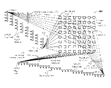
FIG. 1 illustrates a time-coherent network 100 comprising edge nodes,
collectively referenced as 120 and individually identified as 120(0),
120(1),..., 120(Q-1)
and switch units, collectively referenced as 160, logically arranged in a
matrix having v
rows and v columns. The rows of the matrix are indexed as row 0 to row (v-1),
where
row 0 is the bottom row and row (v-1) is the top row. The columns are indexed
as
column 0 to column (v-1), where column 0 is the leftmost column and column (v-
1) is
the rightmost column; v=8 in the exemplary network of FIG. 1.The switch units
160 are
individually identified as 160(j, k), j being a column identifier and k a row
identifier in the
matrix. An edge node 120 has a number of ingress channels 112 for receiving
data from
data sources, a number of egress channels 114 for transmitting data to data
sinks. An
edge node 120 has a number KV of upstream channels 122 connecting the edge
node
to v switch units 160, and a number K of downstream channels 124 connecting v
switch
units 160 to the edge node. The K upstream channels 122 connect the edge node
to a
switch unit 160 in each of the v columns. The downstream channels 124 connect
v
switch units, one from each of the v rows, to the edge node. Preferably x=v so
that an
edge node has one upstream channel 122 to each of v switch units 160 of
different
columns and one downstream channels from v switch units 160 of different rows.
To
simplify addressing and routing, the K downstream channels leading to the edge
node
originate from switch units belonging to one column.
An edge node 120 comprises a source node integrated with a sink node. For
clarity, each edge node 120 is indicated in FIG. 1 as a source-node side
having
upstream channels 122 and a sink-node side connecting to downstream channels
124.
It is understood, however, that a source-node side and a corresponding sink-
node side,
though illustrated as separate entities, together constitute one of the edge
nodes 120.
Each edge node 120 comprises an integrated switch fabric to switch data from
any
ingress channel 112 or any downstream channel 124 to any egress channel 114 or
any
18
CA 02916321 2015-12-29
upstream channel 122. An edge node 120 has ingress ports for receiving data
from
data sources, egress ports for transmitting data to data sinks, inbound ports
for
receiving signals from respective switch units 160 through downstream channels
124,
and outbound ports for transmitting signals to respective switch units 160
through
upstream channels 122.
In the network configuration of FIG. 1, edge node 120(0) has eight upstream
channels 122 to eight switch units 160(0,0) to 160(7,0) of row 0. Edge node
120(31) has
eight upstream channels 122 to eight switch units 160(0, 7) to 160(7,7) of row
7. Edge
node 120(0) has downstream channels 124 from eight switch units 160(0,0) to
160(0,7)
of column 0. Edge node 120(31) has downstream channels 124 from eight switch
units
160(7,0) to 160(7,7) of column 7.
FIG. 2 illustrates the connectivity of a set of edge nodes {120(20), ...,
120(23))
where each edge node in the set has eight upstream channels 122, one to each
of eight
switch units 160(0,5) to 160(7,5) and eight downstream channels 124, one from
each of
eight switch units 160(5,0) to 160(5,7).
FIG. 3 illustrates a time-coherent network 300 having a configuration similar
to
that of the time-coherent network 100 of FIG. 1 except that each of edge nodes
120 has
time-locked upstream channels 122 to switch units 160 of different rows and
different
columns of the matrix of switch units instead of time-locked upstream channels
122 to
switch units 160 of a single row. The downstream connectivity from switch
units 160 to
the edge nodes 120 is the same as that of network 100 of FIG. 1. In the
exemplary
configuration of FIG. 3, edge node 120(0) has eight upstream channels 122 to
eight
switch units 160(0,6), 160(1,0), 160(2, 1), 160(3,7), 160(4,2), 160(5,5),
160(6,3) and
160(7, 4). Edge node 120(31) has eight upstream channels 122 to eight switch
units
160(0, 0), 160(1,1), 160(2,4), 160(3,3), 160(4,6), 160(5,2), 160(6,5), and
160(7,7). The
downstream connectivity of edge nodes 120(0) and 120(31) is identical to that
of FIG. 1.
A major advantage of the network configuration of FIG. 1 or FIG. 3 is that
each
edge node 120 has a simple path to each other edge node 120 traversing a
single
19
CA 02916321 2015-12-29
switch unit 160. This greatly simplifies signaling, connection setup, and
connection
tracking. Several compound paths may be established between a source edge node
and a destination edge node. A compound path comprises two simple paths joined
at
an intermediate edge node 120. There are (2v-2) compound paths from any edge
node
120(j) to any other edge node 120(k), j#1. However, the (2v-2) compound paths
include partly overlapping paths. Each edge node has v upstream channels and v
downstream channels. Therefore, a maximum of (v-1) non-overlapping compound
paths may be established from any edge-node to any other edge node.
FIG. 4 illustrates a simple path 422 from an originating edge node 120(8) to a
destination edge node 120(31) traversing switch unit 160(7,1). An exemplary
compound
path 424 from originating edge node 120(8) to destination edge node 120(31) is
illustrated. Compound path 424 traverses switch unit 160(0,5), intermediate
edge node
120(0), and switch unit 160(7,4).
The network of FIG. 1 or FIG. 3 comprises a single matrix of switch units 160
forming a single core plane. Preferably, the switch units 160 are fast optical
switches. A
fast optical switch may be limited to medium dimensions, 64x64 for example. It
may be
desirable, however, to provide a parallel core plane using electronic switch
units. A
single-rotator latent space switch, to be described below with reference to
FIG. 48 to
FIG. 54, has a simple structure and scales to relatively large dimensions;
1024x1024 for
example.
FIG. 5 illustrates an edge node 120 having upstream channels 521 to switch
units 560 each of dimension mxm (m=12) arranged in a first matrix of columns
and
rows (for the case of 11=4). The edge node also has v upstream channels 522 to
v
switch units 160 each of dimension nxn (n=4) arranged in a second matrix of v
columns
and v rows (for the case of v=12). The edge node has downstream channels 523
from
switch units 560 and v downstream channels 424 from switch units 160. The edge
node
receives data from data sources through ingress channels 112 and transmits
data to
CA 02916321 2015-12-29
data sinks through egress channels 114. The total number of edge nodes is
vxn=pixm=48.
FIG. 6 illustrates downstream connectivity of the edge node 120 of FIG. 5
where
the edge node connects to pi. downstream channels 523 from switch units 560
of
column 3 of the first matrix and v downstream channels 524 to v switch units
160 in
column 0 of the second matrix.
FIG. 7 illustrates an alternative upstream connectivity of the edge node 120
of
FIG. 5 where the upstream channels 521 connect to switch units 560 in
different rows
and different columns in the first matrix and the upstream channels 522
connect to
switch units 160 in different rows and different columns in the second matrix.
FIG. 8 illustrates upstream connectivity of 12 edge nodes 120(0) to 120(11) to
the first matrix of FIG. 5. Each edge node has 4 upstream channels 521 to
switch units
560 in a row of the first matrix and 12 upstream channels 522 to switch units
160 in a
row of the second matrix. The total number of upstream channels from the 12
edge
nodes to the first matrix is 48 and the total number of upstream channels from
the 12
edge nodes to the second matrix is 192.
FIG. 9 illustrates upstream channels from the 12 edge nodes {120(0) to
120(11))
to the second matrix of FIG. 5. The upstream channels 522 connect to switch
units 160
of three rows The switch units 560 in a row of the first matrix collectively
connect to 48
upstream channels and, similarly, the switch units 160 in a row of the second
matrix
collectively connect to 48 upstream channels.
FIG. 10 illustrates downstream channels from the first matrix of switch units
of
the network of FIG. 5 to each of the 12 edge nodes 120(0) to 120(11). The 12
edge
nodes have downstream channels from switch units 560 of one column (column 0).
FIG. 11 illustrates downstream channels from the second matrix of switch units
of
the network of FIG. 5 to each of the 12 edge nodes 120(0) to 120(11). The 12
edge
21
CA 02916321 2015-12-29
nodes have downstream channels from switch units 160 of three columns (column
0,
column 1, and column 2).
GLOBAL COVERAGE
One may envisage a global network initially serving one billion users each
equipped to transmit and receive data at a rate of 100 megabits per second in
any
format; which is likely to be the network-user's expectation in the near
future. The
access capacity of such a network would be 100 petabits per second. With a
user
utilization factor of 0.1 for example, and with traffic efficiency of the
order of 0.8, the
network should have a core capacity (throughput) of at least 12.5 petabits per
second.
An edge node providing traffic-switching capacity of 10 terabits per second,
for
example, would support one million users, and only 1000 edge nodes of such
capacity
would be needed to serve a user population of one billion. However, with
Earth's land
area of 150 million km2, the use of only 1000 edge nodes may necessitate long
access
lines from the users' premises to the edge nodes, taking into account the
uneven
population distribution and the uninhabited areas. A more realistic number of
edge
nodes would be of the order of 50,000. Within the United States, 10000 edge
nodes
would be quite adequate to cover the land area of 9 million km2, and the
required
capacity of an edge node would vary from a hundred gigabits per second to tens
of
terabits per second.
Thus, in a network of global coverage, the number v of upstream channels 122
connecting an edge node 120 to v switch units 160 or downstream channels 124
connecting v switch units 160 to an edge node 120 may be significantly large;
1024 for
example. Each upstream channel 122 or downstream channel 124 is a wavelength
channel within a respective fiber-optic link. A group of upstream channels 122
occupying separate spectral bands may share a wavelength-division-multiplexed
(WDM) fiber link. Likewise, a group of downstream channels 124 occupying
separate
spectral bands may share a wavelength-division-multiplexed (WDM) fiber link.
Wavelength routers may be used to connect the edge nodes 120 to the switch
units 160
22
CA 02916321 2015-12-29
or 560 (FIG. 5) using a relatively small number of WDM links as will be
illustrated in FIG.
12 and FIG. 13.
FIG. 12 illustrates a network 1200 comprising edge nodes and switch units
arranged in one matrix, each edge node having upstream wavelength-division-
multiplexed (WDM) links to upstream wavelength routers and downstream WDM
links
from downstream routers, each upstream wavelength router having WDM links to
switch
units of one row and each downstream wavelength router having WDM links from
switch units of one column. The edge nodes 120 are individually identified as
120(0) to
120(Q-1), Q being the total number of edge nodes. The switch units 160 are
arranged
in a single matrix having v columns and v rows, each switch unit having n
input ports
and n output ports. Each edge node 120 comprises an edge controller as will be
described with reference to FIG. 20 and each switch unit 160 comprises a
switch-unit
controller as will be described with reference to FIG. 22. In the exemplary
network of
FIG. 12, v=8 and n=4, hence Q = vxn=32.
Upstream wavelength routers 1230 may be used to connect the edge nodes 120
to the switch units 160 and downstream wavelength routers 1250 may be used to
connect the switch units 160 to the edge nodes 120. For example, in a wide-
coverage
network, an upstream wavelength router 1230 may connect 32 upstream WDM links
1222 from a set of 32 edge nodes 120 to 32 WDM links 1224 leading to 32 switch
units
160. Each WDM link 1222 carries 32 wavelength channels from a single edge node
120 and each WDM link 1224 carries a wavelength channel from each edge node in
the
set of 32 edge nodes. Likewise, a downstream wavelength router 1250 may
connect 32
WDM links 1226 from 32 switch units 160 to 32 WDM links 1228 leading to 32
edge
nodes 120. Each WDM link 1228 carries channels directed to a single edge node
120.
Thus, with v=1024, an edge node 120 would have 32 upstream links 1222 leading
to 32
upstream wavelength routers 1230 and 32 downstream links 1228 from 32
downstream
wavelength routes 1250.
FIG. 13 illustrates a network similar to the network of FIG. 12 but with a
different
upstream connectivity. Each upstream wavelength router 1230 has WDM links to
switch
23
CA 02916321 2015-12-29
units in different rows and different columns. Each downstream wavelength
router 1250
has WDM links from switch units of one column as in the network of FIG. 12.
As will be described below, with reference to FIG. 20, an edge node 120 has
ingress ports, connecting to ingress channels 112, for receiving data from
data sources,
egress ports, connecting to egress channels 114, for transmitting data to data
sinks,
inbound ports, connecting to downstream channels 124, for receiving signals
from
respective switch units 160 through downstream wavelength routers 1250, and
outbound ports, connecting to upstream channels 122, for transmitting signals
to
respective switch units 160 though upstream wavelength routers 1230.
The connections of the upstream wavelength routers 1230 to the edge nodes
120 are configured so that each edge node 120 connects to a respective set of
v switch
units, one in each of the v columns. The connections of the downstream
wavelength
routers 1250 to the edge nodes 120 are configured so that each edge node 120
connects to a respective group of v switch units, one in each of the v rows.
Preferably,
each group of v switch units connecting to an edge node in the downstream
direction
belongs to a single column in the matrix of switch units.
With identical switch units 160, the number Q of edge nodes 120 is determined
by the dimension of a switch unit 160 and the number v of rows or columns in
the matrix
of switch units. With each switch unit having n inlet ports and n outlet
ports, the number
Q of edge nodes is determined as Q=vxn, and the number of switch units 160 is
v2.
A switch unit 160 may be: (1) a bufferless electronic space switch; (2) a
single-
rotator latent space switch (to be described below with reference to FIG. 48
to FIG. 54)
or (3) a fast switching optical space switch. Preferably, the switch units 160
of network
1200 are fast optical switches.
In the network of FIG. 12, an upstream wavelength router 1230 connects a
subset of edge nodes 120 to switch units 160 of one row. It may be desirable
to connect
the subset of edge nodes 120 to switch units in different rows and different
columns. In
24
CA 02916321 2015-12-29
the network of FIG. 13, upstream wavelength router 1230(0) connects the subset
of
edge nodes {120(0), 120(1), 120(2), 120(3)1 to eight switch units {160(0,1),
160(1,5),
160(2,7), 160(3,4), 160(4,6), 160(5,3), 160(6,0), 160(7,2)1 so that each edge
node in the
subset has one upstream channel to each of the eight switch units.
FIG. 14 illustrates exemplary connections of a group of 64 edge nodes 120
arbitrarily indexed as 120(0) to 120(63) each having 1024 upstream wavelength
channels to switch units 160 and 1024 downstream wavelength channels from
switch
units 160. The 1024 upstream wavelength channels emanating from an edge node
are
grouped into 16 upstream WDM links 1422 each WDM link multiplexing 64
wavelength
channels and terminating onto one switch unit 160. Likewise, the 1024
downstream
wavelength channels terminating on an edge node are grouped into 16 downstream
WDM links 1428 each WDM link 1428 multiplexing 64 wavelength channels, each
downstream WDM link emanating from one switch unit 160. Each switch unit 160
is of
dimension 64x64, having 64 input ports and 64 output ports, each input port
supporting
one upstream wavelength channel and each output port supporting one downstream
wavelength channel. Each switch unit 160 has a spectral demultiplexer at input
for
demultiplexing wavelength channels of an input WDM link and directing each
wavelength channel to a respective input port of the switch unit. Each switch
unit 160
has a spectral multiplexer at output for multiplexing output wavelength
channels onto an
output WDM link.
Sixteen upstream wavelength routers 1430, individually identified as 1430(0)
to
1430(15) are used to direct the 1024 upstream wavelength channels emanating
from
each of edge nodes 120(0) to 120(63) to 1024 different switch units 160,
subject to the
connectivity conditions described with reference to FIG. 1 and FIG. 3. A
wavelength
router 1430 connects to 64 upstream WDM links 1422 each carrying 64 wavelength
channels and 64 output WDM links 1424 each carrying one wavelength channel
from
each of the upstream WDM links.
CA 02916321 2015-12-29
Likewise, sixteen downstream wavelength routers 1450, individually identified
as
1450(0) to 1450(15) are used to direct downstream wavelength channels of 1024
WDM
links 1426 emanating from 1024 different switch units 160 to edge nodes 120(0)
to
120(63), so that each edge node 120 receives wavelength channels from switch
units
160 belonging to one column of the switch-unit matrix as described with
reference to
FIG. 1 and FIG. 3. A wavelength router 1450 connects to 64 WDM links 1426 each
carrying 64 wavelength channels and 64 downstream WDM links 1428 each carrying
one downstream wavelength channel from each of the 64 WDM links 1426.
FIG. 15 provides an overview of simple paths in the network of FIG. 12 or the
network of FIG. 13. Each simple path originates from a source edge node 120
and
terminates in a destination edge node 120. A simple path traverses an upstream
wavelength router 1230, a switch unit 160, and a downstream wavelength router
1250.
Time-Coordination
A switch unit 160 has a master time indicator which provides a time reference
to
be observed by each edge node 120 having an upstream channel to the switch
unit
160. The master time indicators of the v2 switch units are independent of each
other.
Each edge node 120 has v output ports connecting to v switch units in v
different
columns through upstream channels. An output port of an edge node 120 has a
slave
time indicator which time locks to a master time indicator of a switch unit
160 to which
the output port connects.
Data units arrive at the n inlet ports of a switch unit 160 at time instants
dictated
by a controller of the switch unit 160. The time instants are specified
according to a time
reference of the master time indicator of the switch unit (FIG. 22). Thus, no
signal
buffering is needed at the switch unit and the switching function at the
switch unit is time
coherent. A latent space switch has a constant transit delay specific to each
input-
output connection. However, an arriving data unit is not buffered at input and
the
switching function at the latent space switch is also time coherent.
26
CA 02916321 2015-12-29
Wavelength-routers configuration
FIG. 16 illustrates a configuration of upstream wavelength routers connecting
ten
edge nodes 120(0) to 120(9) to six switch units 160(0,2), 160(1, 0), 160(2,
1), 160(3, 5),
160(4, 3), and 160(5,4), belonging to different columns in a matrix of switch
units 160,
using wavelength routers 1625 each having at most four input WDM links 1622
and at
most four output WDM links 1624, where each output WDM link 1624 carries a
wavelength channel from each input WDM link 1622. Each switch unit 160 is of
dimension 10x10 (having 10 inlet ports and 10 outlet ports). The wavelength
routers
1625 are configured so that each edge node 120 has an upstream channel to each
of
the six switch units 160. As illustrated, six wavelength routers 1625(0) to
1625(5) of
dimensions (4x4), (4x2), (4x4), (4x2), (2x4), and (2x2) are used, where the
dimension
of a wavelength router is defined by the number of input WDM links and the
number of
output WDM links.
FIG. 17 illustrates a configuration of downstream wavelength routers 1725
connecting six switch units 160(2,0), 160(2,1), 160(2, 2), 160(2,3), 160(2,4),
and
160(2,5), all belonging to column 2, to the ten edge nodes 120(0) to 120(9)
using
wavelength routers 1725 each having at most four input WDM links 1724 and at
most
four output WDM links 1722, where each output WDM link 1722 carries a
wavelength
channel from each input WDM link 1724. Each switch unit 160 is of dimension
10x10
(n=10). The wavelength routers 1725 are configured so that each edge node 120
has a
downstream channel from each of the six switch units 160. As illustrated, six
wavelength routers 1725(0) to 1725(5) of dimensions (4x4), (4x2), (4x4),
(4x2), (2x4),
and (2x2) are used.
The maximum dimension of a wavelength router 1625 or 1725 in the exemplary
configurations of FIG. 16 and FIG. 17 is selected to be only 4x4 for clarity.
In a wide-
coverage network, wavelength routers each of a dimension of 32x32, for
example, may
be used.
27
CA 02916321 2015-12-29
FIG. 18 illustrates wavelength-channel assignments in a conventional
wavelength router. The figure illustrates an exemplary wavelength router 1800
of a
small dimension. Network 1200 (FIG. 12) would employ wavelength routers of
significantly larger dimensions. Exemplary wavelength router 1800 may be
employed as
an upstream wavelength router or a downstream wavelength router. Wavelength
router
1800 has eight input wavelength-division-multiplexed (WDM) links each carrying
a
multiplex of eight wavelength channels and eight output WDM links each
carrying a
wavelength channel from each input WDM link. The wavelength channels of a
first input
WDM links are denoted {Ao, A1, ..., A7}, the wavelength channels of a second
input
WDM link are denoted {Bo, B1, ..., 67}, and so on, where a character A, B,
..., identifies
an input WDM link and a subscript {0, 1, ..., 7} identifies a spectral band
allocated to a
respective wavelength channel. As illustrated, each output WDM link carries
channels
from different input WDM links and of different spectral bands.
FIG. 19 illustrates wavelength-channel assignments in a wavelength router
1900,
structurally identical to wavelength router 1800 except that only four output
WDM links
are used. Each input WDM channel carries four wavelength channels selected so
that
each of the four output WDM links carries eight wavelength channels of
different
spectral bands, one wavelength channel from each input WDM channel. As
illustrated
in FIG. 16 and FIG. 17, some wavelength routers may be partially provisioned
depending on the network configuration.
FIG. 20 illustrates an edge node 2000 for use in any of the networks of FIG.
1,
FIG. 3, FIG. 5, FIG. 7, FIG. 12, and FIG. 13. Edge node 2000 has a switch
fabric 2020,
an edge controller 2050, input ports, and output ports. The input ports
include ingress
ports 2026 for receiving data from data sources through ingress channels 112
and
inbound ports 2036 for receiving data from switch units through downstream
channels
124. The output ports include egress ports 2028 for transmitting data to data
sinks
through egress channels 114 and outbound ports 2038 for transmitting data to
switch
units through upstream channels 122.
28
CA 02916321 2015-12-29
Control signals from input ports 2026 and 2036 sent on control channels 2055
are time multiplexed in temporal multiplexer 2057 onto a channel 2062
connecting to
edge controller 2050. Control signals from edge controller 2050 to egress
ports 2028
and outbound ports 2038 are transferred through a channel 2082, a temporal
demultiplexer 2087 and channels 2085.
Each egress port 2028 is preferably paired with an ingress port 2026, and each
outbound port 2038 is preferably paired with an inbound port 2036. Control
signals from
the edge controller 2050 to the ingress ports 2026 and inbound ports 2036 may
be
transferred through corresponding paired output ports (egress ports and
outbound
ports).
Other arrangements for exchanging control signals between the edge controller
2050 and the input or output ports may be devised; for example the control
signals may
be transferred through the switch fabric instead of channels 2055 and 2085.
Edge controller 2050 schedules connections from input ports (ingress and
inbound ports) to output ports (egress and outbound ports) and instructs a
configuration
controller (slave controller) 2025 associated with the switch fabric 2020 to
establish
scheduled connections. Configuration controllers associated with switch
fabrics are well
known in the art. The edge controller 2050 is coupled to an edge time
indicator 2080
which distributes timing data to the outbound ports 2038. Each outbound port
adjusts
transmission time of data sent to a specific switch unit 160 according to the
time data
and time indications received from a master time indicator of the specific
switch unit.
The edge time indicator has the same periodicity and granularity of the master
time
indicator.
Control Time Slots
The time domain is organized into time frames each divided into a number T of
time slots of equal duration. Each connection (data stream) is allocated a
respective
number 6 of time slots per time frame, 0<a<T. A connection is preferably
confined to a
29
CA 02916321 2015-12-29
single upstream channel 122 from a source edge node 120 to a switch unit 160.
Control
time slots from edge controller 2050 to a switch-unit controller and vice
versa may be
transferred through dedicated control channels. A number A1 of upstream
control time
slots per time frame may be reserved in each upstream channel 122 from a
source
node 120 and a number A2 of downstream control time slots per time frame may
be
reserved in each downstream channel 124 from a switch unit 160. Although the
flow
rate of control signals generated by edge controller 2050 may differ from the
flow rate of
control signals generated by a switch-unit controller, it is preferable that
A1=A2.
As illustrated in FIG. 12, upstream channels 122 from an edge node 120 are
multiplexed onto an upstream WDM link 1222 connecting to a wavelength router
1230
and a downstream WDM link 1228 carries downstream channels 124 directed to an
edge node 120. Each inbound port 2036 of edge node 2000 has an optical-to-
electrical
converter and each outbound port 2038 has an electrical-to-optical converter
(not
illustrated). An edge node 120 may have a large number of upstream channels
122 and
downstream channels 124. Thus, upstream WDM link 1222 may actually comprise a
number of WDM links each carrying a smaller number of upstream channels 122.
For
example, with 1024 upstream channels 122 emanating from a single edge node 120
and 1024 downstream channels 124 terminating on the edge node, WDM link 1222
may
be implemented as 16 WDM links each multiplexing 64 upstream channels 122 and
WDM link 1228 may be implemented as 16 WDM links each multiplexing 64
downstream channels 124. Thus, an edge node 120 may have a number of spectral
multiplexers each for multiplexing outputs of a number of electrical-to-
optical convertors
onto an upstream WDM link and a number of spectral demultiplexers for
demultiplexing
optical signals received through a downstream WDM link. FIG. 21 illustrates an
edge
node 120 equipped with a number of spectral multiplexers 2123 and a number of
spectral demultiplexers 2125.
FIG. 22 illustrates a switch unit 160 for use in any of the networks of FIG.
1, FIG.
3, FIG. 5, FIG. 7, FIG. 12, and FIG. 13. The switch unit may have a photonic
or
electronic switching fabric 2262. Spectral demultiplexers 2225 (only one is
illustrated)
CA 02916321 2015-12-29
are employed at input and spectral multiplexers 2223 (only one is illustrated)
may be
employed at output. With an electronic fabric, optical-to-electrical
converters are
employed at input and electrical-to-optical converters are employed at output.
A fast-
switching optical switch fabric may be limited to a relatively small
dimension; 64x64, for
example.
A switch unit controller 2250 may be accessed through the switch fabric 2262
or
through other arrangements known in the art. The switch controller 2250
receives
connection requests from edge nodes 120, allocates time slots for each
connection, and
communicates relevant information to the edge nodes 120. A switch unit 160
does not
buffer payload signals received from the edge nodes 120. Thus, to enable time-
coherent switching, at a switch unit 160, of signals received from multiple
edge nodes
120, outbound ports 2038 of the edge nodes are time-locked to the switch unit
160. The
switch unit controller 2250 is coupled to a master time indicator 2280 and
exchanges
time indications with edge time indicator 2080 to time-lock outbound ports
2038 of each
subtending edge node to the switch unit 160. FIG. 23 illustrates exchange of
time
indications between a master time indicator 2280 of a switch unit 160 and edge
time
indicators (2080(0), 2080(1)....., 2080(63)) to enable coherent switching at a
switch unit
in any of the networks of FIG. 1, FIG. 3, FIG. 5, FIG. 7, FIG. 12, and FIG.
13.
The edge controller 2050 has an edge processor and an edge scheduling
module which includes a memory device storing processor executable
instructions
which cause the edge processor to implement time-locking and scheduling
functions of
an edge node. The switch unit controller 2250 has a switch-unit processor and
a switch-
unit scheduling module which includes a memory device storing processor
executable
instructions which cause the processor to implement time-locking and
scheduling
functions of a switch unit.
Exemplary edge-node structure
FIG. 24 illustrates ordinary and transposed connections of a first set of
ports
2410 having a number N>2 of ports and a second set of ports 2420 having N
ports; N
31
CA 02916321 2015-12-29
=
equals12 in the exemplary case of FIG. 24. The N ports of the first set are
indexed as 0,
1, ..., (N-1), and the N ports of the second set are likewise indexed as 0, 1,
..., (N-1).
Thus, the ports of the first set are individually identified as {2410(0),
2410(1).....
(2410(N-1)) and the ports of the second set are individually identified as
{2410(0),
2410(1)....., (2410(N-1)1. The ports of the first set have one-to-one static
connections
to the ports of the second set. The first set of ports is said to have
ordinary connections
to the second set of ports if each port 2410(j) is connected to a likewise
indexed port
2420(j), Ol<N. The first set of ports is said to have transposed connections
of order L to
the second set of ports if each port 2410(j) is connected to a port 2420ILHI,
OA<N,
01._<N, where IXI denotes Xmodulo N, i.e., VI = X, if XA, and X=(N¨X), if X<0.
Thus,
IL¨jI=L¨j, if and IL¨ji= (N¨L+j), if L<j.
Four connection patterns are illustrated in FIG. 24. In a first pattern, the
first set
of ports 2410 has ordinary connections 2480 to the second set of ports 2420.
In a
second pattern, the first set of ports 2410 has transposed connections of
order 0 to the
second set of ports 2420. In a third pattern, the first set of ports 2410 has
transposed
connections of order 4 to the second set of ports 2420. In a fourth pattern,
the first set of
ports 2410 has transposed connections of order (N-1) to the second set of
ports 2420.
Single-Rotator Circulating Switch
FIG. 25 illustrates an exemplary single-rotator circulating switch 2500
disclosed
in United States Patent 7,567,556. Circulating switch 2500 comprises eight
switch
elements 2530 and a single rotator 2550 having eight inlets 2524 and eight
outlets
2526. Each switch element 2530 receives data from data sources (not
illustrated)
through an ingress channel 2502 and transmits data to data sinks (not
illustrated)
through an egress channel 2504. Each switch element connects to a respective
inlet
2524 of rotator 2550 through an output channel 2506 and connects to a
respective
outlet 2526 of rotator 2550 through an input channel 2508. Each ingress
channel 2502
has a capacity R bits per second, each egress channel 2504 has a capacity R,
each
32
CA 02916321 2015-12-29
output channel 2506 has a capacity of 2R and each input channel 2508 has a
capacity
of 2R. A typical value of R is 10 gigabits per second (Gb/s).
Switch elements 2530 are individually identified by indices 0, 1, ..., (N-1),
where
N=8 in the exemplary circulating switch 2500. An inlet 2524 connecting to a
switch
element of index j, 0A<N is further identified by the index j as 2524(j) and
an outlet 2526
connecting to a switch element of index j is further identified by the index j
as 2526(j).
Thus the inlets 2524 are referenced as 2524(0) to 2524(N-1) and the outlets
2526 are
referenced as 2526(0) to 2526(N-1). For brevity, a switch element 2530 of
index j may
be referenced as switch element j, an inlet 2524 of index j may be referenced
as inlet j,
and an outlet 2526 of index j may be referenced as outlet j.
Rotator 2550 may be an ascending rotator or a descending rotator. An ascending
rotator 2550 connects an inlet j to an outlet {j-Ft}moduio N during time slot
t of a repetitive
time frame organized into N time slots. A descending rotator 2550 connects an
inlet j to
an outlet {j¨t}modulo N during time slot t.
During time slot t, a switch element of index j may transfer data to a switch
element x={.1 t}moduk, N through an ascending rotator 2550. Thus, t={¨j}
modulo N. If the
transferred data is destined to a switch element k, k#x, the data is held in
switch
element x until inlet x connects to outlet k. Thus, a data unit written in
switch element x
during time slot t is transferred to switch element k during a time slot t
where
T={k¨x}modwo N, and the delay D in transit switch element x is determined as
D=1¨t=(k+j-2x}moduio N. Thus, data transferred from switch element j to switch
element k
may be held in a transit switch element x for a period of time determined by
j, k, and x.
A transit switch element 2530(x) may be any switch element 2530 other than the
originating switch element 2530(j) and the destination switch element 2530(k).
Data
units of a data stream from switch element j to switch element k may use more
than one
transit switch element x and because of the dependency of the delay D on the
transit
switch elements, the data units may not be received at switch element k in the
order in
which the data units were sent from switch element j. Thus, data reordering at
a
33
CA 02916321 2015-12-29
receiving switch element 2530 is needed as described in the aforementioned
United
States Patent 7,567,556.
FIG. 26 illustrates a first configuration of a single-rotator circulating
switch 2600
employing transposed connections in order to preserve sequential order of data
segments of each data stream. Circulating switch 2600 comprises eight switch
elements 2630 and a single rotator 2650 having eight inlets 2624 and eight
outlets
2626. Each switch element 2630 receives data from data sources (not
illustrated)
through an ingress channel 2602 and transmits data to data sinks (not
illustrated)
through an egress channel 2604. Each switch element 2630 connects to a
respective
inlet 2624 of rotator 2550 through an output channel 2606 and connects to a
respective
outlet 2626 of rotator 2650 through an input channel 2608. Each ingress
channel 2602
has a capacity R, each egress channel 2604 has a capacity R, each output
channel
2606 has a capacity of 2R and each input channel 2608 has a capacity of 2R.
Switch elements 2630 are individually identified by indices 0, 1, ..., (N-1),
where
N=8 in the exemplary circulating switch 2600. An inlet 2624 connecting to a
switch
element of index j, Ol<N is further identified by the index j as 2624(j) and
an outlet 2626
connecting to a switch element of index j is further identified by the index j
as 2626(j).
Thus the inlets 2624 are referenced as 2624(0) to 2624(N-1) and the outlets
2626 are
referenced as 2626(0) to 2626(N-1).
Switch elements 2630 have ordinary connections to inlets 2624 where a switch
element 2630(j) connects to inlet 2624(j), 0A<N. However, outlets 2626 have
transposed connections to switch elements 2630 where an outlet 2626(j)
connects to
switch element 2630 of index (L¨Dmodulo N, OA<N, where L=7 in the exemplary
network
2600. The use of the transposed connections ensures proper sequential order of
data
segments of each data stream, where a data stream is defined according to an
originating switch element 2630 and a terminating switch element 2630.
FIG. 27 illustrates a configuration of a single-rotator circulating switch
2700 in
which switch elements 2630 have transposed connections to inlets 2624 where a
switch
34
CA 02916321 2015-12-29
element 2630(j) connects to inlet 2624 of index (L¨)modulo N, Ol<N, L=7.
However,
outlets 2626 have ordinary connections to switch elements 2630 where an outlet
2626(j)
connects to switch element 2630(j), 0<j<N. The use of the transposed
connections
ensures proper sequential order of data segments of each data stream.
FIG. 28 illustrates an exemplary single-rotator circulating switch 2800 which
comprises five switch elements 2830 and a single rotator 2845 having five
inlets 2844
and five outlets 2846. Each switch element 2830 receives data from data
sources (not
illustrated) through an external input channel 2802 and transmits data to data
sinks (not
illustrated) through an external output channel 2804. Each switch element
connects to a
respective inlet 2844 of rotator 2845 through two internal output channels
2816 and
2818, and connects to a respective outlet 2846 through two internal input
channels
2826 and 2828. Each of external input channels 2802, external output channels
2804,
internal output channels 2816, 2818, and internal input channels 2826, 2828
has the
same capacity of R bits/second (for example R=10 Gb/s). Each switch unit 2830
has an
external input port for receiving data through external channel 2802, an
external output
port for transmitting data through external channel 2804, two internal output
ports for
transmitting data through internal output channels 2816 and 2818, and two
internal input
ports for receiving data through internal input channels 2826 and 2828. Each
port of a
switch unit may include a short buffer sufficient to hold one data unit (data
segment).
An inlet selector 2835 is provided at each inlet 2844 and an output selector
2855
is provided at each outlet 2846. An inlet selector 2835 has two inlet ports
2842 and
2843 alternately connecting one of two channels 2816 and 2818 originating from
a
respective switch element 2830 to an inlet 2844. An outlet selector 2855 has
two outlet
ports 2848 and 2849 alternately connecting an outlet 2846 to one of two
channels 2826
and 2828 terminating on a respective switch element 2830.
Switch elements 2830 are individually identified by indices 0, 1, ..., (N-1),
where
N=8 in the exemplary circulating switch 2800. In general, the number N of
switch
elements exceeds 2 and may have an upper bound dictated by transit delay. A
practical
CA 02916321 2015-12-29
upper bound of N would be of the order of 2000. An inlet 2844 connecting to a
switch
element of index j, 0.1<N is identified by the index j as 28440) and an outlet
2846
connecting to a switch element of index j is identified by the index j as
2846(j).
The switch elements 2830 have ordinary connections to the inlets 2844 so that
a
switch element 28300) connects to a selector 2835 of inlet 2844(j). The
outlets 2846
have transposed connections to the switch elements 2830 so that a selector
2855 of
outlet (1----Dmodulo N connects to switch element 2830(j). In the exemplary
configuration of
FIG. 28, 0A<N, O_L<N, and L=7. For brevity, hereinafter, a switch element 2830
of
index j may be referenced as switch element j, an inlet 2844 of index j may be
referenced as inlet j, and an outlet 2846 of index j may be referenced as
outlet j.
Using an ascending rotator 2845, inlet j connects to outlet x, where
x={j+t}moduio N
during time slot t. Thus, t={x¨}moduio N. Outlet x connects to switch element
(L¨x).
During time slot t, switch element j may transfer data to a switch element
(L¨x). If the
transferred data is destined to a switch element k, k#x, the data is held in
switch
element (L¨x) until inlet (L¨x) connects to outlet (L¨k), noting that outlet
(L¨k) connects
to switch element k. Thus, a data unit written in switch element (L¨x) during
time slot t is
transferred to outlet (L¨k) during a time slot I where t={ )(,--k} modulo N.
The delay D in
transit switch element x is determined as D=T¨t=(j¨k}modub N. Thus, data
transferred from
switch element j to outlet k may be held in a transit switch element (N¨x) for
a period of
time D which is independent of x and determined only by j and k.
Data units of a data stream from switch element j to switch element k may use
more than one transit switch element x and because of the independence of the
transit
delay D of the transit switch element x used, data units from switch element j
are
received at switch element k in the order in which the data units were sent
from switch
element j.
Notably, in the configuration of FIG. 28, switch element j connects to both
inlet
ports 2842 and 2843 of an inlet selector 2835 of inlet j and switch element j
connects to
36
CA 02916321 2015-12-29
both outlet ports 2848 and 2849 of an outlet selector 2855 of outlet (N¨j). A
data stream
from switch element j to switch element k, 0A<N, Ok<N, k#j, may be routed
through
either of two simple paths. A first simple path traverses a channel 2816 to
inlet j and a
channel 2826 from outlet (L¨k) to switch element k. A second simple path
traverses a
channel 2818 to inlet j and a channel 2828 from outlet (L¨k) to switch element
k. The
two simple connections take place during time slot t={L¨j¨k}modwo N. The data
stream
from switch element j to a switch element k may also be routed through either
of two
sets of compound paths. A path in the first set traverses a channel 2816 from
switch
element j to inlet j, a channel 2826 from an outlet x, (Xx<N, x#j, to switch
element (L¨x),
a channel 2816 from switch element (L¨x) to inlet (L¨x), and a channel 2826
from outlet
(L¨k) to switch element k. A path in the second set traverses a channel 2818
from
switch element j to inlet j, a channel 2828 from outlet x to switch element
(L¨x), a
channel 2818 from switch element (L¨x) to inlet (L¨x), and a channel 2828 from
outlet
(L¨k) to switch element k. The transit delay D is determined as D={j¨k}moduio
N for either
of the two paths and the configuration 2800 provides uniphase paths for a pair
of
originating and destination switch units 2830.
FIG. 29 illustrates an alternate configuration of the uniphase single-rotator
circulating switch of FIG. 28 where the switch elements 2830 have transposed
connections to the inlets 2844 so that a switch element 2830(j) connects to a
selector
2835 of inlet 2844 of index (L¨)modulo N. In the exemplary configuration of
FIG. 29, Ol<N,
0__L<N, and L=7. The outlets 2846 have ordinary connections to the switch
elements
2830 so that a selector 2855 of outlet (j) connects to switch element 2830(j).
FIG. 30 illustrates a configuration 3000 in which the switch elements 2830
have
ordinary connections to inlet ports 2842 of inlet selectors 2835 and
transposed
connections to inlet ports 2843 of inlet selectors 2835. Outlet ports 2848 of
outlet
selectors 2855 have transposed connections to the switch units 2830 and outlet
ports
2849 of outlet selectors 2855 have ordinary connections to the switch units
2830.
Thus, a switch element 2830(j) connects to inlet port 2842 of an inlet
selector 2835 of
37
CA 02916321 2015-12-29
inlet 2844(j) through a channel 2816 and inlet port 2823 of inlet selector
2835 of inlet
28441L¨j1, where IL¨jidenotes (LH) modulo N, through a channel 2818, 0A<N,
L=7. Outlet
port 2848 of an outlet selector 2855 of outlet 2846(j) connects to switch
element
28301L¨ji through a channel 2826 and outlet port 2849 of an outlet selector of
outlet
2846(j) connects to switch element 1830(j) through a channel 2828.
A data stream from switch element j to switch element k, Ol<N,
k#j, may
be routed through either of two simple paths. A first simple path traverses a
channel
2816 to inlet j and a channel 2826 from outlet (L¨k) to switch element k. A
second
simple path traverses a channel 2818 to inlet (L¨j) and a channel 2828 from
outlet k to
switch element k. The first simple connection takes place during time slot
t={L¨j¨k}moduio
N and the second simple connections takes place during time slot
t={j+k¨L}moduio N. The
data stream from switch element j to a switch element k may also be routed
through
either of two sets of compound paths. A path in the first set traverses a
channel 2816
from switch element j to inlet j, a channel 2826 from an outlet x, CXx<N, x#j,
to switch
element (L¨x), a channel 2816 from switch element (L¨x) to inlet (L¨x), and a
channel
2826 from outlet (L¨k) to switch element k. A path in the second set traverses
a channel
2818 from switch element j to inlet (L¨j), a channel from an outlet x to
switch element
(L¨x), a channel 2818 from switch element (L¨x) to inlet x, and a channel 2828
from
outlet (L¨k) to switch element k. The transit delay is D={j¨k}moduio N for the
first path and
D={k¨}moduto N for the second phase. Thus configuration 3000 provides two-
phase paths
for each pair of originating and destination switch units 2830 and a
controller of the
originating switch element 2830 may select a path of lower transit delay. The
first set of
path is preferred if {j¨k}modulo N is less than L(N+1)/2 J, where Lyi denotes
the integer part
of any real number y; otherwise the second set of paths is preferred. For
example, with
j=6 and k=0, any compound path in the first set of paths has a transit delay
D1={6-0}moduio 8= 6 time slots and any compound path in the second set of
paths has a
transit delay Di ={0-6}modulo 8= 2 time slots; the second path may be
selected.
38
CA 02916321 2015-12-29
FIG. 31 illustrates a first connectivity of the two-phase single-rotator
circulating
switch of FIG. 30 sustaining the first set of compound paths described above.
The first
connectivity is effective during a first part of a time slot.
FIG. 32 illustrates a second connectivity of the two-phase single-rotator
circulating switch of FIG. 30 sustaining the second set of compound paths
described
above. The second connectivity is effective during a second part of a time
slot.
FIG. 33 illustrates a two-phase single-rotator circulating switch 3300 having
an
arbitrary number N>2 of switch elements and preserving sequential order of
data
segments of each data stream. The N switch elements have ordinary connections
to N
inlet ports 2842, transposed connections to N inlet ports 2843, transposed
connections
from N outlet ports 2848, and ordinary connections from outlet ports 2849.
FIG. 34 illustrates a control system of the single-rotator circulating switch
of FIG.
33. Each switch element 2830 has an element controller 3470 which communicates
with
an edge controller 3450. A control time frame is organized into N equal
control time
slots with each control time slot allocated to a respective switch-element
controller 3470
for two-way communications with the edge controller 3450. A switch element
controller
3470 may be allocated a specific control time slot for transmitting control
signals to the
edge controller 3450 and a different control time slot for receiving control
signals from
the edge controller.
FIG. 35 illustrates a two-phase single-rotator circulating switch having five
switch
elements 2830 with transposed connections of order 4, and employing a
controller 3580
accessible through the single rotator. Each switch element is allocated a time
slot for
communicating with the controller 3580.
FIG. 36 illustrates a two-phase single-rotator circulating switch with an
arbitrary
number N>2 of switch elements having transposed connections of order L=(N-1)
and
employing a controller accessible through the single rotator. Each switch
element is
allocated a time slot for communicating with the controller 3680.
39
CA 02916321 2015-12-29
FIG. 37 tabulates data-transfer timing of the two-phase single-rotator
circulating
switch of FIG. 33. With static ordinary connections from the switch elements
to single
rotator and static transposed connections from the single rotator to the
switch elements,
a switch element j connects to inlet j (inlet port 2842(j)) and with an
ascending rotator
2845, inlet j connects to outlet (j-'-t1) during a first part of a time slot
t1, (=l_t-I<N. Outlet
(j+ti) connects to a transit (intermediate) switch element 2830 of index (L¨(j-
Ft1)). Switch
element (L¨(j-Ft1)) has a channel to inlet port 2842 of inlet (L¨(j-Fti)). In
order to reach
destination switch element 2830(k), transit data in switch element (L¨(j1-ti))
is
transferred from inlet (L¨(j-Fti)) to outlet (L¨k) during a time slot t2=
(L¨k)-
(L¨(j+t1))=(j-10-t1). Thus, the transit delay is t2¨t1=j¨k.
Likewise, with static transposed connections from the switch elements to
single
rotator and static ordinary connections from the single rotator to the switch
elements, a
switch element j connects to inlet (L¨j) and with an ascending rotator 2845,
inlet (L¨j)
connects to outlet (L¨j -Ft1) during a first part of a time slot t1, Citi<N.
Outlet (LH +ti)
connects to a transit (intermediate) switch element 2830 of index (L¨j+ti).
Switch
element (L¨j-Fti) has a channel to inlet port 2842 of inlet 04). In order to
reach
destination switch element 2830(k), transit data in switch element (L¨j+ti) is
transferred
from inlet a-ti) to outlet k during a time slot t2= k¨ Hi. Thus, the transit
delay is
t2¨t1=k¨j.
During a rotation cycle, each inlet of rotator 2845 connects to each outlet
during
a time slot of predefined duration. Thus, rotator 2845 completes a rotation
cycle of N
time slots. Controller 3680 receives control signals from the switch elements
2830,
schedules exchange of data among the switch elements, and communicates data-
transfer schedules to the switch elements 2830. A scheduling time frame having
a
number F of time slots may be used to facilitate data-transfer scheduling. The
number F
is at least equal to the number N of rotator inlets which is also the number
of time slots
in a rotation cycle. To simplify communications between controller 3680 and
individual
controllers (not illustrated) of the switch elements 2830, the switch elements
may be
allocated non-overlapping control time slots within the scheduling time frame.
With a
CA 02916321 2015-12-29
large value of N, 1024 for example, the number F of time slots in a scheduling
time
frame may be selected to equal the number N of time slots of the rotation
cycle.
However, the number F may be any arbitrary integer exceeding N, and may
substantially exceed N.
FIG. 38 illustrates an exemplary allocation of control time slots for the two-
phase
single-rotator circulating switch of FIG. 36 for a case where F=N=12. The
controller
3680 has a channel 2816 to inlet 2844(N-1), a channel 2818 to inlet 2844(0), a
channel
2826 from outlet 2846(0), and a channel 2828 from outlet 2846(N-1). Controller
3660
replaces switch element 2830(N-1). Each switch element 2830(j), 01<(N-2), has
a first
path to controller 3680 traversing channels 2816 and 2826, and a second path
traversing channels 2818 and 2828. As illustrated in FIG. 37, a switch element
2830(j)
has a first path to a switch element 2830 of index {L¨j¨tl}modulo N, and a
second path to a
switch element 2830 of index 11--j+t1lmodulo N, during a time slot t1,
The time slot t during which the first path from switch element 2830(j) to the
controller 3680 is established is determined from {L¨j---r}modulo N= (N-1).
The
configuration of FIG. 36 uses transposed connections of order L=(N-1). Thus,
t={-j}
modulo N=(N¨D. The time slot during which the second path from switch element
2830(j)
to the controller 3680 is established is determined from {L 4}rnodulo N= (N-
1). Thus,
Time slot is allocated as a control time slot 3882 and time slot 4 is
allocated as a
control time slot for switch element 2830(j). Thus, switch elements 2830(0),
2830(1),
2830(2)...., 3830(N-3), and 2830(N-2), have paths through channels 2816 and
2826 to
the controller 3680, during control time slots 3882 of indices 0, (N-1), (N-
2), , 3, and
2, respectively, and paths through channels 2818 and 2828 to the controller
3680 during
control time slots 3884 of indices 0, 1, 2 , , (N-2), and (N-1),
respectively.
Single-Rotator Latent-Space Switch
FIG. 39 illustrates a known rotating access packet switch (United States
Patents
5,168,492, 5,745,486, and Publication 2006/0123162) comprising a latent space
switch
41
CA 02916321 2015-12-29
3920, input buffers 3912 and output buffers 3914. The latent space switch 3920
comprises an input rotator 3925 having N inlets 3924 and N outlets 3926 and an
output
rotator 3945 having N inlets 3944 and N outlets 3946; N=8 in the illustrated
exemplary
rotating-access switch. A bank of N transit memory devices 3950 connects to
the N
outlets 3926 of input rotators 3925 and N inlets 3944 of output rotator 3945.
A controller
3980 is connected to an outlet 3946 of output rotator 3945 and an inlet 3924
of input
rotator 3925 leaving (N-1) inlets 3924 of input rotator 3925 to connect to (N-
1) input
buffers 3912 and (N-1) outlets 3946 of output rotator 3945 to connect to (N-1)
output
buffers 3914. One of the two rotators 3925 and 3945 is an ascending rotator
and the
other is a descending rotator. The input buffers are individually identified
as 3912(j),
0A<N. Likewise output buffers 3914 are individually identified as 3914(j) and
transit
memory devices 3950 are individually identified as 3950(j), 0A<N. During a
time slot t
in a repetitive time frame having N time slots, input rotator 3925 connects
input buffer j
to transit memory device {j+13xt}modub N, and output rotator 3945 connects
transit memory
device j to output buffer (j-13xt) modulo N where pi if rotator 3925 is an
ascending rotator
and rotator 3945 is a descending rotator and p¨i if rotator 3925 is a
descending
rotator and rotator 3945 is an ascending rotator. A data unit transferred from
an input
buffer 3912(j) to an output buffer 3914(k) through any transit memory device
3950 is
delayed in the transit memory device 3950 for a period of {j¨k}moduio N, if
rotator 3925 is
an ascending rotator and rotator 3945 is a descending rotator, or delayed for
a period of
{k¨Dmodulo N, if rotator 3925 is a descending rotator and rotator 3945 is an
ascending
rotator.
FIG. 40 illustrates a latent space switch 4020 comprising an input rotator
4045
having N inlets 4044 and N outlets 4046 and an output rotator 4055 having N
inlets
4054 and N outlets 4056; N=8 in the illustrated latent space switch. A bank of
(N-1)
transit memory devices 4050 connects to (N-1) outlets 4046 of input rotator
4045 and
(N-1) inlets 4054 of output rotator 4055. A controller 4080 is connected to an
outlet
4046 of input rotator 4045 and an inlet 4054 of output rotator 4055. As in
latent-space
switch 3920, one of the two rotators 4045 and 4055 is an ascending rotator and
the
42
CA 02916321 2015-12-29
other is a descending rotator. The inlets 4044 are individually identified as
4044(j),
0A<N. Likewise outlets 4056 are individually identified as 4056(j) and transit
memory
devices 4050 are individually identified as 4050(j), Ol<N. During a time slot
tin a
repetitive time frame having N time slots, input rotator 4045 connects inlet
4044(j) to
transit memory device {j-F13xt}moduz N, and output rotator 4055 connects
transit memory
device j to outlet 4056(k), k={j¨f3xt}moduioN, where 3=1 if rotator 4045 is an
ascending
rotator and rotator 4055 is a descending rotator and 3=-1 if rotator 4045 is a
descending rotator and rotator 4055 is an ascending rotator. A data unit
transferred
from an inlet 4044(j) to an outlet 4056(k) through any transit memory device
4050 is
delayed in the transit memory device 4050 for a period of {j¨k}modulo N, if
rotator 4045 is
an ascending rotator and rotator 4055 is a descending rotator, or delayed for
a period of
{k¨j}moduk, N, if rotator 4045 is a descending rotator and rotator 4045 is an
ascending
rotator.
An ingress port 4040 connecting to inlet 4044 dedicates a time slot within the
time frame for receiving control signals from respective external sources and
transferring the control signals to controller 4080. An egress port 4060
connecting to an
outlet 4056 dedicates a time slot within the time frame for transmitting
control signals
from controller 4080 to respective external sinks.
Latent space switch 3920 uses N transit memory devices 3950 and supports
(N-1) ingress ports and (N-1) egress ports. A control data unit transferred
from an
ingress port to controller 3980 is first written in a transit memory device
3950 then
transferred to controller 3980. A control data unit transferred from
controller 3980 to an
egress port is first written in a transit memory device 3950 then transferred
to the egress
port. Latent space switch 4020 uses (N-1) transit memory devices 4050,
supports N
ingress ports and N egress ports, and simplifies access to the controller
4080.
During a first part of a time slot, data is transferred from inlets 4044 to
controller
4080 and to transit memory devices 4050 through input rotator 4045. During a
second
part of the time slot, data is transferred from controller 4080 and transit
memory devices
43
CA 02916321 2015-12-29
4050 to outlets 4056 through output rotator 4055. The two rotators 4045 and
4055 may,
therefore, be replaced by a single rotator. However, rotators 4045 and 4055
should
rotate in opposite directions, one being an ascending rotator and the other a
descending
rotator, in order to guarantee a transit delay for a path from an inlet
4044(j) to an outlet
4056(k) which is independent of the transit memory device 4050 used and
depends only
on the indices j and k.
A single rotator may be devised to be an ascending rotator during a first part
of
each time slot and a descending rotator during a second part of each time
slot.
Preferably, in accordance with an embodiment of the present invention, the
connectivity
of the transit memory devices to the input side and output side of a single
rotator
rotating in one direction, either ascending or descending, may be configured
to realize
delay independence of the transit memory devices traversed by a data stream.
FIG. 41 illustrates a latent space switch 4120 comprising a first ascending
rotator
4125 having eight inlets 4124 and eight outlets 4126, a bank of eight transit
memory
devices 4150, and a second ascending rotator 4145 having eight inlets 4144 and
eight
outlets 4146. The eight outlets 4126 of the first ascending rotator have
static
transposed connections of order 0 to the bank of transit memory devices 4150,
and the
bank of transit memory devices 4150 has ordinary connection to the inlets 4144
of the
second ascending rotator. The inlets 4124 of the first ascending rotator may
have
ordinary connections to ingress ports 4140 and the outlets 4146 of the second
ascending rotator may have ordinary connections to egress ports 4160.
An inlet 4124(j) of the first ascending rotator connects to outlet 41261j+til,
where
Ii-Ftil denotes (+ti)modulo N, during a time slot t1, C)ti<N. Outlet 4126Ij+ti
I connects to a
transit memory device 4150IL¨(j+t1)j. Transit memory device IL¨(j+ti)I
connects to inlet
41441L¨(j-Fti)1 of the second ascending rotator. In order to reach outlet
4146(k) of the
second ascending rotator, transit data in transit memory device 41501L¨(j+WI
is
transferred from inlet 41441L¨(j+ti)I to outlet 4146(k) during a time slot
t2=1k¨
(L¨(j+ti))1=1j+k¨L+t1l. Thus, the transit delay is t2¨ti=lj+k¨LI, which is
independent of the
transit memory device used. The transit delay depends on the indices j and k
of the
44
CA 02916321 2015-12-29
ingress and egress ports and the order L, 0.1_<N, of the transposed
connection, which
is a fixed parameter for a specific configuration of a latent space switch
4120. The value
of L is 0 in the configuration of FIG. 41.
To render the delay from an ingress port 4112(j) to an egress port 4146(k),
Ol<N,Ok<N, independent of the transposition order L, the outlets 4146 of the
second
ascending rotator may have transposed connections of the same order L to the
egress
ports. Thus, in order to reach egress port 4114(k), transit data in transit
memory device
41501L¨(j+ti)I is transferred from inlet 4144IL¨(j+t1)I to outlet 41461L¨kl
during a time
slot t2= I(L¨k)¨ (L¨(j+t1))1=Ij¨k -Ft1I, and the transit delay is t2--
t1=1j¨kl, which is
independent of the transposition order L.
FIG. 42 illustrates a latent space switch 4220 comprising a first ascending
rotator
4125 having eight inlets 4124 and eight outlets 4126, a bank of eight transit
memory
devices 4150, and a second ascending rotator 4145 having eight inlets 4144 and
eight
outlets 4146. The eight outlets 4126 of the first ascending rotator have
static ordinary
connections to the bank of transit memory devices 4150, and the bank of
transit
memory devices 4150 has transposed connections to the inlets 4144 of the
second
ascending rotator. The inlets 4124 of the first ascending rotator may have
ordinary
connections to ingress ports 4140 and the outlets 4146 of the second ascending
rotator
may have ordinary connections to egress ports 4160.
An inlet 4124(j) of the first ascending rotator connects to outlet 41261j+t11
during a
time slot t1, Outlet 41261j-Ftll connects to a transit memory device
4150Ij+t1
Transit memory device 4150Ij+ti I connects to inlet 41441L¨(j+t1)1 of the
second
ascending rotator. In order to reach outlet 4146(k), transit data in transit
memory
device 41501j+til is transferred from inlet 41441L¨(j+t1)1 to outlet 4146(k)
during a time
slot t2=Ik¨ (L¨(j-Fti))1=1j+k¨L-Ft1l. Thus, the transit delay is t2¨ti=lii-
k¨LI. The value of L is
0 in the configuration of FIG. 42.
To render the delay from an ingress port 4140(j) to an egress port 4160(k),
Ol<N, 0.1<<N, independent of the transposition order L, the outlets 4146 of
the second
CA 02916321 2015-12-29
ascending rotator may have transposed connections of the same order L to the
egress
ports 4160, resulting in a transit delay of lj¨kl.
FIG. 43 illustrates a latent space switch similar to the latent space switch
of FIG.
41 but with the first ascending rotator having transposed connections of order
7 to a
bank of transit memory devices. The transit delay for a connection from an
ingress port
4112(j) to an egress port 4114(k) is then lj+k-71 if the outlets 4146 of the
second
ascending rotator have ordinary connections to the egress ports 4160. With
transposed
connections of order 7 from the outlets 4146 of the second ascending rotator
to the
egress ports 4160, the transition delay from an ingress port 4140(j) to an
egress port
4160(k) is lj¨k!.
FIG. 44 illustrates a latent space switch similar to the latent space switch
of FIG.
42 but with the bank of transit memory devices having transposed connections
of order
7 to the inlets 4144 of the second ascending rotator. The transit delay for a
connection
from an ingress port 4112(j) to an egress port 4114(k) is then lj+k-71 if the
outlet 4146 of
the second ascending rotator have ordinary connections to the egress ports
4160. With
transposed connections of order L from the outlets 4146 of the second
ascending
rotator to the egress ports 4160, the transition delay from an ingress port
4112(j) to an
egress port 4114(k) is lj¨k!.
FIG. 45 illustrates a latent space switch similar to the latent space switch
of FIG.
41 but with the first ascending rotator having transposed connections of order
4 to a
bank of transit memory devices. The transit delay for a connection from an
ingress port
4112(j) to an egress port 4114(k) is then lj+k-41 if the outlets 4146 of the
second
ascending rotator have ordinary connections to the egress ports 4160. With
transposed
connections of order 4 from the outlets 4146 of the second ascending rotator
to the
egress ports 4160, the transition delay from an ingress port 4140(j) to an
egress port
4160(k) is lj¨kl.
FIG. 46 illustrates a latent space switch similar to the latent space switch
of FIG.
42 but with the bank of transit memory devices having transposed connections
of order
46
CA 02916321 2015-12-29
4 to the inlets 4144 of the second ascending rotator. The transit delay for a
connection
from an ingress port 4112(j) to an egress port 4114(k) is then lj+k-41 if the
outlets 4146
of the second ascending rotator have ordinary connections to the egress ports
4160.
With transposed connections of order L from the outlets 4146 of the second
ascending
rotator to the egress ports 4114, the transition delay from an ingress port
4140(j) to an
egress port 4160(k) is
FIG. 47 tabulates data-transfer timing of a latent space switch of the type
illustrated in FIG. 41 to FIG. 46, with an arbitrary number of ports and an
arbitrary value
of the order of transposed connections.
The two rotators 4125 and 4145 of latent space switches 4120, 4220, 4320,
4420, 4520, and 4620 are of the same rotation direction and they are not
active
simultaneously. Thus, they may be replaced with a single rotator. FIG. 48
illustrates a
latent space switch 4820 having a single rotator 4825 with N inlets 4824 and N
outlets
4826; N=8 in the exemplary configuration of FIG. 48. Each inlet 4824(j) is
provided with
an inlet selector 4835(j), O<N. A selector 4835(j) has one inlet port 4842
connecting to
ingress port 4840(j) and one inlet port 4843 connecting to transit memory
device
48501L¨jl; L=N-1. Each outlet 4826(j) is provided with an outlet selector
4855(x),
Oix<N. A selector 4855(x) has one outlet port 4856 connecting to egress port
4860(x)
and one outlet port 4857 connecting to transit memory device 4850(x). Thus,
the transit
memory devices 4850 have transposed connections of order (N-1), to the single
rotator
4825 and ordinary connections from the single rotator. Notably, an ingress
port 4840
may have a short buffer for holding a data unit received from an external
source and an
egress port may have a short buffer for holding a data unit to be transmitted
to an
external sink.
The transit delay for data units received at an ingress port 4840(x) and
destined
to egress port 4860(y) is jx¨yi (i.e., (x¨y)modum N) if rotator 4825 is an
ascending rotator
or jx¨y1 (i.e., (y¨x)mod,,,N) if rotator 4825 is a descending rotator. FIG. 48
illustrates the
states of the selectors 4835 and 4855 during a first part of a time slot. FIG.
49 illustrates
47
CA 02916321 2015-12-29
the states of the selectors 4835 and 4855 of switch 4820 during a second part
of a time
slot. During the first part of the time slot, data is transferred from ingress
ports 4840 to
the transit memory devices 4850 and data is transferred from egress ports 4860
to
respective external sinks. During the second part of the time slot, data is
transferred
from the transit memory devices 4850 to the egress ports 4860 and data is
received at
the ingress ports 4840 from respective external sources.
FIG. 50 illustrates a single-rotator latent space switch 5020 having the same
single rotator, the same inlet selectors 4835, the same outlet selectors 4855,
and the
same transit-memory devices 4850, of switch 4820 of FIG. 48. However, the
transit
memory devices 4850 have ordinary connections to the single rotator and
transposed
connections of order (N-1) from the rotator. The transit delay for a
connection from an
ingress port 4840(x) to an egress port 4860(y) is ly¨xl if rotator 4825 is an
ascending
rotator or Ix¨y if rotator 4825 is a descending rotator. FIG. 50 indicates the
states of the
selectors 4835 and 4855 during a first part of a time slot, i.e. during data
transfer from
external data sources to the transit memory devices.
FIG. 51 illustrates the states of the selectors 4835 and 4855 of switch 5020
during a second part of a time slot, i.e. during data transfer from the
transit memory
devices to external data sinks.
FIG. 52 illustrates a single-rotator latent space switch 5220 having the same
single rotator, the same inlet selectors 4835, the same outlet selectors 4855,
and the
same transit-memory devices 4850, of switch 4820 of FIG. 50. However, the
transit
memory devices 4850 have transposed connections of order 4 from the single
rotator.
The transit delay is the same as that of the single-rotator space switch 5020.
FIG. 53 illustrates a latent space switch 5320 similar to latent space switch
4820
of FIG. 48 but with a controller 5380 replacing transit memory device 4850(7).
FIG. 54 illustrates a latent space switch 5420 similar to latent space switch
5020
of FIG. 50 but with a controller 5480 replacing transit memory device 4850(7).
48
CA 02916321 2015-12-29
FIG. 55 tabulates data-transfer timing of a single-rotator latent space switch
of
the type illustrated in FIG. 48, FIG. 50, and FIG. 52, with an arbitrary
number of ports
and an arbitrary value of the order of transposed connections.
Referring to FIG. 48, ingress port 4840(j) connects to outlet Ij+ti I during a
first
part of a time slot t1, 0__t1<N. With static ordinary connections from the
ascending
rotator 4825 to the transit memory devices, outlet Ij+ti I connects to a
transit memory
device 4850Ij+ti I. With static transposed connections of order L (L=7, N=8)
from the
transit memory devices 4850 to the ascending rotator 4825, a transit memory
device
4850Ij+ti I connects to inlet IL¨j Ail of the ascending rotator 4825. In order
to reach
egress port 4860(k), transit data in transit memory device 4850Ij+ti I is
transferred from
inlet IL¨ Hi I to outlet k during a time slot t2= 1k¨ (L¨j¨ti))1=1(j +
k¨L+ti)I. Thus, the
transit delay is t2¨ti=lj + k¨LI.
Referring to FIG. 50 and FIG. 52, ingress port 4840(j) connects to outlet
Ij+til
during a first part of a time slot t1,0t1<N. With static transposed
connections of order L
(L=7 in latent space switch 5000 and L=4 in latent space switch 5200) from the
ascending rotator 4825 to the transit memory devices, outlet Ij+ti I connects
to a transit
memory device 48501L¨j¨ti I. With static ordinary connections from the transit
memory
devices 4850 to the ascending rotator 4825, a transit memory device 485011-H41
connects to inlet IL¨j 41 of the ascending rotator 4825. In order to reach
egress port
4860(k), transit data in transit memory device 48501L¨j¨ti I is transferred
from inlet IL¨
Hi I to outlet k during a time slot t2= 1k¨ (L¨j¨ti))1=li+k¨L+til. Thus, the
transit delay is
t2¨ti=lj + k¨LI, as in the configuration of FIG. 48.
To render the delay from an ingress port 4840(j) to an egress port 4860(k),
Ol<N, 0.1c<N, independent of the transposition order L, the outlets 4826 of
the
ascending rotator 4825 may have transposed connections of the same order L to
the
egress ports 4860. Thus, in order to reach egress port 4860(k), transit data
is
transferred from inlet 48421L¨j¨ti I to outlet 4826IL¨kl, hence to egress port
4860(k),
49
CA 02916321 2015-12-29
during a time slot t2= l(L¨k)¨ (L--(j-Fti))1=ii¨k -Fti I, and the transit
delay is t2¨til¨kl, which
is independent of the transposition order L.
FIG. 56 tabulates data-transfer timing of a single-rotator latent space switch
of
the type illustrated in FIG. 48, FIG. 50, and FIG. 52, with an arbitrary
number of ports
and an arbitrary value of the order of transposed connections, and with
transposed
connections (not illustrated) from the outlets 4826 of the single rotator 4825
to the
output ports 4860 of the single-rotator latent space switch. In the latent
space switches
4820, 5020, 5220, egress port 4860(k) connects to outlet 4826(k), 1211<N.
With
transposed connections (not illustrated), of the same respective order L, from
the rotator
outlets 4826 to egress ports 4860, egress port 4860(k) connects to outlet
48261L¨ji.
This results in a transit delay, for a given data stream, which depends only
on the
indices of an ingress port 4840 and an egress port 4860 as indicated in FIG.
56.
Scheduling cycle versus rotation cycle
During a rotation cycle of N time slots, rotator 4825 connects each inlet
4824(j) to
each outlet 4826(k), 01<N, 01<N. In the exemplary configuration of FIG. 53,
N=8 and
the master controller 5380 has a channel to inlet port 4842(0) of rotator 4825
and a
channel from outlet port 4860(7) of rotator 4825. An ingress port 4840(j),
01<8,
connects to the master controller 5380 once per rotation cycle, during every
relative
time slot 17¨j1 of a rotation cycle, i.e., during absolute time slots (7-j) +
8xx, (:)x<00. The
master controller 5380 connects to an egress port 4860(k), 05_k<N, once per
rotation
cycle, during every relative time slot k, i.e., during absolute time slots (k
+ 8xx), CXx<00.
The master controller 5380 receives control signals from ingress port 4840(j)
during
time slots (7¨j) + 8xx and transmits control signal to egress port k during
time slots (k +
8xx), (:)x<00. Preferably, each egress port is integrated with an ingress port
so that
master controller 5380 may send control data, including data transfer
schedules, to a
specific ingress port through an egress port integrated with the specific
ingress port.
CA 02916321 2015-12-29
Master controller 5380 receives control signals from the ingress ports 4840
and
schedules transfer of data from ingress ports 4840(j) to egress ports 4860(k),
Ol<N,
0_1 N, over a predefined scheduling time frame. The scheduling time frame is
preferably selected to cover an integer number, exceeding zero, of rotation-
cycle
periods. However, the scheduling cycle may have any number of time slots,
greater
than or equal to N, that need not be an integer multiple of N.
The transfer of payload data from an ingress port to an egress port is subject
to
contention, hence the need for scheduling. FIG. 57 illustrates an exemplary
scheduling
frame of 21 time slots. The master controller maintains an ingress occupancy
record (or
a vacancy record) 5710 for each ingress port 4840 and an egress occupancy
record (or
vacancy record) 5720 for each egress port 4860. As indicated in FIG. 55, a
data
segment transferred from an ingress port 4840(j) at time t1 relative to a
rotation cycle is
transferred to an egress port 4860(k) during a time slot t2, relative to a
rotation cycle,
where t2 = {j + k ¨ L ti}moduio N, where L=7 in the exemplary configuration of
FIG. 48.
Thus, to establish a connection from ingress port 4840(j) to egress port
4860(k), the
master controller examines the occupancy state of ingress port 4840(j) during
time slot
t1 and the occupancy state egress port 4860(k) during time slot t2.
Preferably, the exchange of control data between the master controller 5380
and
controllers of the ingress ports 4840 and egress ports 4860 take place during
dedicated
time slots. Each ingress port 4840(j) is preferably integrated with a
corresponding
egress port, such as egress port 4860(j), in order to simplify exchange of
control data.
As illustrated, ingress port 4840(0) connects to the master controller 5380
during
time slots {7, 15, 23, 31, ... }, ingress port 4840(1) connects to the master
controller
during time slots {6, 14, 22, 30, ...}, and ingress port 4840(7) connects to
the master
controller during time slots {0, 8, 16, 24, ...}. The master controller 5380
connects to
egress port 4860(0) during time slots {0, 8, 16, 24,
connects to egress port 4860(1)
during time slots {1, 9, 17, 25, ...}, and connects to egress port 4860(7)
during time slots
{7, 15, 23, 30,
51
CA 02916321 2015-12-29
FIG. 58 illustrates an ingress occupancy record 5710 of ingress port 4840(2)
and
egress occupancy record 5720 of egress port 4860(1) of latent space switch
5300 of
FIG. 53. Each occupancy record has a number of entries equal to the number of
time
slots per scheduling time frame. A data segment received at an ingress port
4840(j) at
time t1 is delivered to an egress port 4860(k) during a time slot t2= t1 + (j
+ k ¨1-)modulo N,
where N is the number of ingress ports (or egress ports) and L is the
transposition index
as described earlier. In the configuration of FIG. 53, N=8 and L=7. A data
segment
received during time slot t1 is delivered to egress 4860(1) during time slot
t2 = ti + 4.
Corresponding values of t1 and t2 are indicated in FIG. 58. A path from
ingress port
4840(2) to egress port 4860(1) is available for a new connection request when
ingress
port 4840(2) is free (i.e., not in use and not reserved) during a time slot t1
and egress
port 4860(1) is free during time slot =t1 + 4. To establish a connection,
requiring a
number a>0 of time slots per scheduling frame, any ingress port 4840 to any
egress
port 4860, a number a of available paths need be reserved. When a path is
reserved,
corresponding entries in an ingress occupancy record 5710 and an egress
occupancy
record are marked as busy. When the path is released, the corresponding
entries are
marked as available.
FIG. 59 illustrates a master controller 5380 of a latent space switch 5320
(FIG.
53). The master controller 5380 has a processor 5920 and a scheduling module
5930
which includes a memory device 5932 storing processor executable instructions
5934
which causes the processor to implement the time-locking and scheduling
functions
described above. Processor 5920 communicates with input and output ports of
the
latent space switch through an input-output interface 5980. Upon receiving a
time
indication from an edge controller of an edge node 120, processor 5920
communicates
a corresponding reading of the master time indicator 5940 to the edge node.
The edge
controller then determines a reference time for an outbound port of the edge
node
leading to the master controller of the latent space switch 5320.
In view of the description above, it will be understood that modifications and
variations of the described and illustrated embodiments may be made within the
scope
52
CA 02916321 2015-12-29
of the inventive concepts. For example, while each of the exemplary single-
rotator
circulating switches employs an ascending rotator, the ascending single
rotator may be
replaced by a descending rotator having the same number of inlets and the same
number of outlets. Likewise, any of the exemplary single-rotator latent space
switches
may employ an ascending rotator or a descending rotator.
The invention is defined in the claims.
53