Note: Descriptions are shown in the official language in which they were submitted.
CA 02916672 2015-12-22
WO 2015/006327
PCT/US2014/045756
WAFER LEVEL PACKAGE SOLDER BARRIER USED AS VACUUM GETTER
BACKGROUND
A packaged focal plane array (FPA) may comprise a detector array, an
associated
reference detector array, a read-out circuit, and a transmissive cover that
seals one or more of
these structures. The cover may be sealed via a seal structure, such as a seal
ring. The seal
structure may comprise two components, a first component positioned on the
transmissive
cover, and a second component positioned on the substrate containing the
detector array,
reference array, and read-out circuit. The two components may be aligned and
soldered
together to seal the two components together.
In certain instances, one of the surfaces of the transmissive cover may
include an
infrared shield that may be made of the same metal (e.g., gold) used to form
the two
components of the seal structure. Accordingly, the solder used to seal the
infrared detector
wets to the shield just as it does the seal structure. If the solder migrates
out from the seal
structure and wets to the shield, the shield may draw more solder onto the
shield. This may
deplete the solder from the seal and prevent a hermetic seal. Solder extrusion
may also cause
short-circuiting in the reference detector array. In addition, if molten
solder extrudes from
the seal area and contacts the silicon surface, a reaction may occur between
the silicon and
the tin in the solder. The reaction products may degrade the bond line and the
reliability of
the hermetic seal.
One common method of preventing the solder from wetting to the shield is to
make
the dimensions of each shield only slightly larger than the dimensions of the
corresponding
reference detector array. The seal structure is then dimensioned so that there
is a sufficient
gap between the seal and the shield to prevent solder extruded during a
bonding process from
wetting to the shield. Extending or providing a bather layer beyond the area
of the seal may
also prevent contact between the silicon and the solder.
SUMMARY OF INVENTION
One or more aspects of the present disclosure involve embodiments directed
toward a
method of fabricating an electronic device. The method can comprise providing
a first
substrate having at least one cavity and a surface surrounding the at least
one cavity,
depositing a solder barrier layer of titanium material on the surface of the
first substrate,
forming a first seal structure on at least one of a portion of the solder
barrier layer of titanium
material and a portion of the first substrate to form a ring around a
perimeter of the at least
1
CA 02916672 2015-12-22
WO 2015/006327
PCT/US2014/045756
one cavity, activating the solder barrier layer of titanium material in a
vacuum environment to
function as a getter, providing a second substrate, the second substrate
comprising at least one
device attached thereto and a second seal structure, the second seal structure
forming a ring
around a perimeter of the at least one device, aligning the first seal
structure to the second
seal structure, such that the at least one cavity of the first substrate is
positioned over the at
least one device, and bonding the first substrate to the second substrate
using solder, wherein
the solder barrier layer prevents the solder from contacting the first
substrate during the
bonding.
In accordance with some embodiments, activating comprises heating the solder
barrier layer of titanium material to a temperature in a range of about 200 C
to about 500 C
for a time period in a range of about 10 minutes to about 120 minutes.
In accordance with some embodiments, depositing the solder barrier layer of
titanium
material includes depositing the solder barrier layer with a thickness of the
titanium material
being in a range of about 1000 Angstroms to about 10,000 Angstroms.
In accordance with some embodiments, activating the at least one solder
barrier layer
of titanium material is performed after aligning the first seal structure to
the second seal
structure.
In accordance with some embodiments, activating the solder barrier layer of
titanium
material is performed simultaneously with bonding the first substrate to the
second substrate.
In accordance with some embodiments, the first seal structure is formed on the
portion of the first substrate, and the solder barrier layer of titanium
material is formed on the
surface of the first substrate and around a perimeter of the first seal
structure.
In accordance with some embodiments, the method further comprises depositing
at
least one layer of barrier material on the surface of the first substrate. In
certain further
embodiments, depositing the at least one layer of barrier material is
performed before
depositing the solder barrier layer of titanium material. In some embodiments,
the solder
barrier layer of titanium material is deposited around a perimeter of the
first seal structure. In
one or more embodiments, the solder barrier layer of titanium material is
deposited such that
it overlaps a portion of the perimeter of the first seal structure. In at
least one embodiment,
the at least one layer of barrier material comprises titanium-tungsten. In
various
embodiments, the solder barrier layer of titanium material is more porous than
the at least one
layer of barrier material.
One or more further aspects of the present disclosure are directed to a
packaged
electronic device. The packaged electronic device can comprise a first
substrate having at
2
CA 02916672 2015-12-22
WO 2015/006327
PCT/US2014/045756
least one cavity formed thereon and a first surface surrounding the at least
one cavity, a
second substrate, the second substrate comprising at least one device attached
thereto, a first
seal structure disposed on the first substrate, a second seal structure
disposed on the second
substrate and bonded to the first seal structure with solder, such that the
first surface faces the
second substrate and the at least one cavity is positioned over the at least
one device, and a
solder barrier including at least one layer of titanium material positioned
around a perimeter
of the cavity between the solder and the first substrate, the at least one
layer of titanium
material having been activated to function as a getter.
In accordance with some embodiments, the at least one layer of titanium
material is
disposed on the first surface of the first substrate and around a perimeter of
the first seal
structure.
In accordance with some embodiments, the solder bather is disposed on a
portion of
the first surface of the first substrate, and the first seal structure is
disposed on a portion of the
at least one layer of titanium material.
In accordance with one or more embodiments, the solder barrier further
includes at
least one layer of barrier material positioned around a perimeter of the
cavity. In accordance
with at least one embodiment, the at least one layer of titanium material is
disposed on the at
least one layer of barrier material and around a perimeter of the first seal
structure.
In accordance with some embodiments, the thickness of the at least one layer
of
titanium material is in a range of about 1000 Angstroms to about 10,000
Angstroms.
In accordance with various embodiments, the second substrate further comprises
at
least one reference device attached thereto, and the at least one layer of
titanium material is
positioned over the at least one reference device.
BREIF DESCRIPTION OF THE DRAWINGS
The accompanying drawings are not intended to be drawn to scale. In the
drawings,
each identical or nearly identical component that is illustrated in various
figures is
represented by a like numeral. For purposes of clarity, not every component
may be labeled
in every drawing. In the drawings:
FIG. 1 is a block diagram of a side view of a portion of one example of a
packaged
electronic device according to aspects of the invention;
FIG. 2 is a block diagram of a top view of a packaged electronic device
according to
aspects of the invention;
3
CA 02916672 2015-12-22
WO 2015/006327
PCT/US2014/045756
FIG. 3 is a block diagram of a side view of a portion of another example of a
packaged electronic device according to aspects of the invention;
FIG. 4 is a block diagram of a side view of a portion of another example of a
packaged electronic device according to aspects of the invention;
FIG. 5 is a block diagram of a side view of a portion of another example of a
packaged electronic device according to aspects of the invention;
FIG. 6 is a block diagram of a side view of a portion of another example of a
packaged electronic device according to aspects of the invention;
FIG. 7 is a block diagram of a side view of a portion of another example of a
packaged electronic device according to aspects of the invention;
FIG. 8 is a flow diagram illustrating two examples of methods according to
aspects of
the invention; and
FIG. 9 is a flow diagram illustrating two other examples of methods according
to
aspects of the invention.
DETAILED DESCRIPTION
By way of introduction, aspects and embodiments provide methods for
fabricating an
electronic device that incorporates using material capable of functioning as
both a solder
barrier and a vacuum getter. In some aspects, the material may additionally
function as an
optical shield. As used herein, the terms "electronic device" and "device" are
used
interchangeably and are to be understood to encompass semiconductor die, RF
devices,
MEMS devices, and other electrical components that may be used according to
one or more
embodiments of the present invention. An electronic device may include or be
part of a
larger system. Non-limiting examples of electronic devices also include
displays and sensor
arrays, including detector and reference devices. In certain embodiments, the
electronic
device may be a MEMS device comprising a sensor element. As used herein, the
terms
"micro-electromechanical system" and "MEMS" are used interchangeably, and may
refer to
any one of a variety of MEMS devices. In the following description, the term
"MEMS
device" is used as a general term to refer to electromechanical devices, and
is not intended to
refer to any particular scale of electromechanical devices unless specifically
noted otherwise.
In at least one embodiment, the MEMS device is an uncooled infrared bolometer
FPA.
FIG. 1 is a block diagram depicting a side view of a portion of a wafer level
packaged
infrared detector. The packaged infrared detector 10 comprises a portion of a
finished (e.g.,
packaged) electronic device in which a lid wafer 100 has been sealed to a
detector wafer 110.
4
CA 02916672 2015-12-22
WO 2015/006327
PCT/US2014/045756
Within the sealed cavity 102 are the detector device 108 and the reference
device 106. The
detector device 108 and reference device 106 may be electronic devices, as
described above.
In some aspects, the sealed cavity 102 may be hermetically sealed. The lid
wafer 100 and the
detector wafer 110 may be two components of the packaged infrared detector 10.
The
detector wafer 110 may comprise a substrate (e.g., a silicon based substrate)
that includes any
suitable number of detector devices 108 formed thereon. In some embodiments,
the number
of detector devices 108 may correspond to the number of the cavities 102 in
the lid wafer
100.
The lid wafer 100 may function as a cover for a plurality of different
detector devices
108 and reference devices 106 formed on the substrate of the detector wafer
110. As
discussed further below, the lid wafer 100 and the detector wafer 110 may be
aligned such
that the lid seal structures 124 are aligned with the detector seal structures
126, such that the
cavity 102 is positioned over the detector device 108. The aligned seal
structures may be
bonded together to seal the detector devices 108 and their corresponding
reference devices
106 from the surrounding environment.
The underside of the lid wafer 100 may comprise barrier/getter material 104,
which in
certain embodiments and as described further below, may also function as an
optical shield
and as a solder barrier. In certain embodiments, the barrier/getter material
104 may
chemically absorb active gases in a vacuum environment. The barrier/getter
material 104
may consist of a highly porous and mechanically stable component. According to
some
embodiments, the barrier/getter material 104 may comprise titanium. The
titanium may
include a native oxide layer or any other processed oxide layer.
The barrier/getter material 104 may provide at least one of three functions.
First, it
may function as a barrier to keep the bonding agent that is used to seal the
lid wafer to the
detector wafer from contacting one or more surfaces of the lid wafer. This
barrier capability
effectively prevents the occurrence of any metallurgical reaction between the
bonding agent
and the silicon of the lid wafer. For example, if the bonding agent is solder,
the solder may
not wet to the barrier/getter material 104. Since the solder will not adhere
to the barrier/getter
material 104, a seal ring (discussed below) may be placed in close proximity
to an array of
reference devices 106. Further, the barrier/getter material 104 may be
configured to cover
only a portion of the lid wafer, and therefore the barrier capability may be
contained to areas
at the boundary of the seal ring and/or outside this boundary. Second, the
barrier/getter
material 104 may function as a getter material, to remove undesirable
impurities in the sealed
cavity 102. As used herein, the term "getter material" refers to a substance
that absorbs,
5
CA 02916672 2015-12-22
WO 2015/006327
PCT/US2014/045756
adsorbs, or chemically confines or reacts with one or more undesired
materials, such as
water, oxygen, hydrogen, organic vapor, and mixtures thereof. In both
instances, the
barrier/getter material 104 may function as a barrier between solder material
and silicon. The
barrier capability may also prevent lateral permeation of the barrier layer
itself, which could
possibly degrade the integrity of the vacuum in the sealed cavity 102. In
another example, a
layer of material functioning as an optical shield may be present on the lid
wafer. This layer
of material may be constructed from one or more of the same materials used to
construct the
seal ring, and therefore any bonding agent that extrudes from the seal may
also wet onto the
optical shield and be drawn out of the seal. By careful placement of the
barrier/getter
material 104, the non-wettability of the barrier/getter material 104 will keep
the extruded
solder in the vicinity of the bond line and preserve the integrity of the
bond. Third, the
barrier/getter material 104 may function as an optical shield, i.e., may
function to shield the
reference devices 106 from incident radiation being detected by the detector
devices 108, as
discussed further below.
The lid wafer 100 may comprise a lid substrate 128 and the barrier/getter
material
104. The lid substrate 128 may be any suitable silicon (e.g., a Czochralski
silicon wafer, a
magnetically confined Czochralski silicon wafer, or a floatzone silicon wafer)
used to cover
and seal the detector device 108. In some embodiments, the lid substrate 128
may include
materials other than silicon. According to certain embodiments, the lid
substrate 128 may
include one or more portions that are transmissive to incident radiation in a
variety of
wavelengths of infrared light (e.g., light between 3-14 microns in
wavelength), and visible
light (provided the lid substrate is not silicon). In some embodiments, the
transmissive
portion of the lid wafer 100 may be between approximately 200 and 725 microns
thick. For
example, in particular embodiments, the total thickness of the lid wafer 100
may be
approximately 500-850 microns thick. In various embodiments, the lid wafer 100
may
comprise additional layers. For example, the lid wafer 100 may comprise a
layer of float
zone silicon or other silicon bonded to a layer of silicon-on-insulator (Sol)
material into
which the cavities 102 are formed.
The lid wafer 100 may comprise several cavities 102 formed in the lid
substrate 128.
Each cavity 102 may correspond to a different detector device 108 and may be
configured
such that the corresponding detector device 108 is able to fit therein (e.g.,
the length, width
and depth of the cavity 102 may be based on the length, width, and height of
the detector
device 108). The depth of the cavities 102 may vary depending on the thickness
of the
detector device 108 and/or a desired gap size between the detector device 108
and the lid
6
CA 02916672 2015-12-22
WO 2015/006327
PCT/US2014/045756
substrate 128. While the cavities 102 may extend over the corresponding
detector device
108, they may not extend over the reference device 106. This may allow the
barrier/getter
material 104 to shield the reference device 106 from light and/or incident
radiation.
The cavities 102 may be formed in the lid substrate 128 by using any of a
variety of
techniques performed either before or after the barrier/getter material 104 is
deposited on the
lid substrate 128. For example, in some embodiments, the barrier/getter
material 104 may be
deposited first, and then the same photolithography mask may be used to etch
(e.g., using a
deep reactive-ion etching technique) the cavities 102 in both the
barrier/getter material 104
and the lid substrate 128. As another example, and as discussed further below,
the
barrier/getter material 104 may be deposited after the cavities 102 have been
formed in the lid
substrate 128. In such embodiments, the barrier/getter material 104 may be
deposited around
the cavities 102, or it may be deposited everywhere and then removed from the
cavities 102.
Any other technique of depositing the barrier/getter material 104 so that the
silicon of the lid
substrate 128 is exposed through the cavities 102 may be used.
Depending on the embodiment, the barrier/getter material 104 may be deposited
over
the lid substrate 128 (or a portion thereof) before the cavities 102 are
formed. In some
embodiments, the cavities 102 may be formed in the barrier/getter material 104
and the lid
substrate 128 using the same photolithography mask. This may reduce the number
of
manufacturing steps, as compared to using separate masks. The use of the same
mask may
also allow the barrier/getter material 104 to be deposited right up to the
edge of the cavities
102. This may reduce the amount of any internal reflection of light and/or
incident radiation
that is able to reach the reference device 106.
In some embodiments, the barrier/getter material 104 may have two or more
inspection openings (not depicted). The inspection openings may provide a
viewing window
that may be used to visually check the alignment of the lid seal structure 124
with the
detector seal structure 126 before bonding. The inspection openings may also
be used to
check the alignment after bonding. The inspection openings may be placed at
various points
around the barrier/getter material 104. For example, in some embodiments, they
may be
placed around the perimeter of the barrier/getter material 104. As another
example, they may
be placed proximate to a portion of or proximate to all of the lid seal
structure 124.
In one or more embodiments, the lid seal structure 124 may be deposited
directly on
the barrier/getter material 104. The lid seal structure 124 may form a
complete loop or ring
around the cavity 102. As discussed previously, the barrier/getter material
104 may be
resistive to, or otherwise not bond with a bonding agent used to seal the lid
to the detector
7
CA 02916672 2015-12-22
WO 2015/006327
PCT/US2014/045756
wafer. For example, if the bonding agent comprises solder, the barrier/getter
material 104
may not readily allow the solder to wet to it. The surface tension of the
solder may help to
keep the solder within the seal structure. This may allow for the distance
between the inner
edge of the lid seal structure 124 and the reference device 106 and the
distance between the
inner edge of the lid seal structure 124 and the inner edge of the
barrier/getter material 104 to
be reduced.
The lid seal structure 124 and the detector seal structure 126 may be two
components
of a hermetic seal that is used to enclose the detector device 108 and the
reference device 106
within a cavity 102 for a packaged infrared detector. In some embodiments, the
cavity 102
may be in a state of vacuum. The components of the seal structures may form a
closed loop
of any shape that surrounds one or more of the components of the infrared
detector. Each
detector seal structure 126 may surround a corresponding detector device 108
and its
associated reference device 106. For example, if the detector wafer comprises
twenty
detector arrays, then twenty detector seal structures may be formed. Each seal
structure may
be slightly larger than the size of the detector device and its associated
reference device. In
the depicted embodiment, the lid seal structure 124 surrounds the cavity 102
and the detector
seal structure 126 surrounds the detector device 108 and the reference device
106. As
discussed further below, a bonding agent 116 may be applied to one, or both,
of the seal
structures to form a seal between the lid seal structure 124 and the detector
seal structure 126.
The components of the seal structures 124 and 126 may comprise multiple layers
of
different metals. For example, they may comprise one or more of titanium
tungsten (TiW),
titanium (Ti), platinum (Pt), nickel (Ni), and gold (Au). Other similar metals
may be used
and one or more layers may be used. In some embodiments, the lid seal
structure 124 may be
formed over the barrier/getter material 104, which may function as a barrier
layer. In such an
embodiment, the barrier/getter material 104 may comprise one or more of the
layers of the lid
seal structure 124. For example, metal layer 112 may be eliminated from the
lid seal
structure 124, and replaced by barrier/getter material 104. In certain
embodiments, the top
layer (e.g., the layer furthest from each respective wafer) may comprise gold,
or any other
material to which the bonding agent readily bonds.
The detector device 108 may include one or more of any of a variety of
different
detectors, such as long-wave infrared detectors, short-wave infrared
detectors, near infrared
detectors, or any other detector capable of capturing images, thermal or
otherwise. The type
of the detector device 108 used may depend on the intended application for the
packaged
infrared detector. For example, the packaged infrared detector may be used in
video cameras,
8
CA 02916672 2015-12-22
WO 2015/006327
PCT/US2014/045756
still image cameras, forward looking infrared systems (FLIRs), and the like.
In certain
embodiments, the detector device may be a plurality of detectors, such as an
array of
detectors or a plurality of detector arrays. The plurality of detector arrays
may be
independent detector arrays formed on a single substrate of a detector wafer.
Each detector
device may comprise a two-dimensional array of individual detectors. For
example, the
individual detectors may comprise microbolometers. Particular embodiments may
include
other types of infrared detectors, or other types of detectors. Each
individual detector may be
independently responsive to incident radiation. The dimensions of the two
dimensional array
may vary depending on the intended application. For example, in some
embodiments a two-
dimensional array may comprise individual detectors arranged in 640 columns by
480 rows.
In some embodiments, the detector device may comprise microbolometer detector
arrays,
where each microbolometer may experience a change in resistance due to a
change in
temperature caused by incident radiation.
The reference device 106 may comprise one or more detectors, such as an array
of
detectors that may be functionally similar to the array of detectors used in
the detector device
108. However, the number of devices in the reference device 106 may be less
than the
number of detectors used for the detector device 108, and the reference device
may be
shielded from light and/or incident radiation. The reference device 106 may be
configured to
measure the ambient temperature (e.g., the temperature of the substrate on
which the detector
device is formed) within the cavity 102 and/or of the substrate for the
detector device 108.
These measurements may be used to calibrate or adjust the readings made by the
detector
device 108. Each detector device or detector array may include at least one,
or in some
instances, at least two reference devices. The barrier/getter material 104 may
function to
shield the reference device 106 from light and/or incident radiation being
detected by the
detector device 108. This may provide the reference device 106 with a more
accurate
measurement of the ambient temperature associated with the detectors of the
detector device
108.
The lid substrate 128 may be substantially transmissive to light and/or
incident
radiation in any of a variety of different wavelengths depending on
operational needs. This
may allow the light and/or incident radiation to reach the detector device
108. The cavity 102
may extend above the detector device 108 but not above the reference device
106. One or
more layers of the barrier/getter material 104 may extend up to the edge of
the cavity 102. In
some embodiments, this may be done by forming the cavity 102 in both the lid
substrate 128
and the barrier/getter material 104 using the same photolithography mask. The
reference
9
CA 02916672 2015-12-22
WO 2015/006327
PCT/US2014/045756
device 106 may be shielded from light and/or incident radiation by the
barrier/getter material
104.
The lid wafer 100 and the detector wafer 110 may be sealed together with a
bonding
agent 116 deposited between the lid seal structure 124 and the detector seal
structure 126.
The lid seal structure 124 may comprise a stack of layered metals including
metal layers 112
and 114. In particular embodiments, the barrier/getter material 104 may
comprise titanium.
In one or more embodiments, the metal layer 112 may comprise nickel and the
metal layer
114 may comprise gold. The detector seal structure 126 may comprise a stack of
layered
metals including metal layers 118, 120, and 122. In some embodiments, the
metal layer 122
may comprise titanium, the metal layer 120 may comprise nickel, and the metal
layer 118
may comprise gold. Other materials, such as platinum, may be used as well.
Metal layers
114 and 118 may both be made of the same material (e.g., gold). The material
used may be
one that readily bonds with the bonding agent 116. For example, solder may
readily wet to
gold.
In certain embodiments, the materials used for the bonding agent 116, the
metal layers
114 and 118, and the barrier/getter material 104 may be chosen in concert such
that the
bonding agent 116 readily bonds to the metal layers 114 and 118, but does not
readily bond to
the barrier/getter material 104. For example, bonding agent 116 may comprise
gold-tin
solder (e.g., gold (80%)-tin (20%) solder), the metal layers 114 and 118 may
comprise gold,
and the barrier/getter material 104 may comprise titanium. Other material
combinations may
be used depending on operational or manufacturing needs. Since the bonding
agent 116 may
readily bond with the metal layers 114 and 118, but not the barrier/getter
material 104, any
bonding agent material that may spread out from the seal structure during
bonding may
retract back into the seal due to the resistance to wetting characteristic of
the barrier/getter
material 104 relative to the metal layers 114 and 118.
In another aspect, FIG. 2 depicts a top view of a packaged single infrared
detector
device. The packaged infrared detector 20 comprises a detector device (pixel
array) 208,
with the barrier/getter material 204 extending from the outer borders of the
lid to the edge of
the cavity 202. In certain instances, there may be little or no gap between
the barrier/getter
material 204 and the cavity 202. This may provide an effective shield for the
reference
device 206 from light and/or incident radiation. In addition, because there is
no concern of
the bonding agent adhering to the barrier/getter material 204, the seal
structures 224 and 226
may be formed on top of the barrier/getter material 204 at a relatively short
distance from the
reference device 206. This may allow for a smaller packaged incident radiation
detector.
CA 02916672 2015-12-22
WO 2015/006327
PCT/US2014/045756
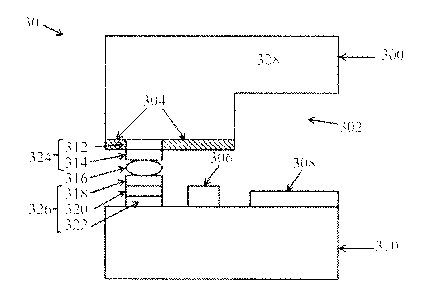
According to a further aspect, FIG. 3 is a block diagram of a side view of a
portion of
a packaged infrared detector similar to FIG. 1. The packaged infrared detector
30 includes a
lid seal structure 324 that is formed on the lid substrate 328 before
deposition of the
barrier/getter material 304. The barrier/getter material 304 may be deposited
around a
perimeter of the lid seal structure 324 and may extend to the edge of the
cavity 302. In the
alternative, the barrier/getter material 304 may not extend to the edge of the
cavity 302. The
barrier/getter material 304 may be deposited up to the very edge of the
perimeter of the seal
structure 324, or in some instances, may actually overlap a portion of the
perimeter of the seal
structure 324 by a small amount, to prevent contact of the bonding material
with the lid wafer
surface. This may be a preferred embodiment if the barrier/getter material 304
is positioned
under the seal (rather than metal layer 312) and has a porosity that may lead
to leakage under
the seal structure 324.
In another aspect, FIG. 4 shows a block diagram of a side view of a portion of
a
packaged infrared detector where a barrier layer 430 is deposited directly
onto the substrate.
As used herein, the term "barrier layer" refers to a material that prevents
the interaction of the
bonding material with the silicon surface. The barrier layer 430 may also
function as an
optical and/or thermal (e.g., infrared) blocking layer when deposited on a
surface of the lid
substrate 428. In certain instances where an optical shield positioned over
the reference
devices is constructed from the same metal stack as the lid seal structure
424, extruded
bonding material from the seal area may wet onto the optical shield and be
drawn out of the
bond line. If the barrier layer 430 is not wetted by the bonding material
(solder), surface
tension will keep the extruded solder in the vicinity of the bond line, and
the barrier layer 430
may allow for a smaller spacing between the detector seal structure 426 and
the reference
device 406. In certain instances, this may allow for smaller infrared detector
designs (e.g.,
smaller die sizes) which may increase the die count of the detector wafer 410.
In some
embodiments, the bather layer 430 may comprises titanium-tungsten (TiW), and
the TiW
may prevent the bonding material, such as solder (e.g., gold (80%)-tin (20%)),
from wetting.
TiW may also generally be opaque for purposes of blocking light and/or
incident radiation
(e.g., infrared radiation). This may allow the barrier layer 430 to shield the
reference devices
406 from light and/or incident radiation. In certain embodiments, the bather
layer 430 may
comprise TiW or any other suitable material that may block incident radiation
and may resist
bonding with a bonding agent.
In various aspects, a lid seal structure 424 may be deposited onto the barrier
layer
430. This configuration may allow the barrier layer 430 to comprise one of the
layers of the
11
CA 02916672 2015-12-22
WO 2015/006327
PCT/US2014/045756
lid seal structure 424. One or more layers of barrier/getter material 404 may
then be
deposited onto the barrier layer 430 and around a perimeter of the lid seal
structure 424.
In yet another aspect, FIG. 5 illustrates a block diagram of a portion of a
packaged
infrared detector 50 with a first layer of barrier/getter material 504a
deposited on the lid
substrate 528. The lid seal structure 524 is then formed on top of the first
layer of
barrier/getter material 504a. This step is followed by depositing a second
layer of
barrier/getter material 504b on the surface of the first layer of
barrier/getter material 504a and
around a perimeter of the lid seal structure 524. In this example, the first
layer of
barrier/getter material 504a may be included as one of the layers of the lid
seal ring 524 and
may contribute toward hermetic sealing of the device.
According to a further aspect, FIG. 6 is another example of a packaged device
that is
similar to FIG. 4 with the inclusion of a deposition of a barrier layer 630 on
the substrate, but
differs in that this step is subsequently followed by the deposition of at
least one layer of
barrier/getter material 604. Thus, the barrier/getter material 604 is
deposited directly onto the
barrier layer 630 before the formation of the lid seal structure 624. Both the
barrier layer 630
and the barrier/getter material 604 may contribute toward hermetically sealing
the device.
In accordance with yet another aspect, FIG. 7 illustrates a block diagram of a
packaged device that combines various elements of the structures depicted in
FIGS. 4 and 5.
In this embodiment, a barrier layer 730 is first deposited on the lid
substrate 728. This is
followed by the deposition of a first layer of barrier/getter material 704a.
The lid seal
structure 724 is then formed on the first layer of barrier/getter material
704a. A second layer
of barrier/getter material 704b may then be deposited on the surface of the
first layer of
barrier/getter material 704a and around a perimeter of the lid seal structure
724.
Thus far, several different embodiments and features have been presented.
Particular
embodiments may combine one or more of these features depending on operational
needs
and/or component limitations. This may allow for increased adaptability of the
packaged
infrared detector to the needs of various user environments. As recognized by
one skilled in
the art, some embodiments may include additional features. It should be noted
that while the
focus of the description has been based on infrared detectors, other devices
such as micro-
electro-mechanical systems (MEMS) devices, may comprise similar features
(e.g., the use of
a layer that is resistive to bonding with a bonding agent) that may benefit
from the methods
and systems described herein.
FIG. 8 is a flowchart illustrating two methods for performing certain
embodiments of
the invention. At step 810 a substrate is provided with a cavity. The term
"substrate" as used
12
CA 02916672 2015-12-22
WO 2015/006327
PCT/US2014/045756
herein, refers to a base or underlying material to which metals and/or
additional materials or
layers are deposited. Substrates include, but are not limited to, e.g.,
electronic substrates,
metal substrates, ceramic substrates, polymer substrates, and the like, or
combinations
thereof. Electronic substrates include, but are not limited to, e.g.,
semiconductors, chips,
wafers, and substrates comprised of silicon, and the like, or combinations
thereof. Suitable
substrates may be comprised substantially of a single or primary material or
alternatively of
two or more materials selected from, e.g., metals, ceramics, polymers, and the
like, or
combinations thereof. Ceramics may include, e.g., silicon carbide (SiC) and
tantalum nitride
(TaN), but are not limited to these specific materials. Polymers may include,
e.g.,
organosilane glass (OS G) , low-k dielectrics, siloxanes,
methylsilsesquioxanes, polysiloxanes,
and other polymers selected from major classes of inorganic, organic, and
hybrid polymers.
The structure and composition of the substrate is therefore not limited. For
example,
materials and layers of a substrate may be of any arrangement, order (e.g.,
sequential,
hierarchical, etc.), and/or pattern as suits the intended application, article
of manufacture, or
composition of matter. For example, semiconductor substrates may comprise
silicon, but
may comprise, e.g., sapphire in cases where radiation resistance is important,
such as in
military applications. The substrate may be any material capable of
functioning as a
supporting structure, including, but not limited to, the semiconductive
substrates described
above.
In accordance with one or more embodiments, the substrate may include at least
one
cavity. As used herein, the terms "cavity" and "recess" are used
interchangeably and are to
be given their broadest ordinary meaning, including but not limited to, a
space or hollow area
that is surrounded by something such as one or more layers or structures. In
certain
instances, the cavity may be described as a recess or depression within a
wafer material that
does not actually extend through the wafer. According to a further aspect, the
substrate may
have at least one cavity and a surface surrounding the at least one cavity.
In certain instances, the substrate may be a lid substrate. As used herein,
the terms
"lid substrate," "lid wafer" and "cap wafer" are used interchangeably and
refer to a wafer
comprising at least one recess that is suitable for use with a device wafer
comprising one or
more electronic devices, such as MEMS devices. The cavity may include one or
more layers
of an optically transmissive material. In such a configuration, the lid wafer
provides an
optically transmissive window above the MEMS devices. The lid substrate may be
a
thermally and/or optically transparent silicon wafer. In some embodiments, the
lid substrate
may comprise materials other than silicon.
13
CA 02916672 2015-12-22
WO 2015/006327
PCT/US2014/045756
According to one or more embodiments, at step 820a a seal structure may be
formed
on a portion of the substrate, or in the alternative, at step 830b, the seal
structure may be
formed on a portion of the barrier/getter material. For example, the seal
structure may form a
ring around a perimeter of the at least one cavity. The term "seal structure"
is intended to
mean one or more structures that can be used to form at least part of a seal
for one or more
electronic devices within an electrically active area of a substrate from
ambient conditions.
In various aspects, the seal structure may be used in conjunction with a
substrate that includes
one or more electronic components to form an encapsulation assembly. The
encapsulation
assembly may function to substantially protect a portion or portions of the
electronic
component(s) from damage originating from a source external to the electronic
device. In
some embodiments, a lid, by itself, or in combination with one or more other
objects, may
form an encapsulation assembly. The encapsulation assembly may function as a
hermetically
sealed package.
The seal structure, such as the lid seal structure formed at step 820a, may
comprise a
stack of metal that includes Ti or TiW, nickel, and gold. In some embodiments,
such as in
the combination of steps 820b and 830b, the bottom layer of the seal structure
stack may
comprise the barrier/getter material. For example, if the barrier/getter
material is titanium,
the bottom layer of the lid seal structure may be titanium and the rest of the
stack may include
nickel and gold. Each lid seal structure may surround, but be slightly larger
than, a cavity in
the lid substrate and any window formed in the barrier/getter material. The
shape of the lid
seal structure may correspond to the shape and size of any detector seal
structure formed on a
corresponding detector wafer. For example, a seal structure on the surface of
the substrate
may form a ring around a perimeter of a cavity.
In various embodiments at least one layer of barrier/getter material, such as
titanium,
may be deposited on a surface of a lid substrate at step 820b. In the
alternative, the
barrier/getter material may be deposited on the surface of the lid substrate
to form a ring
around a perimeter of the seal structure, as indicated at step 830a. The
barrier/getter material
may be deposited on an entire surface of the substrate, or may be deposited on
one or more
portions of the substrate, for example, through the use of a shadow mask. In
certain aspects,
the barrier/getter material may be titanium, including pure titanium.
According to one or
more embodiments, the titanium material may have a thickness in a range of
about 1000
Angstroms to about 10,000 Angstroms. According to other embodiments, the
titanium
material may have a thickness greater than 10,000 Angstroms. The thickness of
the titanium
material may be any thickness that is suitable for the purposes of function as
a getter for a
14
CA 02916672 2015-12-22
WO 2015/006327
PCT/US2014/045756
specific application or device. The barrier/getter material may be configured
to block light
and/or incident radiation to one or more reference devices. In addition, the
barrier/getter
material may be resistive to bonding with a bonding agent used to form a
complete electronic
device.
As used herein, the term "layer" is used interchangeably with the term "film"
and
refers to a coating covering a desired area. The term is not limited by size.
Layers and films
can be formed by any deposition technique, including vapor deposition, liquid
deposition,
and thermal transfer.
According to at least one aspect, vacuum evaporation or sputtering methods may
be
used for purposes of depositing the at least one layer of titanium material.
For example, in
certain embodiments, titanium material may be deposited under high vacuum
conditions in
the absence of reactive gases. In one or more aspects, it may be necessary to
remove any
native oxides present on the substrate surface before depositing the titanium
material.
Suitable reaction conditions, including reaction atmosphere, reaction
temperature, duration of
the reaction, and workup procedures may each be chosen based on a specific
application, as
recognized by one skilled in the relevant technology. In various aspects, the
deposition
process results in a titanium material that is highly porous, with a maximum
surface area and
microstructure, i.e., numerous boundaries between the various grains or
crystalline structures
that constitute the layer.
In various aspects, the at least one layer of titanium material may be
characterized as
porous. In one or more aspects, the titanium material may be characterized as
being more
porous than one or more other materials used in the device. For example, the
titanium
material may be more porous than an underlying barrier layer. The titanium
material may be
porous for purposes of functioning as a getter. In some instances, the
titanium material may
have a porosity that may contribute toward leakage if it is positioned in
between the silicon
substrate of the lid wafer and one or more components of the lid seal
structure. In such
instances, it may be beneficial to position a layer of barrier material (with
a porosity that is
lower than the titanium material) directly on the lid substrate to function as
a barrier between
the layer of titanium and the one or more components of the lid seal
structure.
Referring back to FIG. 8, in certain embodiments at step 840 the
barrier/getter
material may be activated. As used herein, the term "activating," when used in
reference to
titanium material, refers to any process that may be performed on the titanium
material that
allows it to function as a getter material. For example, in certain
embodiments, the titanium
material may be activated by subjecting the device package to a suitable
combination of
CA 02916672 2015-12-22
WO 2015/006327
PCT/US2014/045756
temperature and time. According to certain aspects, activation may occur when
device
fabrication is complete. In some embodiments, the device package may be
hermetically
sealed when the barrier/getter material is activated. In other embodiments,
the titanium
material may be activated during the hermetic sealing process, i.e., bonding
or aligning the lid
wafer to the device wafer. In certain non-limiting embodiments, the titanium
material may be
activated by placing the material in a vacuum environment and heating it to a
temperature in
a range of about 200 C to about 500 C for a period of time in a range of
about 10 minutes to
about 120 minutes. The process involved for activation of the at least one
layer of titanium
material may be performed under any conditions suitable for causing desorption
of any
unwanted species in the titanium material and allowing the titanium material
to function as a
getter and as a barrier as described herein. In some aspects, the titanium
material may
function as a barrier layer even without the occurrence of activation. In
other aspects, the
titanium material may function as an optical shield. This functionality may
exist either with
or without activation. In various aspects, activating results in a
barrier/getter material
possessing at least one of high porosity, low particulating, and mechanically
strong structure.
In various aspects, subsequent processing may be configured to preserve the
functionality of the barrier/getter material after activation, for example, so
that an exposed
surface of the barrier/getter material is still able to react or absorb one or
more gas species
and thereby function as a getter material. According to certain aspects,
specific temperatures
and materials used in later processing steps may be specifically chosen to
preserve the
integrity of the barrier/getter material to function as a getter material.
This may include
avoiding the use of one or more chemicals (i.e., reactive acids) or
environments that may
react with the barrier/getter material. For example, after activation the
barrier/getter material
may only be exposed to vacuum or otherwise oxygen-free environments.
FIG. 9 also illustrates two methods for performing certain embodiments of the
invention, and is similar to the method outlined in FIG. 8, with the exception
that the
substrate is not provided with a cavity. At step 910 a substrate, such as a
lid substrate, is
provided. In step 910a, a seal structure may be formed on the substrate, or,
in the alternative,
the seal structure may be formed after the deposition of barrier/getter
material (step 920b) at
step 930b. In step 920b, barrier/getter material may be deposited on the lid
substrate, or, in
the alternative, the barrier/getter material may be deposited on the surface
of the lid substrate
to form a ring around a perimeter of the seal structure, as indicated at step
930a.
At step 940, one or more cavities may be formed by removing portions of the
lid
substrate and/or barrier/getter material. For example, at least one layer of
barrier/getter
16
CA 02916672 2015-12-22
WO 2015/006327
PCT/US2014/045756
material, such as titanium material, may be deposited on a substrate and
subsequently the at
least one layer of titanium material and the substrate may undergo an etching
process wherein
a cavity is formed in the substrate. In other instances, lid seal rings may be
deposited either
before or after the deposition of the barrier/getter material, and the cavity
may then be formed
thereafter. In various embodiments, a cavity or other features to be created
on a substrate
may be formed by using photolithography techniques. For example, a photoresist
mask may
applied to the at least one layer of barrier/getter material to define a
pattern, such as a cavity,
that is to be etched into the substrate and the barrier/getter material. In a
further example, the
pattern may include a plurality of windows in the barrier/getter material and
a plurality of
cavities in the lid substrate. The number of windows and cavities may
correspond to the
number of detector arrays, and both the windows in the barrier/getter material
and the cavities
in the lid substrate may be formed from the same photoresist mask. This may
help to ensure
that at least two of the dimensions of both a window in the barrier/getter
material and the
cavity in the lid substrate are substantially similar and that the
barrier/getter material extends
right up to the edge of the cavity in the lid substrate. The use of the same
mask may also
reduce the number of steps needed to manufacture the packaged infrared
detector.
The cavity may be formed by removing a portion of the barrier/getter material,
a
portion of the lid substrate, or both. One or more processes, as recognized by
one skilled in
the art, may be used to form the cavity, such as, for example, an etch
process. In certain
instances, the cavity may extend through a portion of the total thickness of
the lid substrate
and leave at least some of the lid substrate to cover a detector device.
Activation of the
barrier/getter material may occur at step 950, after the formation of the
cavity, as described
above.
Some of the steps illustrated in FIGS. 8 and 9 may be combined, modified or
deleted
where appropriate, and additional steps may also be added to the process flow.
Additionally,
steps may be performed in any suitable order without departing from the scope
of particular
embodiments. The steps depicted in FIGS. 8 and 9 are just examples of the
steps performed
for particular embodiments, and other embodiments may use different steps
arranged in a
different order. For example, in some embodiments, the cavity may be formed in
the lid
substrate after the deposition of both a barrier layer and a layer of
barrier/getter material on
the surface of the lid substrate. Furthermore, seal structures may be formed
on the
combination of the barrier layer and a layer of barrier/getter material, or
the seal structures
may be formed on the barrier layer with the layer of barrier/getter material
forming a ring
17
CA 02916672 2015-12-22
WO 2015/006327
PCT/US2014/045756
around a perimeter of the seal structures. The cavity may be subsequently
formed in the lid
substrate.
According to one or more embodiments, a method of fabricating an electronic
device
may include depositing at least one barrier layer on the surface of the
substrate. In certain
non-limiting embodiments, the at least one barrier layer may be titanium-
tungsten. In certain
embodiments, the bather layer may not bond with a bonding agent used, for
example, to seal
a lid wafer to a detector wafer. In various embodiments, the barrier layer may
function to
shield one or more reference devices from incident radiation being detected by
one or more
detector devices. In other instances, the barrier layer may function to shield
the barrier/getter
material from contamination, such as from contamination or unwanted species in
the
underlying substrate.
In various embodiments, a method for fabricating an electronic device may
further
comprise aligning a first seal structure on a first substrate to a second seal
structure on a
second substrate. In certain aspects the first substrate may include a lid
wafer and the second
substrate may be a device wafer. The alignment may be performed so that at
least one cavity
formed on the first substrate may configure to at least one detector device
formed on the
second substrate. As used herein, the term "configure," when used in reference
to alignment,
refers to positioning one or more features or elements of a first substrate in
a position in
reference to one or more features or elements of a second substrate so that
the one or more
features are allowed to function properly. For example, the cavity on the
first substrate may
be configured so that a perimeter surrounding the cavity may be positioned
over and around a
perimeter of the detector device. Such an arrangement allows light penetrating
the cavity to
be detected by the detector device. In a further example, the detector seal
structures may be
aligned with the lid seal structures. In various embodiments, aligning the
detector seal
structure and the lid seal structure may allow windows in the barrier/getter
material and
cavities in the lid substrate to be aligned with the detector device. This may
allow for a
thermally and/or optically transmissive window to cover the detector device.
Such an
arrangement may provide protection for the detector device while still
allowing light and/or
incident radiation to reach the detector device. Furthermore, because the
barrier/getter
material may cover the lid wafer, except for the cavity portions, the
barrier/getter material
may block a portion of light and/or incident radiation from reaching the
reference device.
According to certain embodiments, the method of fabricating an electronic
device
may further comprise bonding the first substrate to the second substrate. As
used herein, the
term "bonding" may be used interchangeably with the term "sealing" and is
intended to mean
18
CA 02916672 2015-12-22
WO 2015/006327
PCT/US2014/045756
to permanently affix one surface to another. Bonding may include applying a
bonding agent
to a lid seal structure, a detector seal structure, or both. The bonding agent
may be any type
of bonding material that may be used to seal the detector wafer to the lid
wafer. For example,
the bonding agent may be solder, such as gold-tin solder (e.g., gold (80%)-tin
(20%) solder).
In certain embodiments, the bonding agent may be such that it adheres to the
detector seal
structure and lid seal structure, but does not adhere to or bond with the
barrier/getter material.
For example, in the case of solder, the bonding agent may readily wet to a
detector seal
structure and a lid seal structure, but may not wet to the barrier/getter
material. Furthermore,
in instances where a barrier material is used, the barrier material may be
resistant to bonding
with a bonding agent. For example, the barrier material may be a metal such as
titanium,
titanium-tungsten or titanium nitride, to which melted solder does not wet.
Bonding the lid wafer to the detector wafer may create a sealed volume within
which
the detector device is sealed. In some embodiments in which solder is used as
the bonding
agent, bonding a lid wafer to a detector wafer may comprise melting the solder
so that it is in
a liquid state. In the liquid state, the solder may spread onto the
barrier/getter material.
However, because the barrier/getter material does not bond with the bonding
agent (e.g., the
solder may not readily wet to the barrier/getter material), as the solder
begins to cool, it may
draw back within the seal structure and thereby decrease, or eliminate, the
spread of solder
beyond the seal structure. This may allow the seal structure to be closer to
the reference
detector arrays and/or the detector arrays.
Although particular embodiments have been described in detail, it should be
understood that various other changes, substitutions, combinations, and
alterations may be
made hereto without departing from the spirit and scope of the disclosure. It
is intended that
particular embodiments encompass all such changes, substitutions, variations,
alterations, and
modifications as falling within the spirit and scope of the appended claims.
For example,
although an embodiment has been described with reference to a number of
elements included
in a packaged infrared detector, such as cavities, detector devices, reference
devices, seal
structures, barrier layers, barrier/getter material, and bonding agents, these
elements may be
combined, rearranged, modified or re-positioned in order to accommodate
particular
detection or manufacturing needs. In addition, any of these elements may be
provided as
integrated internal or separate external components to each other where
appropriate.
Particular embodiments contemplate great flexibility in the arrangement of
these elements as
well as their internal components.
19