Note: Descriptions are shown in the official language in which they were submitted.
CA 02918695 2016-01-19
WO 2015/007330 1
PCT/EP2013/065255
Methods and devices for power compensation
Technical field
The technology disclosed herein relates generally to the field of electrical
power
systems, and in particular to reactive power compensation within such systems.
Background
Reactive power compensators are used for voltage control, reactive/active
power flow
control, transient and steady-state stabilization for improving the operation
and
functionality of e.g. electrical power transmission and distribution systems.
Thyristor Controlled Reactors (TCRs)/Thyristor Switched Reactors (TSRs) and
Thyristor Switched Capacitors (TSCs) have been widely used as inductive and
capacitive reactive power branches of Static Var Compensators (SVCs),
respectively.
A drawback of the TCR is the amount of harmonics, e.g. 5th, 7th, 11th, r-th
3 ,..,etc.
harmonics, that it generates during steady state operation and also, during
unbalanced network voltage, harmonics of 3rd, 9th,,, .etc. order. For the TCR,
harmonic filter branches are normally required in order to reduce the harmonic
emission to reach performance levels specified by the network operator. Such
filter
branches are expensive and require large footprint, e.g. in a substation where
they are
typically placed.
The TSR does not generate low order harmonics, but a drawback of the TSR is
that it
creates large current transients in the feeding network when switched in or
out,
causing voltage disturbances. In order to minimize the voltage transients from
the
TSR, it is often necessary to divide the TSR in smaller sizes and/or use it
together
with TSC.
The TSC comprises capacitor banks requiring large footprint, and energizing
transients of the capacitor banks have to be taken care of. In particular,
energizing a
second capacitor bank when a first capacitor bank is already energized, i.e.
back-to-
back switching, requires the frequency and amplitude of voltage oscillations
on a
busbar to be limited in order not to generate overvoltages.
Nowadays, it is a trend to replace these branches by Voltage Source Converter
(VSC)
based chain-link technology. The chain-link technology of the VSC is however
rather
CA 02918695 2016-01-19
WO 2015/007330 2
PCT/EP2013/065255
costly to implement, mainly since it entails advanced power electronics
switching
devices and advanced control technology.
The various power compensation devices thus have their advantages as well as
drawbacks and while high performance can be obtained, it comes with high
costs,
both initial costs and maintenance costs.
Summary
An object of the present teachings is to address the above by providing a
power
compensation arrangement having balanced cost versus performance.
The object is according to a first aspect achieved by a method performed in a
control
device for controlling a power compensation arrangement comprising a voltage
source converter and one or more power compensation branches. Each power
compensation branch comprises a thyristor controlled reactor, a thyristor
switched
reactor or a thyristor controlled capacitor. The voltage source and the one or
more
power compensation branches are connected to a same busbar. The method
comprises: detecting a request in an electrical power system to which the
power
compensation arrangement is connected; determining, based on the request, a
need
for reactive power supply to the electrical power system; providing reactive
power by
means of the voltage source converter and/or by one or more of the power
compensation branches; and compensating, by means of the voltage source
converter, any disturbances caused by the power compensation branches when
providing the reactive power to the electrical power system.
The method for controlling the power compensation arrangement provides the
benefits of the voltage source converter, while enabling reduced costs by also
taking
advantage of the less expensive thyristor controlled reactors, thyristor
switched
reactors and/or thyristor switched capacitors.
The object is according to a second aspect achieved by a control device for
controlling
a power compensation arrangement. The power compensation arrangement
comprises a voltage source converter and one or more power compensation
branches,
each power compensation branch comprising a thyristor controlled reactor, a
thyristor switched reactor or a thyristor controlled capacitor. The voltage
source
converter and the one or more power compensation branches are connected to a
CA 02918695 2016-01-19
WO 2015/007330 3
PCT/EP2013/065255
same busbar. The control device is configured to: detect a request in an
electrical
power system to which the power compensation arrangement is connected;
determine, based on the request, a need for reactive power supply to the
electrical
power system; provide reactive power by means of the voltage source converter
and/or by one or more of the power compensation branches; and compensate, by
means of the voltage source converter, any disturbances caused by the power
compensation branches when providing the reactive power to the electrical
power
system.
Advantages corresponding to the above are obtained also by the control device.
The object is according to a third aspect achieved by a computer program for a
control device configured to control a power compensation arrangement
comprising
a voltage source converter and one or more power compensation branches,
wherein
each power compensation branch comprising a thyristor controlled reactor, a
thyristor switched reactor or a thyristor controlled capacitor. The voltage
source
is converter and the one or more power compensation branches are connected
to a
same busbar. The computer program comprises computer program code, which,
when run on the control device causes the control device to: detect a request
in an
electrical power system to which the power compensation arrangement is
connected;
determine, based on the request, a need for reactive power supply to the
electrical
power system; provide reactive power by means of the voltage source converter
and/or by one or more of the power compensation branches; and compensate, by
means of the voltage source converter, any disturbances caused by the power
compensation branches when providing the reactive power to the electrical
power
system.
Advantages corresponding to the above are obtained also by the computer
program.
The object is according to a fourth aspect achieved by a computer program
product
comprising a computer program as above, and a computer readable means on which
the computer program is stored.
Advantages corresponding to the above are obtained also by the computer
program
product.
CA 02918695 2016-08-16
= 3a
According to another aspect of the present invention, there is provided a
method
performed in a control device for controlling a power compensation arrangement
comprising a voltage source converter and at least one power compensation
branch,
each power compensation branch comprising a thyristor controlled reactor, a
thyristor switched reactor or a thyristor controlled capacitor, the voltage
source
converter and the at least one power compensation branch being connected to a
same busbar, the method comprising:
- detecting a request in an electrical power system to which the power
compensation
arrangement is connected;
- determining, based on the request, a need for reactive power supply to
the
electrical power system to be larger than a reactive power capacity of the
voltage
source converter or determined to minimize total losses of the power
compensation
arrangement;
- providing reactive power by means of the voltage source converter and by at
least
one of the power compensation branches; and
- compensating, by means of the voltage source converter, any disturbances
caused
by the power compensation branches when providing the reactive power to the
electrical power system,
- wherein the providing of reactive power comprises a sub-step of determining
availability of the at least one power compensation branch and providing the
reactive power based on the determination.
According to another aspect of the present invention, there is provided a
control
device for controlling a power compensation arrangement comprising a voltage
source converter and at least one power compensation branch, each power
compensation branch comprising a thyristor controlled reactor, a thyristor
switched
reactor or a thyristor controlled capacitor, the voltage source converter and
the at
least one power compensation branch being connected to a same busbar, the
control
device being configured to:
CA 02918695 2016-08-16
3b
- detect a request in an electrical power system to which the power
compensation
arrangement is connected;
- determine, based on the request, a need for reactive power supply to the
electrical
power system to be larger than a reactive power capacity of the voltage source
converter or determined to minimize total losses of the power compensation
arrangement;
- provide reactive power by means of the voltage source converter and by at
least
one of the power compensation branches; and
- compensate, by means of the voltage source converter, any disturbances
caused by
the at least one power compensation branch when providing the reactive power
to
the electrical power system,
- wherein the providing of reactive power comprises a sub-step of determining
availability of the at least one power compensation branch and providing the
reactive power based on the determination.
According to another aspect of the present invention, there is provided a
computer
program product comprising a computer readable means on which is stored a
computer program for a control device configured to control a power
compensation
arrangement comprising a voltage source converter and at least one power
compensation branch, each power compensation branch comprising a thyristor
controlled reactor, a thyristor switched reactor or a thyristor controlled
capacitor,
the voltage source converter and the at least one power compensation branch
being
connected to a same busbar, the computer program comprising computer program
code, which, when run on the control device causes the control device to:
- detect a request in an electrical power system to which the power
compensation
arrangement is connected;
- determine, based on the request, a need for reactive power supply to the
electrical
power system to be larger than a reactive power capacity of the voltage source
converter or determined to minimize total losses of the power compensation
arrangement;
CA 02918695 2016-08-16
3c
- provide reactive power by means of the voltage source converter and by at
least
one of the power compensation branches; and
- compensate, by means of the voltage source converter, any disturbances
caused by
the at least one power compensation branch when providing the reactive power
to
the electrical power system,
- wherein the providing of reactive power comprises a sub-step of determining
availability of the at least one power compensation branch and providing the
reactive power based on the determination.
CA 02918695 2016-01-19
WO 2015/007330 4
PCT/EP2013/065255
Further features and advantages of the present teachings will become clear
upon
reading the following description and the accompanying drawings.
Brief description of the drawings
Figure 1 illustrates an embodiment of a power compensation arrangement
according
to the present teachings.
Figure 2 illustrates another embodiment of a power compensation arrangement
according to the present teachings.
Figure 3 is a flow chart over steps of a method according to the present
teachings.
Figure 4 illustrates a control device according to the present teachings.
Detailed description
In the following description, for purposes of explanation and not limitation,
specific
details are set forth such as particular architectures, interfaces,
techniques, etc. in
order to provide a thorough understanding. In other instances, detailed
descriptions
of well-known devices, circuits, and methods are omitted so as not to obscure
the
description with unnecessary detail. Same reference numerals refer to same or
similar elements throughout the description.
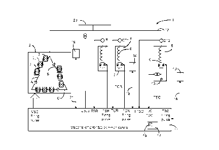
Figure 1 illustrates an embodiment of a power compensation arrangement
according
to the present teachings. The power compensation arrangement 1 comprises a
voltage
source converter 2 (VSC) based on chain-link technology. A three-phase chain-
link
converter comprises three phase legs, where each phase leg comprises a number
of
series-connected chain-link modules. The VSC 2 comprises three such phase-legs
A,
B, C, each phase leg thus comprising a number of series-connected chain-link
modules, in the following denoted converter cells, e.g. converter cells 31,
32,..., 3n of
phase leg A. Such converter cells 31, 32,..., 3n are also denoted switching
cells and the
particular layout of the converter cells is not important for the present
teachings. For
example, each converter cell 31, 32,..., 3n may comprise four valves connected
in an H-
bridge arrangement with a capacitor unit (often denoted full-bridge converter
cell).
Each valve in turn may comprise a transistor switch, such as an IGBT
(Insulated Gate
Bipolar Transistor), having a free-wheeling diode connected in parallel
thereto. It is
noted that other semiconductor devices could be used, e.g. gate turn-off
thyristors
CA 02918695 2016-01-19
WO 2015/007330 5
PCT/EP2013/065255
(GTO) or Integrated Gate-Commutated Thyristors (IGCT). The converter cells 31,
32,..., 3n could alternatively comprise half-bridge converter cells, and it is
noted that
yet other converter topologies could benefit from the present teachings. The
other
phase legs B, C also comprise such series-connected converter cells.
In the figure, the phase legs A, B, C comprising the series-connected
converter cells
are connected in a delta configuration. In other embodiment, the phase legs
are
connected in a wye-configuration.
In the embodiment illustrated in figure 1, the power compensation arrangement
1
further comprises three other power compensating branches. In particular, the
power
compensation arrangement 1 comprises a first branch comprising a thyristor
controller reactor (TCR) 4, a second branch comprising a thyristor switched
reactor
(TSR) 8 and a third branch comprising a thyristor switched capacitor (TSC) 5.
Both a TCR and a TSR comprises, for each phase, a thyristor 7 controlled
inductor 6.
A difference between a TCR and a TSR is that the reactance of the TCR can be
varied
in a continuous manner by partial-conduction control of the thyristor 7 value,
while
the reactance of the TSR can be varied in a step-wise manner by full- or zero
conduction operation of the thyristor value.
As was mentioned in the background section, a TCR typically require a filter
device
for handling harmonics. For example, a filter circuit comprising capacitor and
series
reactance, tuned to a particular harmonic frequency, which is to be filtered
out. It is
noted that in accordance with the present teachings, such filter device may be
omitted by instead handling the harmonics created when switching in the TCR 4
by
the VSC 2, as will be described later.
The TSC 5 comprises a thyristor 9 switched capacitor 10, which may comprise a
single capacitor, but typically comprises a bank of capacitors. The reactance
of the
TSC 5 can be varied in a stepwise manner by full- or zero conduction operation
of the
thyristor value.
The power compensation arrangement 1 may be connected to an electrical power
system or electrical power network or to an electrical load, e.g. an
industrial load.
Such electrical power system is schematically indicated at reference numeral
20, and
it is noted that various devices (not illustrated), such as transformers, are
typically
CA 02918695 2016-01-19
WO 2015/007330 6
PCT/EP2013/065255
placed between the power compensation arrangement 1 and the electrical power
system 20 to which it is to be connected.
The VSC 2 and the one or more branches of the power compensation arrangement
1,
i.e. the one or more branches comprising a TCR 4, one or more branches
comprising
a TSR 8 and the one or more branches comprising a TSC 5 are connected to a
common busbar 12.
The power compensation arrangement 1 of the present teachings may be adapted
in
dependence on the needs of the particular application at hand. In particular,
the
power compensation arrangement 1 comprises the VSC 2 and one or more of power
compensation branches 4, 5, 8. Each of the power compensation branches 4, 5, 8
may
comprises a TCR 4, TSR 8 and/or a TSC 5, and all power compensation branches
4, 5,
8 are connected to the one and same bus bar 12. In one embodiment thus (not
illustrated), the power compensation arrangement 1 comprises the VSC 2 and the
TCR 4. In another embodiment (not illustrated), the power compensation
arrangement 1 comprises the VSC 2 and the TSC 5. In yet another embodiment
(not
illustrated), the power compensation arrangement 1 comprises the VSC 2 and the
TSR 8. In still other embodiments, the power compensation arrangement 1
comprises
the VSC 2 and two or more branches of TCR 4 and/or TSR 8, and/or two or more
branches of TSC 5. Figure 2 exemplifies one of the various possible
embodiments of a
power compensation arrangement 1 according to the present teachings. In
particular,
the power compensation arrangement 1 of figure 2 comprises the VSC 2, the TCR
4
and two branches of TSC 5: TSC 5, and TSC 52. The teachings of the present
application thus encompass any combination of VSC 2 and one or more of TCR 4,
TSR 8 and TSC 5.
The power compensation arrangement 1 is controlled by a common control system,
which common control system is used to control the TCR 4, the TSR 8, the TSC 5
and
the VSC 2. In particular, in an embodiment a control device 11 is configured
to control
all the branches 4, 5, 8 of the power compensation arrangement 1. In other
embodiments, several control devices 11, 13, 14 are utilized. The control
device 11 may
comprise a processor using any combination of one or more of a suitable
central
processing unit (CPU), multiprocessor, microcontroller, digital signal
processor
(DSP), application specific integrated circuit etc., capable of executing
software
CA 02918695 2016-01-19
WO 2015/007330 7
PCT/EP2013/065255
instructions stored in a memory 17, which can thus be a computer program
product.
The control device 11 can be configured to execute various embodiments of a
method,
to be described next, for controlling the power compensation arrangement 1.
Figure 3 is a flow chart over steps of a method according to the present
teachings. The
method 30 may be performed in a control device 11 for controlling a power
compensation arrangement 1 as described. In particular, for controlling a
power
compensation arrangement 1 comprising a voltage source converter 2 and one or
more power compensation branches 4, 5, 8, wherein each power compensation
branch 4, 5, 8 comprises a thyristor controlled reactor, a thyristor switched
reactor or
a thyristor controlled capacitor. The voltage source converter 2 and the one
or more
power compensation branches 4, 5, 8 are connected to a same busbar 12.
The method 30 comprises detecting 31 a request in an electrical power system
20 to
which the power compensation arrangement 1 is connected. The power
compensation
arrangement 1 is typically connected to an electrical power network 20 in
order to
handle unbalanced network conditions occurring in the electrical power network
20.
The request may for example comprise a fault condition, a request from a
voltage
control, a request from a reactive power control, a request from an operator
of the
electrical power system or a request based on changes in the electrical power
system.
The detecting 31 of a request, when it comprises a fault condition, may be
done in any
conventional manner, for example by measuring certain voltages and/or
currents,
comparing them to desired values (target values) and when detecting a
deviating
measured value a fault condition is detected.
When the request comprises a request from a control device, such as a voltage
control
or a reactive power control, the detecting 31 of a request may then comprise
detecting
a signal indicating a system voltage condition not being equal to a reference
value.
The change in reactive power output of the power compensation arrangement 1
may
thus be ordered e.g. by a voltage control device to maintain the electrical
power
system voltage at a reference value. Correspondingly, when the request
comprises a
request from the operator of the electrical power system, or when it is based
on
changes in the electrical power system, the detecting of the request may then
comprise receiving a signal indicating such respective request. For example,
an
operator may enter a request to increase/decrease the reactive power out of
the
CA 02918695 2016-01-19
WO 2015/007330 8
PCT/EP2013/065255
power compensation arrangement 1 e.g. by means of a keyboard, and the control
device 11 may thus receive a corresponding signal and effectuate the request
by the
operator.
The method 30 further comprises determining 32, based on the request, a need
for
reactive power supply to the electrical power system 20. The determining 32 a
need
for reactive power can also be done in any conventional manner, e.g. by
detecting a
fault condition and calculating amount of reactive power supply needed to
remove
the fault condition.
The method 30 further comprises providing 33 reactive power by means of the
voltage source converter 2 and/or by one or more of the power compensation
branches 4, 5, 8. In some cases only the voltage source converter 2 is needed
as power
compensation source, and in some cases additional power compensation may be
required, e.g. if the capacity limit of the VSC 2 has been reached. In an
embodiment,
in case the VSC 2 is unable to provide the reactive power needed, then one or
more of
the power compensation branches 4, 5, 8 is switched in, providing the
additional
reactive power that is needed. In other cases, additional power compensation
may be
required in order to minimize the losses of the power compensation arrangement
1.
That is, the power compensation branches 4, 5, 8 may be switched in or out
when the
voltage source converter 2 reaches its limits or they can be switched in or
out in order
to minimize losses of the power compensation arrangement 1.
The method 30 further comprises compensating 34, by means of the voltage
source
converter 2, any disturbances caused by the power compensation branches 4, 5,
8
when providing the reactive power to the electrical power system 20. The VSC 2
is
thus used for compensating for any disturbances, e.g. harmonics or current
transients
that may occur when switching in one of the power compensation branches 4, 5,
8.
In an embodiment thus, the determining 32 the need for reactive power supply
to the
electrical power system 20 is determined to be larger than a reactive power
capacity
of the voltage source converter 2. That is, the reactive power need of the
electrical
power system 20 is larger than what the VSC 2 is able to provide. The
providing 33 of
reactive power then comprises using one or more of the power compensation
branches 4, 5, 8 in addition to the voltage source converter 2.
CA 02918695 2016-01-19
WO 2015/007330 9
PCT/EP2013/065255
In an embodiment, the power compensation branch comprises a thyristor
controlled
reactor 4 and the compensating 34 of disturbances comprises:
- measuring a current ITcR from the thyristor controlled reactor 4, and
- compensating, based on the measured current ITCR, harmonics caused by the
thyristor controlled reactor 4.
The TCR 4 current ITcR (see figure 1) may be measured by means of e.g. a
current
transformer CTi (see figure 1) or by means of a transducer. The current
response may
then be used so as to control the VSC 2 to compensate for harmonics generated
by the
TCR 4. When the electrical power network 20 shows unbalanced network
conditions,
the TCR 4 current unbalance and corresponding uncharacteristic harmonics may
also
be compensated for by the VSC 2.
In an embodiment, the power compensation branch comprises a thyristor switched
reactor 8 and the compensating 34 of disturbances comprises:
- measuring a current 'TSR from the thyristor switched reactor 8, and
- compensating, based on the measured current 'TSR, current transients caused
by the
thyristor switched reactor 8.
When switching the TSR 8 in and out, the TSR 8 current 'TSR (see figure 1)
comprises
a positive-sequence component and a negative-sequence component, causing
voltage
steps and voltage unbalance in the electrical power network 20. In such case,
the
measured TSR 8 current 'TSR may be used as reference current to the control
device ii
so as to minimize current transients.
In an embodiment, the power compensation branch comprises a thyristor switched
capacitor 5 and the compensating 34 of disturbances comprises:
- measuring a current ITSC and voltage UC_TSC of the thyristor switched
capacitor 5,
and a bus 12 voltage Ubus,
- predicting a thyristor switched capacitor 5 current, based on the
measured current
ITSC and voltages UC_TSC, Ubus, and based on a switching time instance giving
a
minimal voltage UC_TSC of the thyristor switched capacitor 5, and
CA 02918695 2016-01-19
WO 2015/007330 10
PCT/EP2013/065255
- compensating, based on the predicted thyristor switched capacitor 5 current,
for the
sum of transient currents of the thyristor switched capacitor 5 and the
voltage source
converter 2.
For the case of the power compensation arrangement 1 comprising the TSC 5, the
TSC 5 current ITsc (see figure 1), the TSC capacitor voltage UC_TSC (see
figure 1) and
the bus voltage Ubus (see figure 1) may be measured in order to predict the
TSC 4
current when switched in. The predicted current is then used by the control
device ii
so as to control the VSC 2 to minimize the transient current summation of the
TSC 5
and VSC 2, thus reducing the disturbance to the electrical power network 20
caused
by switching in the thyrsitor switched capacitor 5.
In an embodiment, the providing 32 of reactive power comprises a sub-step of
determining availability of the power compensation branches 4, 5, 8 and
providing
the reactive power based on the determination. Certain power compensation
branches may for example be unavailable, and the determination may be done by
identifying if there are any switches (e.g. circuit breakers) open, which
would identify
the corresponding power compensation branch to be unavailable.
As mentioned earlier, a common control system is provided controlling the
power
compensation arrangement 1. The common control system may comprise the control
device 11 or a combination of the control device ii and additional control
devices, e.g.
control devices 13, 14 and 19, wherein each additional control device is
configured to
control a respective branch, or several branches. In a particular embodiment,
illustrated in figure 1, the common control system comprises the control
device ii and
a second control device 13, a third control device 14 and a fourth control
device 19.
The second control device 13, the third control device 14 and the fourth
control device
19 have communication means 15, 16, and 21 respectively, to communicate
control
signaling to the control device ii and receive control signaling from the
control device
ii. The communication means 15, 16, 21 may comprise wired or wireless
communication means, such as for example fiber optic cables or Ethernet. The
second control device 13 is configured to provide signaling, e.g. control
signals, to the
control device ii that relates to the branch to which it is related, i.e. the
branch
comprising the TCR 4. The third control device 14 is configured to provide
signaling,
e.g. control signals, to the control device ii that relates to the branch to
which it is
CA 02918695 2016-01-19
WO 2015/007330 11
PCT/EP2013/065255
related, i.e. the branch comprising the TSC 5. The fourth control device 19 is
configured to provide signaling, e.g. control signals, to the control device
ii that
relates to the branch to which it is related, i.e. the branch comprising the
TSR 8.
Figure 4 illustrates a control device ii according to the present teachings.
The control
device ii (refer also to figure 1) comprises an input/output (I/O) device 23
for
receiving e.g. control signaling from the second, third and fourth control
devices 13,
14, 19, and measurement values for measurements made in e.g. one of the power
compensation branches (if such values are not conveyed via the respective
control
device) or measurements made in the electrical power system 20 to which the
power
compensation arrangement 1 is connected. It is noted that although the I/O
device 23
is illustrated as a single device, it could comprise several devices. The
control device
ii further comprises one or more processor circuits 22 and memory 17. The
memory
17 contains instructions executable by the processor circuits 22, whereby the
control
device 11 is operative to perform any of the embodiments of the method 30 as
described.
The control device 11 is thus configured to control a power compensation
arrangement 1 as has been described. In particular, a power compensation
arrangement 1 comprising a voltage source converter 2 and one or more power
compensation branches 4, 5, 8, wherein each power compensation branch 4, 5, 8
comprises a thyristor controlled reactor, a thyristor switched reactor and/or
a
thyristor controlled capacitor. The voltage source converter 2 and the one or
more
power compensation branches 4, 5, 8 are connected to a same busbar 12. The
control
device 11 is configured to perform the various embodiments of the method 30 as
has
been described. In particular, the control device 11 is configured to:
- detect a request in an electrical power system 20 to which the power
compensation
arrangement 1 is connected,
- determine, based on the request, a need for reactive power supply to the
electrical
power system 20,
- provide reactive power by means of the voltage source converter 2 and/or
by one or
more of the power compensation branches 4, 5, 8, and
CA 02918695 2016-01-19
WO 2015/007330 12
PCT/EP2013/065255
- compensate, by means of the voltage source converter 2, any disturbances
caused by
the power compensation branches 4, 5, 8 when providing the reactive power to
the
electrical power system 20.
In an embodiment, the control device 11 is configured to determine the need
for
reactive power supply to the electrical power system 20 to be larger than a
reactive
power capacity of the voltage source converter 2, and to provide reactive
power by
using one or more of the power compensation branches 4, 5, 8 in addition to
the
voltage source converter 2.
In an embodiment, the control device 11 is configured to minimize the total
losses of
the power compensation arrangement 1, and to provide reactive power to meet
this
minimization by using one or more of the power compensation branches 4, 5, 8
in
addition to the voltage source converter 2.
In an embodiment, the power compensation branch comprises a thyristor
controlled
reactor 4 and the control device 11 is configured to compensate disturbances
by:
- measuring a current ITcR from the thyristor controlled reactor 4, and
- compensating, based on the measured current ITCR, harmonics caused by the
thyristor controlled reactor 4.
In an embodiment, the power compensation branch comprises a thyristor switched
reactor 8 and the control device 11 is configured to compensate disturbances
by:
- measuring a current ITsR from the thyristor switched reactor 8, and
- compensating, based on the measured current ITSR, current transients
caused by the
thyristor switched reactor 8.
In an embodiment, the power compensation branch comprises a thyristor switched
capacitor 5 and the control device 11 is configured to compensate disturbances
by:
- measuring a current ITsc and voltage UC_TSC of the thyristor switched
capacitor 5,
and a bus 12 voltage Ubus,
CA 02918695 2016-01-19
WO 2015/007330 13
PCT/EP2013/065255
- predicting a thyristor switched capacitor 5 current, based on the
measured current
ITSC and voltages UC_TSC, Ubus, and based on a switching time instance giving
a
minimal voltage UC_TSC of the thyristor switched capacitor 5, and
- compensating, based on the predicted thyristor switched capacitor 5
current, for the
sum of transient currents of the thyristor switched capacitor 5 and the
voltage source
converter 2.
The present teachings also encompass a computer program 18 for a control
device ii
configured to control a power compensation arrangement 1 comprising a voltage
source converter 2 and one or more power compensation branches 4, 5, 8,wherein
each power compensation branch 4, 5, 8 comprises a thyristor controlled
reactor, a
thyristor switched reactor or a thyristor controlled capacitor. The voltage
source
converter 2 and the one or more power compensation branches 4, 5, 8 are
connected
to a same busbar 12. The computer program 18 comprises computer program code,
which, when run on the control device ii causes the control device 11 to:
- detect a request in an electrical power system 20 to which the power
compensation
arrangement 1 is connected,
- determine, based on the request, a need for reactive power supply to the
electrical
power system 20,
- provide reactive power by means of the voltage source converter 2 and/or
by one or
more of the power compensation branches 4, 5, 8, and
- compensate, by means of the voltage source converter 2, any disturbances
caused by
the power compensation branches 4, 5, 8 when providing the reactive power to
the
electrical power system 20.
The teachings of the present application also encompasses a computer program
product 17 comprising a computer program 18 as described above, and a computer
readable means on which the computer program 18 is stored. The computer
program
product 17 may be any combination of read and write memory (RAM) or read only
memory (ROM). The computer program product 17 may also comprise persistent
storage, which for example can be any single one or combination of magnetic
memory, optical memory or solid state memory.
CA 02918695 2016-01-19
WO 2015/007330 14
PCT/EP2013/065255
The computer program product 17, thus comprises instructions executable by the
control device ii. Such instructions may be comprised in a computer program
18, or
in one or more software modules or function modules. Such functional modules
can
be implemented using software instructions such as computer program executing
in a
processor and/or using hardware, such as application specific integrated
circuits,
field programmable gate arrays, discrete logical components etc.
The invention has mainly been described herein with reference to a few
embodiments. However, as is appreciated by a person skilled in the art, other
embodiments than the particular ones disclosed herein are equally possible
within
the scope of the invention, as defined by the appended patent claims.