Note: Descriptions are shown in the official language in which they were submitted.
PROCESSES FOR PREPARING COLOR STABLE MANGANESE-DOPED PHOSPHORS
BACKGROUND
[0002] Red-emitting phosphors based on complex fluoride materials activated
by Mn4+
can be utilized in combination with yellow/green emitting phosphors such as
YAG:Ce or other
garnet compositions to achieve warm white light (CCTs<5000 K on the blackbody
locus,
color rendering index (CRI) >80) from a blue LED, equivalent to that produced
by current
fluorescent, incandescent and halogen lamps. These materials absorb blue light
strongly
and efficiently emit between about 610-635 nm with little deep red/NIR
emission. Therefore,
luminous efficacy is maximized compared to red phosphors that have significant
emission in
the deeper red where eye sensitivity is poor. Quantum efficiency can exceed
85% under
blue (440-460 nm) excitation.
[0003] While the efficacy and CRI of lighting systems using Mn4+ doped
fluoride hosts
can be quite high, many of these materials exhibit some instability in high
temperature, high
humidity environments and this may limit their use in commercial systems
requiring long
term stability under operating conditions. US 8,252,613 describes a process
that can reduce
this degradation by post-synthesis treatment with an aqueous hydrofluoric acid
(HF) solution
of a hexafluorosilicate salt. However, toxicity of HF is a significant
consideration, and
alternatives that can maintain the improvement in stability of the materials
while reducing the
amount or concentration of HF in the treatment solution are desirable.
BRIEF DESCRIPTION
[0004] Accordingly, in one aspect, the present invention relates to low-HF
or HF-free
processes for improving color stability of a Mn+4 doped phosphor of formula I,
[MFy]:Mn+4 (I)
wherein
- 1 -
CA 2921044 2017-10-18
CA 02921044 2016-02-10
WO 2015/027202 PCT/US2014/052376
A is Li, Na, K, Rb, Cs, R4 or a combination thereof;
M is Si, Ge, Sn, Ti, Zr, Al, Ga, In, Sc, Y, La, Nb, Ta, Bi, Gd, or a
combination
thereof;
R is H, lower alkyl, or a combination thereof;
x is the absolute value of the charge of the [MFy] ion; and
y is 5, 6 or 7.
The processes include contacting the phosphor of formula I with a solution
that contains
hexafluorosilicic acid, and isolating a treated phosphor of formula I having
improved color
stability relative to an untreated phosphor of formula I.
[0005] In another aspect, the present invention relates to color-stable Mr-1'4
doped
phosphors prepared by processes according to the present invention, and
phosphor blends
that contain the color-stable Mn+4 doped phosphors.
[0006] In yet another aspect, the present invention relates to a lighting
apparatus capable of
emitting white light. The lighting apparatus includes a semiconductor light
source; and a
phosphor composition radiationally coupled to the light source, and which
includes a color
stable Mn't doped phosphor of formula I prepared by a process comprising
contacting the
phosphor of formula I with a solution comprising hexafluorosilicic acid, and
isolating a
treated phosphor of formula I having improved color stability relative to an
untreated
phosphor of formula I.
DRAWINGS
[0007] These and other features, aspects, and advantages of the present
invention will
become better understood when the following detailed description is read with
reference to
the accompanying drawings in which like characters represent like parts
throughout the
drawings, wherein:
[0008] FIG. 1 is a schematic cross-sectional view of a lighting apparatus in
accordance with
one embodiment of the invention;
[0009] FIG. 2 is a schematic cross-sectional view of a lighting apparatus in
accordance with
another embodiment of the invention;
[0010] FIG. 3 is a schematic cross-sectional view of a lighting apparatus in
accordance with
yet another embodiment of the invention;
- 2 -
CA 02921044 2016-02-10
WO 2015/027202 PCT/US2014/052376
[0011] FIG. 4 is a cutaway side perspective view of a lighting apparatus in
accordance with
one embodiment of the invention;
[0012] FIG. 5 is a schematic perspective view of a surface-mounted device
(SMD) backlight
LED.
DETAILED DESCRIPTION
[0013] In one aspect, the present invention relates to low-HF or HF-free
processes for
improving color stability of a Mn" doped phosphor of formula I. The processes
include
contacting the phosphor of formula I with a solution that contains
hexafluorosilicic acid, and
isolating a treated phosphor of formula I having improved color stability
relative to an
untreated phosphor of formula I. The solution additionally contains water, and
may contain a
salt of formula Ax [MFy], for example, K2SiF6. In some embodiments, the
solution is HF-free,
that is, contains less than 1% HF. In other embodiments, the solution is low-
HF in
comparison to the process of US 8,252,613, as some of the HF of that process
is replaced
by hexafluorosilicic acid. The amount of HF replaced ranges from about 25% to
about 100%
by weight percent. Where the solution contains HF, it may also contain the
salt of formula Ax
[M Fy].
[0014] Mn" doped phosphors of formula I are disclosed in US 3,576,756, US
7,497,973 and
US 7,648,649, and GB 1360690. The phosphors of formula I may be described as
Me-activated complex fluoride compounds or materials, or more specifically,
Me-activated complex metal or metalloid fluoride compounds or materials.
The
compounds include a coordination compound containing at least one coordination
center
surrounded by fluoride ions acting as ligands, and charge-compensated by
counter ions as
necessary. In one example, K2SiF6:Mn4 , the coordination center is Si and the
counterion is
K. The Mn4+ activator ion substitutes for some of the atoms of the centers of
the host lattice,
Si in the example of K2SiF6:Mn4-F, and also acts as a coordination center. The
host lattice
(including the counter ions) may further modify the excitation and emission
properties of the
activator ion.
[0015] The coordination center of the phosphor of formula I, that is, M in
formula I, may be
Si, Ge, Sn, Ti, Zr, Al, Ga, In, Sc, Y, La, Nb, Ta, Bi, Gd, or a combination
thereof. Si, In
particular embodiments, the coordination center may be Ge, Sn, Ti, Zr, or a
combination
thereof. More particularly, the coordination center may be Si, Ge, Ti, or a
combination
thereof, and the counterion, or A in formula I, is Na, K, Rb, Cs, or a
combination thereof, and
- 3 -
CA 02921044 2016-02-10
WO 2015/027202 PCT/US2014/052376
y is 6. Examples of phosphors of formula I include K2[SiF6]:Me, K2[TiF6]:Me,
K2[SnF6]:Me, Cs2[TiF6], Rb2[TiF6], Cs2[SiF6], Rb2[SiF6], Na2[TiF6]:Me,
Na2[ZrF6]:Me,
K3[ZrF7]:Me, K3[BiF6]:Me, K3[YF6]:Me, K3[LaF6]:Me, K3[GdF6]:Me, K3[NbF7]:Me,
K3[TaF7]:Me. In particular embodiments, the phosphor of formula I is
K2SiF6:Me.
[0016] The amount of manganese in the Me doped phosphors typically ranges from
about
0.4 weight% to about 0.9 weight%, based on total weight of the color stable
phosphor In
particular embodiments, where the phosphor is K2SiF6:Me, the amount of Mn
ranges from
about 0.53 wt% to about 0.76 wt%, more particularly from about 0.65 wt% to
about 0.7 wt%.
[0017] In the processes of the present invention, temperature at which the
phosphor in
particulate form is contacted with the solution is not critical, and may range
from about 20 C
to about 70 C, although higher and lower temperatures may be used if desired.
Likewise,
the period of time required to produce a color stable phosphor typically
ranges from about
one minute to about five hours, particularly from about five minutes to about
one hour, but
other times may also be used.
[0018] In addition to the treatment with aqueous acid, the phosphor of formula
I may be also
annealed, or subjected to an elevated temperature, while in contact with an
atmosphere
containing a fluorine-containing oxidizing agent. The phosphor may be annealed
before or
after the treatment; and may be treated multiple times, if desired. Where the
phosphor is
annealed before the treatment, impurities introduced during the annealing
process may be
removed by the treatment. The fluorine-containing oxidizing agent may be F2,
HF, BrF5,
NH4HF2, NH4F, KF, A1F3, SbF5, 0IF3, BrF3 SbF5,KrF, XeF2, XeF4, NF3 or a
combination
thereof, particularly F2. The amount of oxidizing agent in the atmosphere may
be varied to
obtain the color stable phosphor, particularly in conjunction with variation
of time and
temperature. Where the fluorine-containing oxidizing agent is F2, the
atmosphere may
include at least 0.5% F2, although a lower concentration may be effective in
some
embodiments. In particular the atmosphere may include at least 5% F2, more
particularly, at
least 20% F2, and even more particularly, at least 35% F2. The atmosphere may
additionally
include nitrogen, helium, neon, argon, krypton, xenon, in any combination with
fluorine gas.
In particular embodiments, the atmosphere is composed of about 20% F2 and
about 80%
nitrogen.
[0019] The temperature at which the phosphor is contacted with the fluorine-
containing
oxidizing agent may range from about 200 C to about 530 C, particularly from
about 350 C
to about 500 C. during contact. In various embodiments of the present
invention, the
- 4 -
CA 02921044 2016-02-10
WO 2015/027202 PCT/US2014/052376
temperature is at least 100 C, particularly about 400 C, and more particularly
about 475 C.
The phosphor is contacted with the oxidizing agent for a period of time
sufficient to convert it
to a color stable phosphor. Time and temperature are interrelated, and may be
adjusted
together, for example, increasing time while reducing temperature, or
increasing temperature
while reducing time.
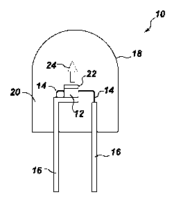
[0020] A lighting apparatus or light emitting assembly or lamp 10 according to
one
embodiment of the present invention is shown in FIG. 1. Lighting apparatus 10
includes a
semiconductor radiation source, shown as light emitting diode (LED) chip 12,
and leads 14
electrically attached to the LED chip. The leads 14 may be thin wires
supported by a thicker
lead frame(s) 16 or the leads may be self supported electrodes and the lead
frame may be
omitted. The leads 14 provide current to LED chip 12 and thus cause it to emit
radiation.
[0021] The lamp may include any semiconductor blue or UV light source that is
capable of
producing white light when its emitted radiation is directed onto the
phosphor. In one
embodiment, the semiconductor light source is a blue emitting LED doped with
various
impurities. Thus, the LED may comprise a semiconductor diode based on any
suitable III-V,
II-VI or IV-IV semiconductor layers and having an emission wavelength of about
250 to 550
nm. In particular, the LED may contain at least one semiconductor layer
comprising GaN,
ZnSe or SiC. For example, the LED may comprise a nitride compound
semiconductor
represented by the formula IniGaiAlkN (where Oj; 01(
and I + j + k =1) having an
emission wavelength greater than about 250 nm and less than about 550 nm. In
particular
embodiments, the chip is a near-uv or blue emitting LED having a peak emission
wavelength
from about 400 to about 500 nm. Such LED semiconductors are known in the art.
The
radiation source is described herein as an LED for convenience. However, as
used herein,
the term is meant to encompass all semiconductor radiation sources including,
e.g.,
semiconductor laser diodes. Further, although the general discussion of the
exemplary
structures of the invention discussed herein is directed toward inorganic LED
based light
sources, it should be understood that the LED chip may be replaced by another
radiation
source unless otherwise noted and that any reference to semiconductor,
semiconductor
LED, or LED chip is merely representative of any appropriate radiation source,
including, but
not limited to, organic light emitting diodes.
[0022] The LED chip 12 may be encapsulated within a shell 18, which encloses
the LED
chip and an encapsulant material 20. The shell 18 may be, for example, glass
or plastic.
Preferably, the LED 12 is substantially centered in the encapsulant 20. The
encapsulant 20
- 5 -
CA 02921044 2016-02-10
WO 2015/027202 PCT/US2014/052376
is preferably an epoxy, plastic, low temperature glass, polymer,
thermoplastic, thermoset
material, resin or other type of LED encapsulating material as is known in the
art. Optionally,
the encapsulant 20 is a spin-on glass or some other high index of refraction
material.
Preferably, the encapsulant material 20 is an epoxy or a polymer material,
such as silicone.
Both the shell 18 and the encapsulant 20 are preferably transparent or
substantially optically
transmissive with respect to the wavelength of light produced by the LED chip
12 and
phosphor blend 22, which contains a Mn+4 doped phosphor according to the
present
invention. Alternately, the lamp may 10 may only comprise an encapsulant
material without
an outer shell 18. The LED chip 12 may be supported, for example, by the lead
frame 16, by
the self supporting electrodes, the bottom of the shell 18, or by a pedestal
(not shown)
mounted to the shell or to the lead frame. In some embodiments, the LED chip
12 is
mounted in a reflective cup (not shown). The cup may be made from or coated
with a
reflective material, such as alumina, titania, or other dielectric powder
known in the art,
particularly alumina.
[0023] Lighting apparatus 10 includes phosphor blend 22, radiationally coupled
to the LED
chip 12. Radiationally coupled means that the elements are associated with
each other so
radiation from one is transmitted to the other. Phosphor blend 22 is deposited
on the LED
12 by any appropriate method. For example, a water based suspension of the
phosphor(s)
can be formed, and applied as a phosphor layer to the LED surface. In one such
method, a
silicone slurry in which the phosphor particles are randomly suspended is
placed around the
LED. This method is merely exemplary of possible positions of phosphor blend
22 and LED
12. Thus, phosphor blend 22 may be coated over or directly on the light
emitting surface of
the LED chip 12 by coating and drying the phosphor suspension over the LED
chip 12. Both
the shell 18 and the encapsulant 20 should be transparent to allow white light
24 to be
transmitted through those elements. Although not intended to be limiting, in
some
embodiments, the median particle size of the phosphor composition ranges from
about 1 to
about 25 microns, particularly from about 15 to about 20 microns.
[0024] In other embodiments, phosphor blend 22 is interspersed within the
encapsulant
material 20, instead of being formed directly on the LED chip 12. The phosphor
(in the form
of a powder) may be interspersed within a single region of the encapsulant
material 20 or,
more preferably, throughout the entire volume of the encapsulant material.
Blue light
emitted by the LED chip 12 mixes with the light emitted by phosphor blend 22,
and the mixed
light appears as white light. If the phosphor is to be interspersed within the
material of
encapsulant 20, then a phosphor powder may be added to a polymer precursor,
loaded
- 6 -
269305
=
around the LED chip 12, and then the polymer precursor may be cured to
solidify the
polymer material. Other known phosphor interspersion methods may also be used,
such
as transfer loading.
[0025] In yet another embodiment, phosphor blend 22 is coated onto a surface
of the shell
18, instead of being formed over the LED chip 12. The phosphor composition is
preferably
coated on the inside surface of the shell 18, although the phosphor may be
coated on the
outside surface of the shell, if desired. Phosphor blend 22 may be coated on
the entire
surface of the shell or only a top portion of the surface of the shell. The
UV/blue light
emitted by the LED chip 12 mixes with the light emitted by phosphor blend 22,
and the
mixed light appears as white light. Of course, the phosphor may be located in
any two or
all three locations or in any other suitable location, such as separately from
the shell or
integrated into the LED.
[0026] FIG. 2 illustrates a second structure of the system according to the
present
invention. Corresponding numbers from FIGS. 1-4 (e.g. 12 in FIG. 1 and 112 in
FIG. 2)
relate to corresponding structures in each of the figures, unless otherwise
stated. The
structure of the embodiment of FIG. 2 is similar to that of FIG. 1, except
that the phosphor
material 122 is interspersed within the encapsulant material 120, instead of
being formed
directly on the LED chip 112. The phosphor (in the form of a powder) may be
interspersed
within a single region of the encapsulant material or, more preferably,
throughout the entire
volume of the encapsulant material. Radiation emitted by the LED chip 112
mixes with the
light emitted by the phosphor 122, and the mixed light appears as white light
124. If the
phosphor is to be interspersed within the encapsulant material 120, then a
phosphor
powder may be added to a polymer precursor, and loaded around the LED chip
112. The
polymer precursor may then be cured to solidify the polymer. Other known
phosphor
interspersion methods may also be used, such as transfer molding.
[0027] FIG. 3 illustrates a third possible structure of the system according
to the present
invention. The structure of the embodiment shown in FIG. 3 is similar to that
of FIG. 1,
except that the phosphor material 222 is coated onto a surface of the envelope
218, instead
of being formed over the LED chip 212. The phosphor material 222 is preferably
coated
on the inside surface of the envelope 218, although the phosphor may be coated
on the
outside surface of the envelope, if desired. The phosphor 222 may be coated on
the entire
surface of the envelope, or only a top portion of the surface of the envelope.
The radiation
226 emitted by the LED chip 212 mixes with the light emitted by the phosphor
222, and the
- 7 -
CA 2921044 2018-04-24
CA 02921044 2016-02-10
WO 2015/027202 PCT/US2014/052376
mixed light appears as white light 224. Of course, the structures of FIGS. 1-3
may be
combined, and the phosphor may be located in any two or all three locations,
or in any other
suitable location, such as separately from the envelope, or integrated into
the LED.
[0028] In any of the above structures, the lamp 10 {as exemplified in FIG.
1) may also
include a plurality of scattering particles (not shown), which are embedded in
the
encapsulant material. The scattering particles may comprise, for example,
alumina or
titania. The scattering particles effectively scatter the directional light
emitted from the LED
chip, preferably with a negligible amount of absorption.
[0029] As shown in a fourth structure in FIG. 4, the LED chip 412 may be
mounted in a
reflective cup 430. The cup 430 may be made from or coated with a reflective
material, such
as alumina, titania, or other dielectric powders known in the art,
particularly alumina. The
remainder of the structure of the embodiment of FIG. 4 is the same as those of
any of the
previous figures, and can include two leads 416, a conducting wire 432, and an
encapsulant
material 420. The reflective cup 430 is supported by the first lead 416 and
the conducting
wire 432 is used to electrically connect the LED chip 412 with the second lead
416.
[0030] Another structure (particularly for backlight applications) is a
surface mounted
device ("SMD") type light emitting diode 550, e.g. as illustrated in FIG. 5.
This SMD is a
"side-emitting type" and has a light-emitting window 552 on a protruding
portion of a light
guiding member 554. The SMD type light emitting diodes 550 can be made by
disposing
LEDs that have been formed beforehand by flow soldering or the like on a glass
epoxy
substrate, whereon an electrically conductive pattern has been formed and
covering the LED
with the window 552. An SMD package may comprise an LED chip as defined above,
and a
phosphor material that is excited by the light emitted from the LED chip.
[0031] When used with an LED emitting at from 350 to 550 nm and one or more
other
appropriate phosphors, the resulting lighting system will produce a light
having a white color,
the characteristics of which will be discussed in more detail below. Lamp 10
may also
include scattering particles (not shown), which are embedded in the
encapsulant material.
The scattering particles may comprise, for example, alumina or titania. The
scattering
particles effectively scatter the directional light emitted from the LED chip,
preferably with a
negligible amount of absorption.
[0032] In addition to the color stable Mn+4 doped phosphor, phosphor blend 22
may include
one or more other phosphors. When used in a lighting apparatus in combination
with a blue
- 8 -
CA 02921044 2016-02-10
WO 2015/027202 PCT/US2014/052376
or near UV LED emitting radiation in the range of about 250 to 550 nm, the
resultant light
emitted by the assembly will be a white light. Other phosphors such as green,
blue, orange,
or other color phosphors may be used in the blend to customize the white color
of the
resulting light and produce higher CRI sources. When used in conjunction with
a LED chip
emitting at from, e.g., 250 to 550 nm, the lighting apparatus preferably
includes a blue
phosphor for converting some, and preferably all, of the LED radiation to blue
light, which in
turn can then be efficiently converted by the color stable Mn+4 phosphors and
phosphor
blends of the present invention. Suitable phosphors for use in phosphor blends
according to
the present invention include, but are not limited to,
(Ba,Sr,Ca)5(PO4)3(CI,F,Br,OH):Eu2+,Mn2+; (Ba,Sr,Ca)BP05:Eu2+,Mn2+;
(Sr,Ca)10(PO4)6*vB203:Eu2+ (wherein 0<v1); Sr2Si308*2SrCl2:Eu2+;
(Ca,Sr,Ba)3MgSi208:Eu2+,Mn2+; BaA18013:Eu2+; 2SrO*0.84P205*0.1 66203:Eu2+;
(Ba,Sr,Ca)MgA110017:Eu2+,Mn2+; (Ba,Sr,Ca)A1204:Eu2+;
(Y,Gd,Lu,Sc,La)B03:Ce3+,Tb3+;
ZnS:Cu+,CI-; ZnS:Cu+,A13+; ZnS:Ag+,CI-; ZnS:Ag+,A13+; (Ba,Sr,Ca)2Si1_04_2:Eu2+
(wherein
00.2); (Ba,Sr,Ca)2(Mg,Zn)Si207:Eu2+; (Sr,Ca,Ba)(AI,Ga,ln)2S4:Eu2+;
(Y,Gd,Tb,La,Sm,Pr,Lu)3(AI,Ga)5,012-3/2,:Ce3+ (wherein 0cc0.5);
(Ca,Sr)8(Mg,Zn)(SiO4)4C12:Eu2+,Mn2+; Na2Gd2B207:Ce3+,Tb3+;
(Sr,Ca,Ba,Mg,Zn)2P207:Eu2+,Mn2+; (Gd,Y,Lu,La)203:Eu3+,Bi3+;
(Gd,Y,Lu,La)202S:Eu3+,Bi3+;
(Gd,Y,Lu,La)VO4:Eu3+,Bi3+; (Ca,Sr)S:Eu24,Ce3+; SrY2S4:Eu2+; CaLa2S4:Ce3+;
(Ba,Sr,Ca)MgP207:Eu2+,Mn2+; (Y,Lu)2W06:Eu3+,Mo6+; (Ba,Sr,Ca)0Si1N,:Eu2+
(wherein
213+47=30; Ca3(Sia4)C12:Eu2+; (Lu,Sc,Y,Tb)2_CevCa1-wl-iMg2_wPw(Si,Ge)3_,N012-
u/2 (where
0<v).1, and 0vir0.2); (Y,Lu,Gd)2_,CacSi4N6,,C1,:Ce3+, (wherein Oc.p0.5);
(Lu,Ca,Li,Mg,Y)alpha-SiAION doped with Eu2+ and/or Ce3+;
(Ca,Sr,Ba)SiO2N2:Eu2+,Ce3+;
3.5MgO*0.5MgF2*Ge02:Mn4+; Cai_c_fCecEufAli+cSii_cN3, (where 0<c50.2, 05.N0.2);
Ca1-h-
rCenEurAli_h(Mg,Z11)hSiN3, (where 0<110.2, 00.2); Ca1-23-
tCe5(Li,Na)3EutAISiN3, (where
s+t>0); and Cal (5, oCe,(Li,Na),EuAli+,õ,Sii,+,N3, (where (:)=:30.2,
0<xg.4, 04D:).2)
[0033] The ratio of each of the individual phosphors in the phosphor blend may
vary
depending on the characteristics of the desired light output. The relative
proportions of the
individual phosphors in the various embodiment phosphor blends may be adjusted
such that
when their emissions are blended and employed in an LED lighting device, there
is produced
visible light of predetermined x and y values on the CIE chromaticity diagram.
As stated, a
white light is preferably produced. This white light may, for instance, may
possess an x
value in the range of about 0.30 to about 0.55, and a y value in the range of
about 0.30 to
- 9 -
CA 02921044 2016-02-10
WO 2015/027202 PCT/US2014/052376
about 0.55. As stated, however, the exact identity and amounts of each
phosphor in the
phosphor composition can be varied according to the needs of the end user.
[0034] When combined with a LED emitting at from 350-550 nm and, optionally,
one or
more additional phosphors, the use of a phosphor according to the present
invention allows
for a white LED device having a higher CRI value and lower CCT as compared to
a cerium
doped terbium aluminum garnet (TAG) based lighting device. LED devices having
OCT
values from about 2500 to about 10000, preferably from 2500 to 4500, and high
CRI values
from about 70 to 95 can be made. This allows for an increased ccx coordinate
and a
reduced ccy coordinate on the CIE color chromaticity diagram for the LED
device, resulting
in a "warmer" color LED.
[0035] The color stable Mn+4 doped phosphors of the present invention may be
used in
applications other than those described above. For example, the material may
be used as a
phosphor in a fluorescent lamp, in a cathode ray tube, in a plasma display
device or in a
liquid crystal display (LCD). The material may also be used as a scintillator
in an
electromagnetic calorimeter, in a gamma ray camera, in a computed tomography
scanner or
in a laser. These uses are merely exemplary and not limiting.
EXAMPLES
General Procedures
Annealing Procedure
[0036] The PFS phosphor was placed in a furnace chamber. The furnace chamber
was
evacuated using a mechanical pump and purged multiple times with nitrogen and
nitrogen,
fluorine mixtures. After several pump and purge cycles, the furnace chamber
was filled with
an atmosphere containing 20% fluorine gas and 80% nitrogen gas to a pressure
of about
1 atmosphere. The chamber was then heated to the desired anneal temperature.
After
holding for about 8 hours, the chamber was cooled to room temperature. The
fluorine
nitrogen mixture was evacuated, the chamber was filled and purged several
times with
nitrogen to ensure the complete removal of fluorine gas before opening the
chamber.
- 10-
CA 02921044 2016-02-10
WO 2015/027202 PCT/US2014/052376
Preparation of Treatment Solutions
[0037] Aqueous solutions containing HF were prepared using 48% HF (w/w) and
solutions
containing H2SiF6 were prepared using 35% H2SiF6 (w/w). Where K2SiF6 was used,
it was
added to the solution which was stirred for 30 minutes after the addition,
then gravity filtered
through a 2.7 micron pore size filter paper to remove undissolved K2SiF6.
Aqueous Solution Treatment
[0038] The phosphor (3 g.) was slowly added to the solution (26 ml), and the
mixture was
stirred for 20 minutes. The phosphor was allowed to settle for 1 minute, then
the
supernatant was decanted and the treated phosphor was filtered, rinsed with
acetone 3
times, dried under vacuum for 3 hours and sifted.
High Temperature High Humidity (HHTH) Stability Testing
[0039] Samples for high temperature, high humidity (HTHH) treatment were made
by mixing
phosphor powders into a two-part methyl silicone binder (RTV-615, Momentive
Performance
Materials) in a ratio of 0.9 g phosphor to 0.825 g silicone (parts A+B). The
phosphor/silicone
mixture was then poured into aluminum sample holders and cured at 90 C for 20
minutes.
Control samples were stored under nitrogen, and samples for exposure to HTHH
conditions
were placed into a 85 C/85% RH controlled atmosphere chamber. These HTHH
samples
were removed after 300 hours and their luminescence intensity under 450 nm
excitation
compared to that of the control samples.
-11 -
269305
High Light Flux Conditions (Laser Damage) Stability Testing
[0040] A laser diode emitting at 446 nm was coupled to an optical fiber with a
collimator
at its other end. The power output was 310 mW and the beam diameter at the
sample was
700 microns. This is equivalent to a flux of 80 W/cm2 on the sample surface.
The spectral
power distribution (SPD) spectrum that is a combination of the scattered
radiation from the
laser and the emission from the excited phosphor is collected with a 1 meter
(diameter)
integrating sphere and the data processed with the spectrometer software
(SpecwinTm).
At intervals of two minutes, the integrated power from the laser and the
phosphor emission
were recorded (by integrating the SPD from 400nm to 500nm and 550 rim to 700
nm
respectively). The first 90 minutes of the measurement are discarded to avoid
effects due
to the thermal stabilization of the laser. The percentage of intensity loss
due to laser
damage is calculated as follows:
(Power ¨ Initial power)
Intensity loss (%) = 100 ______________________ = Laser Damage
Initial power
While only the emitter power from the phosphor is plotted, the integrated
power from the
laser emission as well as its peak position was monitored to ensure that the
laser remained
stable (variations of less than 1%) during the experiment.
COMPARATIVE EXAMPLES 1-4
[0041] Control materials that were not exposed to the aqueous treatment
included the as-
synthesized PFS phosphor, that is, material that was not heat treated
(Comparative
Example 1) and the PFS phosphor after F2 annealing (Comparative Example 3).
The same
materials were also treated with the HF solution containing K2SiF6 as
described in
US 8,252,613 (Comparative Examples 2 and 4).
EXAMPLES 1-7
[0042] In Examples 1-5, the as-synthesized PFS phosphor (without heat
treatment) were
treated with aqueous solutions as shown in Table 1. In Examples 6 and 7, the
PFS
phosphor was annealed under a fluorine atmosphere before treatment with the
hexafluorosilicic acid solutions shown in Table 1.
- 12 -
CA 2921044 2018-04-24
CA 02921044 2016-02-10
WO 2015/027202 PCT/US2014/052376
Table 1
HF, ml H2SiF6, ml K2Si F6, g
Comparative Example No.
1 NA NA NA
2 26 0 1.4
Example No.
1 20 6 1.4
2 13 13 1.4
3 6 20 1.4
4 0 26 1.4
0 26 0
Comparative Example No.
3 NA NA NA
4 26 1.4
Example No.
6 0 26 1.4
7 0 26 0
[0043] The phosphors of Examples 1-7 and Comparative Examples 1-4 were
subjected to
HHTH conditions and evaluated for laser damage. Results are shown in Table 2.
For these
experiments, plaque measurements of the powder had a standard deviation of
0.6% for
absorbance measurements (Abs.), 1.7% for quantum efficiency measurements (QE)
and 2%
for high temperature, high humidity (HTHH) measurements. The standard
deviation for
measuring the quantum efficiency and laser damage of PFS when mixed in a
silicone and
measured in an integrating sphere (tape QE) are less than 0.5%.
- 13-
CA 02921044 2016-02-10
WO 2015/027202 PCT/US2014/052376
Table 2
Ex. Comp. Tape Laser
no. ex. no Absorbance QE HTHH QE damage Treatment
1 72 100 92 100 8 None
2 71 100 99 102 7.2 100% HF
1 71 98 100 X X
2 71 98 98 X X
3 69 99 100 X X
4 70 98 97 101 6.8 No HF
: 5 1-- 70 99 98 X X No K2SiF6
3 67 100 X 100 0.6 None
4 65 100 X 100 0.6 100% HF
6 64 105 X 101 0.3 No HF
7 66 104 X 102 0.3 No K2S1F6
All aqueous treatments were effective in preventing reduction in intensity
after exposure to
HHTH or high light flux condition compared to untreated controls. Comparative
Example 1
illustrates the loss of properties of an untreated phosphor stability testing.
QE and intensity
after stability testing of the samples of Examples 1-5 was equivalent to or
better than that of
Comparative Example 2, which was treated with a solution containing HF and
K2SiF6, and no
hexafluorosilicic acid. Likewise, performance of the samples of Examples 6 and
7 were
equivalent to or better than that of Comparative Example 4. However, samples
that were
treated with solutions containing no HF produced phosphors had the best
balance of
properties after aging. Examples 4, 6 and 7 showed significant reduction in
laser damage,
while maintaining HHTH performance and maintaining or improving QE.
[0044] No significant change in particle size was measured for samples
produced using any
of the treatment processes. Although the particle size did not change, the
sample of
Example 3 had a tap bulk density that was 1.6x that of Comparative Example 2,
indicating
that the H2SiF6 treated material is less agglomerated than the HF treated
material. The
- 14 -
slight decrease in absorbance measured for the treated samples indicates that
the
manganese content of these samples decreased after treatment.
Example 8: X-ray photoelectron spectroscopy
[0045] Table 3 shows the results of XPS measurements, which provide
elemental analysis
of the surface of the powder and has a detection limit of about 0.1 atomic %.
In agreement
with the plaque absorbance measurements, XPS provides further evidence that
the surface
[Mn] decreases upon treatment to the detection limits of the measurement
system. In
addition, surface carbon and oxygen are also reduced upon treatment.
Table 3
%c %0 %F %K %Si %Mn
Comp. Ex. 1
12.8 1.4 52.1 20.8 12.6 0.21
Ex. No. 4 1.8 0.6 61.5 23.0 13.0 0.06
Ex. No. 3 2.0 0.6 62.1 22.4 12.7 0.07
Comp. Ex. 2 6.0 1.0 58.3 21.6 13.1 0.03
[0046] While only certain features of the invention have been illustrated and
described
herein, many modifications and changes will occur to those skilled in the art.
It is,
therefore, to be understood that the appended claims are intended to cover all
such
modifications and changes as fall within the scope of the invention.
- 15 -
CA 2921044 2017-10-18