Note: Descriptions are shown in the official language in which they were submitted.
CA 02921513 2016-02-22
ELECTRONIC DEVICE INCLUDING PATCH ANTENNA ASSEMBLY HAVING
CAPACITIVE FEED POINTS AND SPACED APART CONDUCTIVE SHIELDING
VIAS AND RELATED METHODS
Field of the Invention
[0001] The present invention relates to the field of
electronic devices, and, more particularly, to patch antennas
and related methods.
Background
[0002] A patch antenna, for example, a microstrip patch
antenna may provide a relatively a high gain for a given area
using a relatively simple printed circuit construction, thus
making its use widespread. One type of microstrip patch
antenna has a radiation pattern that extends broadside to the
patch plane. Such a microstrip antenna is commonly fed using
a probe, for example, in the form of a connector pin or a
circuit board via to form the probe that carries current to
the patch surfaces.
[0003] However, the radiation bandwidth of a microstrip
patch antenna may be limited. For example, the half power (3
dB) instantaneous gain bandwidth of microstrip patch antennas
may be less than 20 percent in practice. This may be
particularly disadvantageous compared to other types of
antennas, such as parabolic reflector antennas, which can
operate over many octaves of bandwidth. The frequency
response of a simple, square, half wave edge, linearly
polarized microstrip patch antenna may be described based upon
the quadratic equation (ax2+ bx +c = 0) so there may be a
"single hump" gain maxima located about a first, half wave
resonance.
[0004] The bandwidth of a microstrip patch antenna
increases linearly based upon the thickness of the substrate
1
CA 02921513 2016-02-22
, .
on which it is carried, so doubling the substrate thickness
may double the bandwidth and halving the substrate thickness
may halve the bandwidth. Unfortunately however, problems may
arise in a broadband application using a relatively thick
substrate microstrip antenna, as the feed probe can radiate in
a manner akin to a monopole antenna. Given that the radiation
pattern of a feed probe is different than that of the patch
itself, the combined thick substrate patch radiation produces
an asymmetric pattern and reduced realized gain.
[0005] U.S. Patent No. 6,181,279 to Van Hoozen discloses a
patch antenna with an electrically small ground plate using
peripheral parasitic stubs. More particularly, Van Hoozen
discloses the parasitic stubs or shielding element is for
segregating electromagnetic fields between the patch antenna
and the ground plate.
[0006] U.S. Patent No. 5,515,057 to Lennen et al. is
directed to a GPS receiver with an n-point symmetrical feed
double-frequency patch antenna. More particularly, Lennen et
al. discloses n symmetrical feed points that are placed
geometrically on the patch antenna to achieve circular
polarization of the GPS receiver with an n-point antenna.
[0007] Further improvements to patch antennas may be
desired. For example, it may be particularly desirable to
increase bandwidth, gain, directivity, and radiation pattern
symmetry.
Summary
[0008] An electronic device may include wireless
communications circuitry, and an antenna assembly coupled to
the wireless communications circuitry. The antenna assembly
may include a substrate, an electrically conductive layer
defining a ground plane carried by the substrate, and an
electrically conductive patch antenna element carried by the
substrate and spaced from the ground plane. The electrically
2
CA 02921513 2016-02-22
, .
conductive patch antenna element may have a symmetric axis
dividing the electrically conductive patch antenna element
into first and second symmetric areas. The electrically
conductive patch antenna element may have first and second
feed openings in the first and second symmetric areas,
respectively, and first and second feed pads in the first and
second feed openings, respectively, defining first and second
capacitive feed points. The antenna assembly may also include
first and second feed lines extending through the substrate
and respectively coupling the first and second feed pads to
the wireless communications circuitry, and a plurality of
spaced apart conductive shielding vias coupled to the ground
plane and extending through the substrate surrounding the
electrically conductive patch antenna element. Accordingly,
the electronic device may provide increased efficiency, for
example, by providing increased bandwidth, gain, and
directivity.
[0009] The electrically conductive patch antenna element
may have at least one bucking opening therein. The substrate
may include at least one bucking recess aligned with the at
least one bucking opening, for example. The antenna assembly
may further include at least one conductive bucking via
coupled to the ground plane and extending to the at least one
bucking recess, for example.
[0010] The electronic device may further include phase
delay circuitry carried by the substrate and coupled to at
least one of the first and second feed lines. The phase delay
circuitry may include at least one meander line, for example.
[0011] The antenna assembly may further include at least
one resonator coupled to each of the first and second
capacitive feed points. The at least one resonator may
include at least one conductive X-shaped resonator, for
example.
3
CA 02921513 2016-02-22
. .
[0012] The electronic device may further include a
dielectric cover layer carried by the electrically conductive
patch antenna element. The dielectric cover layer may have a
relative permittivity and a relative permittivity within 20%
of each other. The substrate may have a relative permittivity
and a relative permittivity within 20% of each other, for
example.
[0013] A method aspect is directed to a method of making an
antenna assembly. The method may include forming an
,
electrically conductive patch antenna element on a substrate
and spaced from an electrically conductive layer defining a
ground plane. The electrically conductive patch antenna
element may be formed to have a symmetric axis dividing the
electrically conductive patch antenna element into first and
second symmetric areas. The electrically conductive patch
antenna element may be formed to have first and second feed
openings in the first and second symmetric areas,
respectively. The method may further include forming first
and second feed pads in the first and second feed openings,
respectively, defining first and second capacitive feed
points. The method may also include forming first and second
feed lines extending through the substrate and respectively
coupling the first and second feed pads to wireless
communications circuitry, and forming a plurality of spaced
apart conductive shielding vias coupled to the ground plane
and extending through the substrate surrounding the
electrically conductive patch antenna element.
[0014] Another embodiment is directed to an electronic
device that includes wireless communications circuitry and an
antenna assembly coupled to the wireless communications
circuitry. The antenna assembly may include a substrate, an
electrically conductive layer defining a ground plane carried
by the substrate, and an electrically conductive patch antenna
element carried by the substrate and spaced from the ground
4
CA 02921513 2016-02-22
. .
plane. The electrically conductive patch antenna may have a
symmetric axis dividing the electrically conductive patch
antenna element into first and second symmetric areas. The
electrically conductive patch may have first and second feed
openings in the first and second symmetric areas,
respectively, and first and second feed pads in the first and
second feed openings, respectively, defining first and second
capacitive feed points. The antenna assembly may also include
first and second feed lines extending through the substrate,
one of the first and second feed lines coupling a respective
one of the first and second feed pads to the wireless
communications circuitry and another of the first and second
feed lines being electrically floating, and a plurality of
spaced apart conductive shielding vias coupled to the ground
plane and extending through the substrate surrounding the
electrically conductive patch antenna element.
[0015] The ground plane may have at least one opening
therein. The substrate may include at least one recess
aligned with the at least one opening, for example. The
another one of the first and second feed lines may extend to
the at least one recess.
[0016] The antenna assembly may further include at least
one resonator coupled to each of the first and second
capacitive feed points. The at least one resonator may be an
X-shaped resonator.
[0017] The electronic device may further include a
dielectric cover layer carried by the electrically conductive
patch antenna element. The dielectric cover layer may have a
relative permittivity and a relative permittivity within 20%
of each other. The substrate may have a relative permittivity
and a relative permittivity within 20% of each other, for
example.
[0018] A corresponding method of making an antenna assembly
may include forming an electrically conductive patch antenna
CA 02921513 2016-02-22
. .
element on a substrate and spaced from an electrically
conductive layer defining a ground plane ground plane. The
electrically conductive patch antenna may be formed to have a
symmetric axis dividing the electrically conductive patch
antenna element into first and second symmetric areas. The
electrically conductive patch antenna element may also be
formed to have first and second feed openings in the first and
second symmetric areas, respectively. The method may also
include forming first and second feed pads in the first and
second feed openings, respectively, defining first and second
capacitive feed points and forming first and second feed lines
extending through the substrate, one of the first and second
feed lines coupling a respective one of the first and second
feed pads to wireless communications circuitry and another of
the first and second feed lines being electrically floating.
The method may further include forming a plurality of spaced
apart conductive shielding vias coupled to the ground plane
and extending through the substrate surrounding the
electrically conductive patch antenna element.
Brief Description of the Drawings
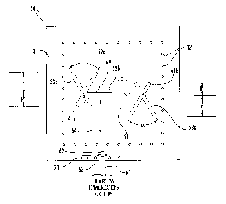
[0019] FIG. 1 is top schematic view of an electronic device
according to an embodiment of the present invention.
[0020] FIG. 2 is a bottom schematic view the electronic
device of FIG. 1.
[0021] FIG. 3 is a schematic cross-sectional view of an
antenna assembly in accordance with an embodiment of the
present invention.
[0022] FIGS. 4A and 4B are simulated radiation pattern cuts
of the antenna assembly of FIG. 1.
[0023] FIG. 5 is a schematic cross-sectional view of the
antenna assembly of an electronic device according to another
embodiment.
6
CA 02921513 2016-02-22
. .
[0024] FIG. 6 is a top schematic view of the antenna
assembly of FIG. 5.
[0025] FIG. 7 is a bottom schematic view of the antenna
assembly of FIG. 5.
[0026] FIGS. 8A and 8B are simulated radiation pattern cuts
of the antenna assembly of FIG. 5.
[0027] FIG. 9 is a graph of the simulated realized gain
response of the antenna assembly of FIG. 5.
[0028] FIG. 10 is a Smith Chart of the simulated impedance
of the antenna assembly of FIG. 5.
[0029] FIG. 11 is a graph of the simulated VSWR response
the antenna assembly of FIG. 5.
[0030] FIG. 12 is a top schematic view of an array of
antenna assemblies according to another embodiment.
[0031] FIG. 13 is a bottom schematic view of the array of
antenna assemblies of FIG. 12.
Detailed Description
[0032] The present invention will now be described more
fully hereinafter with reference to the accompanying drawings,
in which preferred embodiments of the invention are shown.
This invention may, however, be embodied in many different
forms and should not be construed as limited to the
embodiments set forth herein. Rather, these embodiments are
provided so that this disclosure will be thorough and
complete, and will fully convey the scope of the invention to
those skilled in the art. Like numbers refer to like elements
throughout, and prime and multiple prime notations are used to
indicate similar elements in alternative embodiments.
[0033] Referring initially to FIGS. 1-3, an electronic
device 20 includes wireless communications circuitry 21 and an
antenna assembly 30 coupled to the wireless communications
circuitry. The wireless communications circuitry 21 may
include a wireless transceiver, just a transmitter, just a
7
CA 02921513 2016-02-22
. .
receiver, and/or an RF power source, for example. The
wireless communications circuitry 21 may include other and/or
additional circuitry for wireless communication. As will be
appreciated by those skilled in the art, the antenna assembly
30 may be considered a reciprocal device useful for both
transmitting and receiving.
[0034] The antenna assembly 30 may be in the form of a
microstrip patch antenna for linear polarization, and
illustratively includes a substrate 31 and an electrically
conductive layer defining a ground plane 32 carried by the
substrate. The ground plane 32 is illustratively carried
within the substrate 31, for example, sandwiched between two
dielectric layers of the substrate. In some embodiments, the
ground plane 32 may be carried by a lower surface of the
substrate 31 or by another portion of the substrate. The
antenna assembly 30 may be realized as a multilayer circuit
board. Additional ground plane layers may be included.
[0035] The antenna assembly 30 also includes an
electrically conductive patch antenna element 33 carried by an
upper surface of the substrate 31. The electrically
conductive patch antenna element 33 is illustratively spaced
from the ground plane 32.
[0036] The electrically conductive patch antenna element 33
illustratively is in the shape of a rectangle, and more
particularly, a square. Of course the electrically conductive
patch antenna element 33 may have another shape, for example,
a circular shape.
[0037] The electrically conductive patch antenna element 33
has a symmetric axis 34 that divides the electrically
conductive patch antenna element into first and second
symmetric areas 35a, 35b. The electrically conductive patch
antenna element 33 has first and second feed openings 36a, 36b
in the first and second symmetric areas 35a, 35b,
respectively. While a particular symmetric axis 34 is
8
CA 02921513 2016-02-22
, .
illustrated, it should be understood that the symmetric axis
may be aligned differently than as illustrated, for example,
it may be diagonally oriented.
[0038] The electrically conductive patch antenna element 33
also includes first and second feed pads in the first and
second feed openings 36a, 36b, respectively, defining first
and second capacitive feed points 37a, 37b. The electrically
conductive patch antenna element 33 also includes first and
second feed lines 41a, 41b extending through the substrate 31
and respectively coupling the first and second feed pads or
first and second capacitive feed points 37a, 37b to the
wireless communications circuitry 21. The first and second
feed lines 41a, 41b may be in the form of a plated through-
hole via, a metal connector pin, rivet, hookup wire, or other
feed structure as will be appreciated by those skilled in the
art.
[0039] The first and second capacitive feed points 37a, 37b
capacitively couple currents to the electrically conductive
patch antenna element 33 across the air gap therebetween. The
first and second capacitive feed points 37a, 37b may cancel
distributed inductance of the first and second feed lines 41a,
41b.
[0040] Distributed inductance of the first and second feed
lines 41a, 41b and the distributed capacitance of the first
and second capacitive feed points 37a, 37b together form a
series resonant circuit which may provide a double tuned
antenna system for increased bandwidth. The double tuning may
form a 4th order Chebyschev response with, selected for
passband ripple, a maximally flat Butterworth response, or
other response shapes as will be appreciated by those skilled
in the art.
[0041] The first and second capacitive feed points 37a, 37b
are illustratively oriented as a diamond shape relative to the
electrically conductive patch antenna element 33. This may
9
CA 02921513 2016-02-22
, .
reduce reflections to the passage of currents on the surface
of the electrically conductive patch antenna element 33. Of
course the first and second capacitive feed points 37a, 37b
may be oriented as a square, i.e., aligned with, the
electrically conductive patch antenna element 33, or have
other shapes as well.
[0042] Radiation from the second feed line 41b is toward
the opposite side of the electrically conductive patch antenna
element 33 than radiation from the first feed line 41a.
Radiation from the first and second feed lines 41a, 41b may
therefore counteract each other to produce a more symmetric
radiation pattern with a beam maximum more normal to the
electrically conductive patch antenna element 33. It may be
desirable to drive the first and second feed lines 41a, 41b at
equal power and drive the second feed line at a delayed phase
relative the first feed line. The delayed phase applied to
the second feed line 42b is denoted by p and approximately
given by:
p = - (360 f s) / [ (c "q (srpr) ] degrees
Where:
p = the phase delay applied to the second feed line 41b
relative to the first feed line 41a;
360 = a constant equal to the number of degrees in a cycle;
f = the operating frequency in Hertz;
c = the speed of light in meters / second;
s = the spacing between the vias in meters;
cr = the substrate relative permittivity (dimensionless); and
pr = the substrate relative permeability if any
(dimensionless).
[0043] The minus sign occurs as a convention for adding
phase shift (increased time delay). The equation derives from
microstrip transmission line theory as this is the phase delay
between the first and second feed lines 41a, 41b for a current
traveling across the electrically conductive patch antenna
CA 02921513 2016-02-22
. .
element 33. In one prototype the first feed line 41a was at 0
degrees phase and the second feed line 41b was at -168 degrees
phase.
[0044] Prior art circular polarized patches use multiple
fed probes and quadrature phasing (superimposing cosine and
sine current distributions) to cause a traveling wave current
distribution on the patch. Additionally, prior art circular
polarized patches implement quadrature phasing according to
the Pythagorean identity:
cpõ --- cos 2 e + sin2 (e + 9o0 - 9Q0) = cos2 0 + sin2 O.
Differently, the embodiments described herein may use multiple
feed lines with non-quadrature phasing (i.e., not 0, 90, 180
or 270 phase) and still render circularly polarized radiation
on the patch.
[0045] Differently, the disclosed embodiments implement the
feed line phasing according to:
(NI = - (360 f s) / [ (c "Ni (Er r) ] degrees.
[0046] Spaced apart conductive shielding vias 42 are
illustratively conductively connected to the ground plane 32
and extend through the substrate 31 surrounding the
electrically conductive patch antenna element 33. The spaced
apart conductive shielding vias 42 may provide an
electrostatic shield to further attenuate unwanted radiation
from the first and second feed lines 41a, 41b. The spaced
apart conductive shielding vias 42 generally do not make
electrical contract at their tops which may reduce capacitance
between the conductive shielding vias and edges of the
electrically conductive patch antenna element 33, and reduces
their becoming loops or otherwise shielding radiation from the
electrically conductive patch antenna element 33. The
electromagnetic waves formed by the first and second feed
lines 41a, 41b generally cannot pass through the comb like
11
CA 02921513 2016-02-22
. .
electrostatic shield provided by the conductive shielding vias
42. The electromagnetic wave(s) formed by edges of the
electrically conductive patch antenna element 33 generally do
not have to pass through the conductive shielding vias 42 so
the desired radiation occurs freely.
[0047] The electrically conductive patch antenna element 33
illustratively has first and second bucking openings 44a, 44b
therein. The substrate 31 has respective bucking recesses
45a, 45b aligned with the bucking openings 44a, 44b.
[0048] Respective conductive bucking vias 46a, 46b are
coupled to the ground plane 32, and each extends to the level
of the corresponding bucking recess 45a, 45b. The bucking
vias 46a, 46b reduce undesirable radiation from the first and
second feed lines 41a, 41b. Each bucking via 46a, 46b and
feed line 41a, 41b carry a current flow in opposite directions
to reduce via radiated fields, e.g. anti-parallel current
flows. The bucking vias 46a, 46b and first and second feed
lines 41a, 41b may together form an open wire transmission
line, as will be appreciated by those skilled in the art.
[0049] Each bucking recess 45a, 45b may have a conical
shape and may be formed by drilling downwardly from above and
into the substrate 31, for example. This may advantageously
reduce capacitance between each bucking via 46a, 46b and the
electrically conductive patch antenna element 33. The conical
point of the drill bit, for example: 1) forms a hole in the
electrically conductive patch antenna element 33 and 2)
reduces the height of each bucking via 46a, 46b so that the
bucking via does not reach the plane of the electrically
conductive patch antenna element 33.
[0050] Reduced capacitance between the bucking vias 46a,
46b and the electrically conductive patch antenna element 33
may increase bucking via current. As vias may typically be
formed as plated through holes, and plating only part of the
hole is difficult and undesirable, the countersink drilling
12
CA 02921513 2016-02-22
. .
may advantageously allow a via of partial height to be formed,
as will be appreciated by those skilled in the art.
[0051] The electronic device 20 may further include phase
delay circuitry 51 carried by the substrate 31 and coupled to
the first and second feed lines 41a, 41b. The phase delay
circuitry 51 illustratively includes a respective meander line
52a, 52b carried along a bottom surface of the substrate 31
for each of the first and second feed lines 41a, 41b.
[0052] The antenna assembly 30 further includes a
respective resonator 53a, 53b coupled to each of the first and
second feed capacitive points 37a, 37b. Each resonator 53a,
53b is conductive and illustratively an X-shape and the
asymmetric X-shape as illustrated in FIG. 2. It is understood
that an X-shape may include both symmetric X-shapes and
assymetric X-shapes. Of course, there may be any number of
resonators and arms. Additionally, each resonator 53a, 53b
may have a different shape. X-shaped conductive resonators
53a, 53b may force a higher order polynomial response by
increasing the number of passband ripples, as will be
appreciated by those skilled in the art. The impedance
response of the X-shaped conductive resonators 53a, 53b, and,
in turn, the antenna frequency response, may be adjusted by
the changing the overall length a+b of each the X-shaped
conductive resonators and the spread angle a between the arms.
Spread angle a adjusts the Q factor of the X-shaped resonators
53a, 53b. The length a+b adjusts the resonant frequency of
each resonator 53a, 53b; in other words a bigger X-shaped
conductive resonator has self resonance at lower frequency and
a physically smaller one resonates at a higher frequency. A
preferred length for a+b may be that length which results a
half wave resonance from X-shaped resonator arm tip to arm
tip. The ratio of a divided by b, e.g. a/b, adjusts the
degree to which each asymmetric X-shaped conductive resonator
electrically couples with to the antenna assembly 30. A
13
CA 02921513 2016-02-22
, .
larger ratio of a/b provides a more asymmetric X-shaped
conductive resonator 53a, 53bm which may couple less into the
antenna assembly 30 electrically, reducing antenna assembly 30
passband ripple. A smaller ratio of a/b means more a
symmetric X-shaped conductive resonator 53a, 53b which may
couple more into the antenna assembly 30 to increase
bandwidth. The X-shaped resonators 53a, 53b allow a tradeoff
between antenna assembly 30 passband ripple amplitude and
overall bandwidth of the antenna assembly 30. Higher ripple
amplitude means more bandwidth. Each resonator 53a, 53b is in
effect one or more resonant circuits in parallel with the
antenna. Each X-shaped conductive resonator 53a, 53b may
typically carry a sinusoidal current distribution. Connecting
the X-shaped conductive resonators 53a, 53b in parallel at the
first and second feed lines 41a, 41b increases the antenna
system 30 polynomial tuning order. A bandwidth increase of 2
to 4 fold, or even more, may be obtained when the X-shaped
resonators 53a, 53b are included in the antenna assembly 30,
depending on the trades of selected ripple level, spread angle
a, and X-shaped conductive resonators 53a, 53b arm length.
[0053] The first and second feed lines 41a, 41b may be fed
by a coaxial antenna feed line 61 from the wireless
communications circuitry 21. An outer conductor 63 of the
coaxial antenna feed line 61 is coupled to the ground plane
32, for example, soldered to a via filled ground pad 71 while
an inner conductor 62 of the coaxial antenna feed line is
coupled to a common transmission line 64. The common
transmission line 64 continues to the parallel junction 69
with the first and second feed lines 41a, 41b. RF power
divides at the parallel junction 69 to feed the first and
second feed lines 41a, 41b. The power division may be equal
in most embodiments, but may be unequal if needed to further
synthesize patterns shape, overcome transmission line losses
etc. Positioning transformers the first and second feed lines
14
CA 02921513 2016-02-22
41a, 41b can adjust the branched-off impedances at the
parallel junction 69 and, in turn, that power division ratio.
The antenna assembly 30 may be used independently from the
illustrated onboard wireless communications circuitry 21.
[0054] The antenna assembly 30 may optionally include a
cover layer 48 over the upper surface of the substrate and
covering the first and second feed capacitive points 37a, 37b
and conductive bucking vias 46a, 46b (FIG. 3). The cover
layer 48 may be a substantially nonconductive material and
have a relative permittivity Er within +20%, and more
preferably, equal to, the relative permeability Ar. In other
words Er pr in the cover layer 48. Advantageously, the
characteristic impedance of the cover layer 48 is then nearly
that of free space for all values of Er pr.
This is because
the intrinsic wave impedance in the cover layer 48 is given by
Zcover = 377NI(Er/Ar) Ohms, and the term Er/pr generally always
equals 1 whenever Er and Ar are the same in value so the result
is or about 377 Ohms. 377 Ohms is, of course, the wave
impedance of free space. The further advantage of an Er pr
cover layer 48 with Zcover 377
ohms is that the cover layer is
then reflection-less for all values of the thicknesses of the
cover layer. This is because cover layer 48 reflection
coefficient is given by 11 = (Zfreespace Zcover) (Zcover
Zfreespace) and since the intrinsic wave impedance of the cover
layer is 377 ohms or nearly so, the numerator term of the
equation is small or zero. The Er -,-, Ar cover layer 48 has an
intrinsic wave velocity according to v = C/\/(ErAr), so the wave
may be appreciably miniaturized, and antenna size is
proportional to the wavelength size, so the Er fir
cover layer
48 may have substantial miniaturizing effect on antenna
assembly 30. A smaller antenna assembly 30 may be possible
for a given frequency. In some embodiments, the substrate 31
may likewise have properties of a relative permittivity and a
relative permittivity within +20% of each other, and more
CA 02921513 2016-02-22
. .
particularly, Er --,- pr, and which may provide a similarly
miniaturized substrate with time delay, group delay, and
differential phase that is more constant over frequency.
Example cr -', pr cover layer materials 48 may include light
nickel zinc ferrites such as mix 68 by Fair Rite of Wallkill,
New York, or material M5 by National Magnetics Group - TCI
Ceramics of Bethlehem, Pennsylvania. Of course mixes of
magnetic and dielectric powders may be used with binders to
achieve a cover layer 48 with a desired value of cr P= /Ir.
[0055] Referring to FIGS. 4A and 4D, a comparison of the
radiation patterns of the antenna assembly 30 with and without
one of the feed lines 41a, 41b will now be described. These
radiation patterns are the E field plane cuts in polar
coordinates. As background, E plane and H plane designation
is a shorthand to describe the orientation of linearly
polarized antennas, and for the antenna assembly 30' both the
first and second feed lines 41a, 41b physically lie in that E
field plane. So this is the radiation pattern cut in the plane
of the probes.
[0056] Traces 504, 506 are the realized gain data in units
of dBi. Realized gain includes material losses and mismatch
losses. As can be seen, adding a second feed line 41a, 41b
increased the radiation pattern symmetry and caused the
broadside (elevation angle 9 - 0) gain of a specific example
embodiment to increase from 5.6 dBi to 8.5 dBi for a realized
gain increase of 1.9 dBi. Advantageously, the radiation
pattern was righted so peak pattern amplitude occurred nearly
exactly at patch plane perpendicular when the additional feed
line 41a, 41b was included. An additional feed line, e.g.,
one of the feed lines 41a, 41b, may be added to a patch
antenna at little to no cost increase at the same time as the
first feed line is manufactured.
[0057] A method aspect is directed to a method of making
the antenna assembly 30. The method includes forming an
16
CA 02921513 2016-02-22
electrically conductive patch antenna element 33 on a
substrate 31 and spaced from an electrically conductive layer
defining a ground plane 32. The electrically conductive patch
antenna element 33 is formed to have a symmetric axis 34
dividing the electrically conductive patch antenna element
into first and second symmetric areas 35a, 35b. The
electrically conductive patch antenna element 33 is formed to
have first and second feed openings 36a, 36b in the first and
second symmetric areas 35a, 35b, respectively.
[0058] The method includes forming first and second feed
pads in the first and second feed openings, respectively,
defining first and second capacitive feed points 37a, 37b.
The method also includes forming first and second feed lines
41a, 41b extending through the substrate 31 and respectively
coupling the first and second feed pads 37a, 37b to wireless
communications circuitry 21. The method also includes forming
a plurality of spaced apart conductive shielding vias 42
coupled to the ground plane 32 and extending through the
substrate 31 surrounding the electrically conductive patch
antenna element 33.
[0059] Referring now to FIGS. 5-7, in another embodiment
the antenna assembly 30' includes a substrate 31' and an
electrically conductive layer defining a ground plane 32'
carried by the substrate. The antenna assembly 30' also
includes an electrically conductive patch antenna element 33'
carried by the substrate 31' and spaced from the ground plane
32'. The antenna assembly 30' may not include a multilayer
type printed circuit board, and therefore may be more economic
to manufacture than the antenna assembly 30 embodiment
described above.
[0060] The electrically conductive patch antenna element
33' has a symmetric axis 34' dividing the electrically
conductive patch antenna element into first and second
symmetric areas 35e, 35b'. The electrically conductive patch
17
CA 02921513 2016-02-22
. .
antenna element 33' has first and second feed openings 36a',
36b' in the first and second symmetric areas 35a', 35b',
respectively. First and second feed pads are in the first and
second feed openings, respectively, defining first and second
capacitive feed points 37a', 37b'.
[0061] The antenna assembly 30' also includes first and
second feed lines 41a', 41b' extending through the substrate
31'. In the illustrated embodiment, one of the first and
second feed lines 41a' couples a respective one of the first
and second feed pads 36a' to the wireless communications
circuitry 21' (i.e., a drive feed line) and the other of the
first and second feed lines 41b' is electrically floating.
[0062] The ground plane 32' has an opening 56' therein.
The substrate 31' also has a recess 57' therein aligned with
the opening 56' in the ground plane 32'. The recess 57' may
be conically shaped, for example. The electrically floating
feed line 41b' illustratively extends downwardly from the
electrically conductive patch antenna element 33' to the
recess 57'.
[0063] As will be appreciate by those skilled in the art,
the electrically floating feed line 41b' may be considered a
parasitic feed line and may provide useful radiation pattern
symmetry without a microstrip power divider or an additional
printed circuit board layer to drive it. The electrically
floating feed line 41b' makes electrical contact with first
and second capacitive feed points 37a', 37b' at an upper end
thereof and makes no electrical contact with the ground plane
32' at a lower end thereof. An open circuit exists at the
lower end of the electrically floating or parasitic feed line
41b' due to the conically shaped recess 57' and opening 56' in
the ground plane 32'. The capacitive feed point 37b' adjacent
the electrically floating feed line 41b' may have the same
dimensions as the other capacitive feed point 37a'. In some
18
CA 02921513 2016-02-22
. .
embodiments, the first and second capacitive feed points 37a',
37b' may have different sizes.
[0064] The electrically floating feed line 41b' receives
electric current from the electrically conductive patch
antenna element 33'. The electric current on the electrically
floating feed line 41b' causes monopole-like radiation, which
counteracts radiation by the drive feed line 41a'. Radiation
from the drive feed line 41a' squints the radiation pattern
off broadside in the direction of the drive feed line, while
radiation from the electrically floating feed line 41b'
squints the radiation pattern in the direction of the
electrically floating feed line. Combined radiation from the
first and second feed lines 41a', 41b' (i.e., drive and
electrically floating feed lines) steers the antenna radiation
pattern to broadside or nearly so.
[0065] Referring to the graphs in FIGS. 7A and 7B,
radiation patterns of the antenna assembly 30' with and
without an electrically floating feed line 41b' will now be
described. The patterns in FIGS. 7A and 7B are E field plane
cuts. E plane and H plane is a shorthand to describe linearly
polarized antenna physical orientations and for the antenna
assembly 30'. Both the first and second feed lines 41a', 41b'
physically lie in that E field plane. Traces 604, 606 are the
simulated realized gain data in units of dBi. Realized gain
includes material losses and mismatch losses. As can be seen,
inclusion of the electrically floating feed line 41b'
increased the radiation pattern symmetry and caused the
broadside (p = 0) gain to increase from 5.6 dBi to 8.5 dBi, a
change of 1.9 dBi. The pattern peak with the electrically
floating feed line 41b' was only 8 from patch plane broadside
and only 0.3 dB lower in realized gain at patch plane normal.
Advantageously, the electrically floating feed line 41b'
pattern improvements occurred without having to configure a
power divider other apparatus to drive the electrically
19
CA 02921513 2016-02-22
. .
floating feed line. Further, since at least one probe, the
first feed line 41', is being implemented, adding the
electrically floating feed line 41b' to a design can be
negligible in cost. Table 1 further describes the
characteristics of the example embodiment antenna assembly 30'
from which the radiation patterns were obtained:
Table 1: Antenna Assembly 30' Example Parameters
Antenna type Square microstrip patch, IA 2\
edges nominal, probe driven.
Special feature Electrically floating feed
line 41b', driven by patch
through a capacitor pad
Application Earth station antenna for AO-
50 and A0-78 satellites
Construction method Suspended microstrip (very
thin PWB provides patch
element atop a thick foam
substrate)
Analysis method Finite element simulation
using Ansys HFSS, plus
validation with a physical
prototype.
Center frequency 436.795 MHz (may be scaled for
other frequencies)
Polarization Linear
Electrically conductive patch 9.345 x 9.345 inches
antenna element 33' size
Substrate 31' Material Styrene Foam
CA 02921513 2016-02-22
Substrate 31' thickness 2.172 inches, 0.082\air
Substrate 31' relative 1.045 (relative permittivity
permittivity Er is a dimensionless number)
Ground plane 32' size 28.8 x 28.8 inches
First and second feed lines #22 copper wire, passed
41a', 41b' material through drilled hole and
soldered to patch.
First feed line 41a location 2.339 inches from radiating
(driving probe location edge
Electrically floating feed Image point, 2.339 inches from
line 41b' location opposite radiating edge
X-shaped conductive resonators Not used in this example.
53a, 53b
Top cover 49 Not used in this example.
First and second capacitive 0.654 x 0.654 inches
feed points 37a', 37b'
(capacitor pad size)
Matching capacitor gap, around 0.050 inches
first and second capacitive
feed points 37a', 37b'
Matching capacitor electrical About 3.74 picofarads. This
value, first and second capacitor bucks the feed probe
capacitive feed points 37a', inductance and double tunes
37b' the antenna.
Radiation pattern shape Single broadside lobe,
21
CA 02921513 2016-02-22
. ,
approximately cos' fan shape
Realized gain, at patch plane +8.5 dBi, linear polarization
broadside
Realized gain, at look angle +8.8 dBi, at A = 90 p = 8
of peak radiation pattern linear polarization
amplitude
3 dB gain beamwidth 56
3 dB gain bandwidth 158 MHz or 35.4 %
Passband characteristic Double tuned: two gain peaks
with a 1 dB ripple there
between.
[0066] FIG. 8 is a graph of the swept gain analyzed for the
Table 1 antenna assembly 30'. Trace 704 is the realized gain
response over frequency. Two peaks 706, 708 can be seen as
well as a dip 710. The difference between the peaks 706, 708
and the dip 701 define a response ripple that is small, less
than 1 decibel.
[0067] The Smith Chart of FIG. 9 is the driven (not
floating) feed line 41a' impedance at the ground plane
penetration. Trace 804 is a sweep of the impedance data
points in frequency. The Smith Chart of FIG. 12 presents the
reflection coefficient Sil. Crossover 806 represents the two
gain peaks 706, 708 from the graph of FIG. 8. Moving the
driven (not floating) feed line 41a' towards the patch edge
moves the trace locus 804 to the right, and moving the driven
(not floating) feed line 41a' towards the patch center moves
the trace locus 804 to the left in the Smith Chart of FIG. 9.
Marker data 808 shows the vector impedance at specific
frequencies after being normalized to 50 Ohms.
22
CA 02921513 2016-02-22
. .
[0068] The graph of FIG. 10 shows a simulated voltage
standing wave ratio (VSWR) trace 902 as measured at the driven
(not floating) feed line 41a' in a 50 Ohm system. The
simulation was based upon a 2.17 inch thickness polystyrene
foam sheet for the antenna substrate 31'. The bandwidth could
be further extended with a thicker substrate material, for
example. The Table 1 example and data thereof should not be
construed as limiting the scope of possible antenna
embodiments.
[0069] Including one or more electrically floating feed
lines is beneficial for most varieties of patch antennas,
including patch elements of many shapes, including circular or
polygonal shapes, and for stacked patch antennas. A plurality
of electrically floating feed lines can be used to improve
radiation from dual polarization patch antennas, such as
antennas providing simultaneous dual linear polarization and
or simultaneous dual circular polarization.
[0070] Similarly to the embodiment described above with
respect to FIGS. 1-3, spaced apart conductive shielding vias
42' are coupled to the ground plane 32' and extend through the
substrate 31' surrounding the electrically conductive patch
antenna element 33'.
[0071] A coaxial connector 65' is carried by the bottom of
the substrate 31'. The ground plane 22' has an opening 66'
therein to allow passage of the first feed line 41e, or drive
feed line, to pass therethrough for coupling with an inner
conductor of a coaxial cable, for example. The body 67' of
the coaxial connector 65', which illustratively includes
threads 68' for coupling to a mating coaxial cable connector
for example, is coupled to the ground plane 32' and also
couples the outer conductor of the coaxial cable to the ground
plane. The antenna assembly 30 may be used independently from
the illustrated onboard wireless communications circuitry 21.
23
CA 02921513 2016-02-22
. .
[0072] A method aspect is directed to a method of making
the antenna assembly 30'. The method includes forming an
electrically conductive patch antenna element 33' on a
substrate 31' and spaced from an electrically conductive layer
defining a ground plane 32'. The electrically conductive
patch antenna element 33' is formed to have a symmetric axis
34' dividing the electrically conductive patch antenna element
into first and second symmetric areas 35a', 35b'. The
electrically conductive patch antenna element 33' is also
formed to have first and second feed openings 36a', 36h' in
the first and second symmetric areas 35a', 35b', respectively.
[0073] The method includes forming first and second feed
pads in the first and second feed openings 36a', 36bf,
respectively, defining first and second capacitive feed points
37a', 37bf. The method also includes forming first and second
feed lines 41a', 41b' extending through the substrate 31'.
One of the first and second feed lines 41a' couples a
respective one of the first and second capacitive feed points
37a' to wireless communications circuitry 21' and another of
the first and second feed lines 41b' is electrically floating.
The method also includes forming spaced apart conductive
shielding vias 42' coupled to the ground plane 32' and
extending through the substrate 31' surrounding the
electrically conductive patch antenna element 33'.
[0074] Referring now to FIGS. 12 and 13, an array 30"
embodiment is now described. Illustratively, a common
substrate 31" carries four electrically conductive patch
antenna elements 33", 133", 233", 333", each being
symmetrical and with corresponding first and second capacitive
feed points and first and second feed lines as described above
with respect to FIGS. 3-5 (i.e., each having a drive feed line
41a", 141a", 241a", 341a" and an electrically floating
feed line 41b", 141b", 241b", 341b"). The array
24
CA 02921513 2016-02-22
. .
advantageously increases the radiation pattern symmetry by
mitigating undesired feed probe radiation.
[0075] Moreover, the array 30" causes symmetric, broadside
radiation. The electrically conductive patch antenna elements
33", 133", 233", 333" are alternately "clocked" so half of
the electrically conductive patch antenna elements are rotated
180 degrees mechanically with respect to the others. The
clocking enhances radiation pattern symmetry because if
individual element radiation patterns are squinted off
broadside/plane normal, the alternate clocked elements will
radiate in the other direction cancelling the squint. The
mechanically clocked elements are fed with an additional 180
degrees of electrical phase delay using an added length from
the microstrip branch from the radial power divider, or in
other words, from different length meander lines 52", 152" f
252", 352".
[0076] The embodiments described herein may, for example,
advantageously mitigate unwanted radiation from microstrip
patch antenna feed probes, increase patch antenna radiation
bandwidth, reduce patch antenna size, and improve patch
antenna radiation pattern symmetry. Additionally, it should
be appreciated that the antenna assembly may be a circular
polarization patch antenna assembly, as well as a dual channel
linear polarization antenna assembly, and a dual channel
circular polarization assembly.
[0077] Many modifications and other embodiments of the
invention will come to the mind of one skilled in the art
having the benefit of the teachings presented in the foregoing
descriptions and the associated drawings. Therefore, it is
understood that the invention is not to be limited to the
specific embodiments disclosed, and that modifications and
embodiments are intended to be included within the scope of
the appended claims.