Note: Descriptions are shown in the official language in which they were submitted.
I
AMPLIFYING STAGE WORKING POINT DETERMINATION
Field of the invention
The present invention relates to an amplifier circuit. The present invention
also relates
to a method for an amplifier circuit. The present invention also relates to a
computer
program and to a computer program product.
Related art and background of the invention
There is a very large, and still rapidly growing, demand for wireless
communication
services today. Mobile telephone services are used to a very large extent,
e.g. for
telephone conversations and text messages. Also, high speed wireless
communication
is used for a large number of applications, such as internet browsing,
streaming of
music, films and/or television, and the like.
Since the demand for wireless communication services is very high, and the end
users
expect the wireless services to be available essentially everywhere they go,
the wireless
communication system coverage must cover very large geographical areas, both
indoors and outdoors, and also provide high bitrates in these areas.
Traditionally, radio
base stations, such as Base Transceiver Stations (BTS) and eNodeBs, typically
being
located close to a tower comprising one or more tower-mounted antennas, are
provided
with all the circuitry necessary for sending and receiving the wireless
communication
signals to and from the mobile equipments connecting to it, such as Mobile
Stations
(MS) or User Equipments (UEs). The radio base stations have typically been
arranged
in cells. The radio base stations include both the circuitry to receive and
transmit signals
from and to a core network and to receive and transmit signals from and to the
one or
more antennas, including radio frequency (RF) circuits and power amplifiers.
The
mobile equipment also include the
CA 2921898 2019-08-27
CA 02921898 2016-02-19
WO 2015/030663 PCT/SE2014/050985
2
circuitry for receiving and transmitting signals from and to the radio base
stations,
including radio frequency (RF) circuits and power amplifiers.
Also, the end users nowadays expect high speed wireless communication
services,
such as mobile telecommunication services, wireless fidelity networks (WiFi),
and
Wireless Local Area Networks (WLANs), to be available essentially everywhere.
Therefore, a large number of different types of radio transmitting units are
distributed
in indoor and outdoor locations, such as in malls, railway tunnels, road
tunnels,
restaurants, cafés, airports, conference centers, tunnels, stadiums and
exhibition
halls.
Distributed systems have been developed for providing coverage and high
bitrates in
locations for which the traditional radio base station concept results in poor
service
coverage and bitrates. One example of such a distributed system is a
Distributed
Antenna System (DAS). In a DAS one or more Remote Units (RUs), each possibly
being utilized by one operator/service provider and providing one system
and/or
service, are connected to one or more Remote Unit Controllers (RUCs) and/or
one or
more fiber cables. Typically, the one or more RUCs are radio base stations,
such as
a BTS or an eNodeB or the like. These radio base stations provide RF signals
related
to one or more services and/or service providers to the RUs via fiber cables.
The
RUs transmit/receive the RF signals to/from the mobile equipment.
Also, smaller cells have been developed, such as pico cells and femto cells,
which
can be used for increasing coverage and bitrates, and to lower the costs. The
micro
base stations and pico base stations are complete standalone radio base
stations,
including all the circuitry of the traditional radio base stations, including
all the
circuitry necessary for sending and receiving the wireless communication
signals to
and from the mobile equipment, including power amplifiers. The pico cells and
femto
cells can be deployed such that coverage and bitrates can be optimized for the
geographical area of the communication system, both outdoors and indoors.
A further development of the smaller cell concept is the Remote Radio Head
(RRH)
concept. The RRH concept breaks up the traditional radio base station
architecture
into a possibly centrally located processing facility, a so called RRH
controller, and
CA 02921898 2016-02-19
WO 2015/030663 PCT/SE2014/050985
3
one or more distributed antennas units, in this document called RRH units,
being
connected to the processing facility through a network preferably having a
high
bandwidth. Here, all the traditional radio base station processing equipment
except
for the radio frequency processing equipment and the power amplification
equipment
are located in the RRH controller, whereas the radio frequency processing
equipment
and power amplification equipment are located in the distributed RRH units.
As has been described above, there are today a number of concepts available
for
providing and extending the coverage of mobile services and for enhancing the
bitrates at certain locations in the systems. There are also a number of other
such
concepts available for extending the coverage and/or enhancing the bitrates.
In all of
these concepts, a radio signal is transmitted between a radio base
station/RU/RRH
and a mobile equipment of some kind over an air interface. This transmission
over
the air interface requires for all of these concepts for an amplification of
the signals to
be transmitted. This amplification is typically performed by utilization of
one or more
power amplifiers.
Power amplifiers are often utilized as the last amplifier in a transmission
chain, i.e. at
the output of the transmission chain. The power amplifiers are thus
responsible for
providing an RF output signal having a sufficient signal power to an antenna
arrangement. Generally, the signal power should be high enough to provide a
predetermined transmission coverage and/or error rate for the radio
transmission.
However, the signal power, and also other features of the transmitted signals,
must
be kept within predetermined limits, in order to reduce interference in the
radio
transmission system into which the radio signal is transmitted.
There are a number of different classes of amplifiers that are used for power
amplification, such as classes A, B, AB, C, D, E, and additional classes, e.g.
Doherty
amplifiers.
Class A amplifiers utilize the whole input signal for the amplification and
the
conductive element in the amplifier conducts during the whole amplification
cycle
time. Class A amplifiers are simple and add relatively little distortion to
the signal.
CA 02921898 2016-02-19
WO 2015/030663 PCT/SE2014/050985
4
Class B amplifiers only utilize half of the input signal for the amplification
and the
conductive element in the amplifier conducts during half of the amplification
cycle
time. Class B amplifiers are power efficient but add a relatively large amount
of
distortion and/or non-linearity to the signal.
Class AB power amplifiers can be seen as a compromise between class A and
class
B amplifiers. The class AB amplifier generally operates the same way as the
class B
amplifier over half the amplification cycle time, but also conducts a small
part on the
other half of the cycle. Class AB amplifiers thereby sacrifice some power
efficiency
over class B amplifiers, but gains in linearity. Class AB amplifiers are
typically much
more power efficient than class A amplifiers.
Class C amplifiers conduct less than half of the input signal and the
distortion at the
output is high. However, high power efficiencies are possible. A common
application
for class C amplifiers is in RF transmitting devices operating at a single
fixed carrier
frequency, where the distortion is controlled by a tuned load of the
amplifier. The
input signal is used to switch the active device, which causes pulses of
current to flow
through a tuned circuit being a part of the load. The tuned circuit resonates
at one
frequency, e.g. at the fixed carrier frequency, which suppresses the unwanted
frequencies, and the wanted full signal can be extracted by the tuned load.
A Doherty amplifier is a hybrid configuration including a primary/carrier
stage in
parallel with an auxiliary/peak stage. The input signal is split in order to
drive the two
amplifying stages, i.e. the primary/carrier stage and the auxiliary/peak
stage. A
combining network sums the output signals from the two amplifying stages and
phase shifting networks are used at the inputs and outputs of the Doherty
amplifier.
During periods of low signal level, the primary/carrier stage efficiently
operates on the
signal and the auxiliary/peak stage is cutoff, whereby the amplifier consumes
little
power. During periods of high signal level, the primary/carrier stage delivers
its
maximum power and the auxiliary/peak stage delivers up to its maximum power.
The
primary/carrier stage can be implemented e.g. by use of a class B amplifier or
by a
class C amplifier. The auxiliary/peak stage can be implemented e.g. by use of
a class
C amplifier.
CA 02921898 2016-02-19
WO 2015/030663 PCT/SE2014/050985
Usage of power amplification in communication systems for amplification of the
RF
signals, which is necessary in order to provide sufficient coverage and
bitrates, has a
problem in lack of linearity of the power amplifiers. Non-linearity of the
power
amplifiers prevents the power amplifiers to accurately reproduce the signal
being
5 applied to its input port. Also, non-linear power amplifiers used in a
transmitter in a
communication system cause the transmitted signal to leak into adjacent
frequency
radio frequencies/channels, which creates distortion in these adjacent radio
frequencies/channels.
The non-linearity of the power amplifiers limits the performance of the whole
communication system. Non-linearities in the frequency response of the power
amplifiers create distortions that also limit the dynamic range of the
amplifiers. Also,
the created distortions degrade the overall system performance since the
distortions
are transmitted over the air interface of the communication system, whereby
other
signals and/or entities in the communication system can be distorted.
A large number of solutions, e.g. utilizing predistortion, have previously
been
presented in order to solve these problems. When predistortion is utilized, an
inverse
model of the assumed amplifier distortion is introduced into the amplifier
input. The
idea is that the predistortion should cancel out the distortion such that the
predistortion and the distortion together result in an amplifier circuit
having linear gain
and phase. However, such previously known solutions tend to decrease the
amplifier
efficiency while maintaining a high current consumption. Also, the previously
known
solutions increase the hardware complexity and cost considerably.
Aim and most important features of the invention
It is an object of the present invention to provide an amplifier circuit and
an
amplification method that solves the above stated problem.
Hence, according to a first aspect of the present invention, an amplifier
circuit is
provided, comprising an amplifying stage and a predistortion stage and being
arranged for outputting an output signal Xo. The predistortion stage is
arranged for
providing a predistortion signal Xp to be added to an input signal Xin of the
amplifier
circuit in order to compensate for non-linearites of said amplifying stage.
Further, the
CA 02921898 2016-02-19
WO 2015/030663 PCT/SE2014/050985
6
amplifier circuit comprises a working point unit arranged for determining a
suitable
working point WP suitable suitable to be used for the amplifying stage based
on the predistortion
signal ;, and for adjusting an actual working point P W
¨ = actual being used by the
amplifying stage towards the suitable working point VVP
¨ suitable-
According to a second aspect of the present invention, a method for an
amplifier
circuit is provided, wherein the amplifier circuit includes an amplifying
stage and a
predistortion stage and outputs an output signal Xo. The predistortion stage
provides
a predistortion signal ; to be added to an input signal Xin of the amplifier
circuit in
order to compensate for non-linearites of the amplifying stage. The method
comprises determining a suitable working point WP suitable suitable to be used
for the
amplifying stage based on the predistortion signal ;, and adjusting an actual
working point WP
8c181 actual being used by the amplifying stage towards the suitable
working point WP
suitable.
suitable=
According to a third aspect, there is provided a computer program which when
run in
a computer causes the computer to execute the method according to the second
aspect of the present invention.
According to the present invention a suitable working point WIP ¨. suitable to
be used by an
amplifying stage is determined based on a predistortion signal ; being
provided by a
predistortion stage. An actual working point VVP
actual being used by the amplifying
stage is then adjusted towards the suitable working point WPsuitable, which is
determined based on the predistortion signal X.
Hereby, an optimal working condition for the amplifying stage can be
automatically
found and maintained. This optimal working condition can by the present
invention be
reached when the amplification efficiency is at its maximum, at the same time
as the
gain and linearity of the amplifier circuit is preserved.
A reduction of the power consumption and a more linear power amplification can
hereby be achieved. The reduced power consumption that can be achieved by the
present invention also results in extended component lifetimes due to lowered
working temperatures for the amplifier circuit according to the present
invention.
CA 02921898 2016-02-19
WO 2015/030663 PCT/SE2014/050985
7
Since the suitable working point P W
- = suitable determination is based on the predistortion
signal ;, a dynamic working point WP
¨= suitable determination is achieved. Thus an
adjustment to current transmission and/or signal situation/scenarios is
possible by
usage of the present invention.
The present invention can be implemented mainly in the software and therefore
adds
very little to the hardware complexity and/or production costs.
In this document, the present invention is presented mainly for its
implementation on
class AB amplifiers and on Doherty amplifiers. However, as is clear for a
skilled
person, the present invention can of course be utilized together with
essentially any
power amplifier being used for amplifying RF signals.
The adjustment of the actual working point WP ¨. actual of the amplifying
stage may for
example include adjustment of a gate-source voltage, VGS, for the amplifying
stage.
The amplifying stage may for example comprise one or more transistors (e.g.
field-
effect transistors) and the adjustment of the actual working point WPactuai of
the
amplifying stage may for example include adjustment of one or more gate-source
voltages for the one or more transistors. The adjustment of the actual working
point
WPactual of the amplifying stage may for example include adjustment of one or
more
gate-source voltages for the one or more transistors of the amplifying stage,
while
maintaining one or more drain-source voltages, VDS, for the one or more
transistors
constant. The amplifying stage may for example include a Doherty configuration
amplifier or a class AB amplifier including one or more amplifier chains for
which one
or more gate-source voltages are adjusted as part of adjusting the actual
working
point WPactual of the amplifying stage.
Brief description of the drawings
Fig. 1 shows an amplifier circuit according to an embodiment of the present
invention.
Fig. 2 shows an amplifier circuit according to an embodiment of the present
invention.
Fig. 3 shows an amplifier circuit according to an embodiment of the present
invention.
Fig. 4 shows an amplifier circuit according to an embodiment of the present
invention.
CA 02921898 2016-02-19
WO 2015/030663 PCT/SE2014/050985
8
Fig. 5 shows a flow chart diagram of a method according to an embodiment of
the
present invention.
Fig. 6 schematically shows a radio communication system.
Detailed description of preferred embodiments
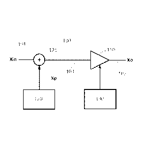
Figure 1 schematically shows an amplifier circuit 100 according to the present
invention. The amplifier circuit 100 amplifies an input signal Xin being
applied on an
input 101 of the amplifier circuit 100. The amplifier circuit 100 includes an
amplifying
stage 110 and a predistortion stage 120. The predistortion stage 120 is
arranged for
providing a predistortion signal ;, which is added to the input signal Xin in
a
combiner 121. By adding the predistortion signal ; to the input signal Xin, a
compensation for non-linearities later being added by the amplifying stage 110
is
provided. Thus, the signal being outputted at the combiner output 103 is a
combined
input and predistortion signal Xin+Xp. The combined input and predistortion
signal
Xin+Xp is then amplified in the amplifying stage 110. The amplifier circuit
100 further
includes an output 102, on which the amplified predistorted output signal X0
is
outputted;
According to the present invention, the working point unit 130 is arranged for
determining a suitable working point VVP ¨. suitable to be used by the
amplifying stage
110. The working point unit 130 is arranged to base the determination of this
suitable
working point WP suitable suitable on the predistortion signal ; being
provided by the
predistortion stage 120. The working point unit 130 is further arranged for
adjusting
an actual working point VV.. Pactuai being used by the amplifying stage 110
towards the
suitable working point \AP
¨= suitable determined based on the predistortion signal X.
Hereby, an optimal working condition for the amplifying stage 110 can be
automatically found and maintained. By driving the amplifying stage 110 at an
optimal working condition, a reduced power consumption and a more linear power
amplification is achieved.
Also, since the suitable working point WP
suitable suitable determination is based on the
predistortion signal Xp, a dynamic working point WP
¨= suitable determination is achieved,
CA 02921898 2016-02-19
WO 2015/030663 PCT/SE2014/050985
9
which adjusts to the current transmission and/or signal situation/scenario.
Thus, a
dynamic and automatic adjustment of the working point WP
¨= suitable, e.g. based on a
number of carriers currently used, a currently used power level, or a current
number
of users within a carrier, can be achieved by the amplifier circuit according
to the
present invention.
Also, an extended component lifetime can be achieved by use of the amplifier
circuit
according to the present invention. This is due to the fact that the lower
power
consumption of the amplifier circuit 100 of the present invention results in a
lower
working temperature for the present amplifier circuit 100. Lower working
temperatures reduce the risk for component failure in electrical circuitry in
general,
and for amplifier circuits in particular.
Implementation of the present invention in a transmission unit, for example in
a Multi
Carrier Power Amplifier (MCPA) being designed to amplify at least two radio
signals
at different carrier frequencies, can be done with very little addition to the
hardware
and/or production costs, since the hardware needed for implementation of the
present invention is already present in predistortion amplifiers of today.
Thus, the
present invention can be implemented in the software, without additional
hardware.
Therefore, the additional cost for implementing the present invention is very
small.
Figure 2 schematically shows an amplifying stage 110 of an amplifier circuit
100
according to an embodiment of the present invention. Here, the amplifying
stage 110
includes a first 111 amplifier chain and a second 112 amplifier chain, the
first 111 and
second 112 amplifier chains being arranged parallel to each other. The
combined
input and predistortion signal Xin+Xp on the amplifying stage input 103 is
provided to
a splitter 113, which splits the combined input and predistortion signal
Xin+Xp to the
first 111 and second 112 amplifier chains.
The amplifying stage 110 shown in figure 2 illustrates a general class AB
amplifier.
Class AB amplifiers can be arranged in a number of different configurations,
such as
a single amplifier chain configuration, a configuration having two or more
parallel
amplifier chains, a push-pull configuration, or a configuration combining one
or more
CA 02921898 2016-02-19
WO 2015/030663 PCT/SE2014/050985
of these configurations. The one or more amplifier chains in these
configurations are
all arranged for handling essentially the same signal power levels.
For class AB amplifiers, the suitable working point P W
- = suitable, which is determined and
adjusted towards according to the present invention, is the amplifier bias
voltages
5 defining a sweet point for the amplifier chains of the class AB
amplifier. This is
described more in detail below.
An amplifier circuit according to the invention including an amplifying stage
110 as
shown in figure 2 has corresponding advantages as the amplifier circuit shown
in
figure 1 above. Thus, an optimal working condition for the amplifying stage
110 can
10 be automatically and efficiently determined, and can also be maintained
for changing
transmission and/or signal conditions. Hereby, a reduced power consumption, a
more
linear power amplification, and an extended component lifetime are achieved at
a
very moderate additional cost by the amplifier circuit according to the
invention.
Figure 3 schematically shows an amplifying stage of an amplifier circuit 100
according to an embodiment of the present invention. The amplifying stage 110
is
here a Doherty configurated amplifying stage 110. Thus, the amplifier circuit
100
according to this embodiment of the present invention includes a Doherty
configuration amplifying stage 110.
The Doherty amplifying stage 110 includes a first 111 amplifier chain and a
second
112 amplifier chain, the first 111 and second 112 amplifier chains being
arranged
parallel to each other. The combined input and predistortion signal )(in-0(p
on the
amplifying stage input 103 is provided to a splitter and 90 phase shifter
113. The
splitter/phase shifter 113 splits the combined input and predistortion signal
Xin+Xp
and provides the split parts to the first 111 and second 112 amplifier chains,
respectively. The phase of the second part of the combined input and
predistortion
signal Xin+Xp, being provided to the second 112 amplifier chain, is
shifted/delayed
with 90 by the splitter 113.
The first amplifier chain 111 of the amplifying stage 110 is arranged for
amplification
of higher and lower power signals, and the second amplifier chain 112 is
arranged for
amplification only of higher power signals. The first signal S1 of the
combined input
CA 02921898 2016-02-19
WO 2015/030663 PCT/SE2014/050985
11
and predistortion signal Xin+Xp being amplified by the first amplifier chain
111 is
shifted/delayed with 900 by a transmission line 115 having a length
corresponding to
a 90 phase shift, before it is combined with the second signal S2, being an
amplified
second part of the combined input and predistortion signal Xin+Xp, by the
combiner
114. The impedance of the combined first S1 and second S2 signals of the
signal,
i.e. the predistorted and amplified Xin+Xp signal, is then transformed by an
impedance
transformer 116, which for example can perform an impedance transformation
from
25 0, which can be the impedance after the combined 114, to 50 0, which should
be
the impedance for the output signal X0 at the output 102.
An amplifier circuit according to the invention including an Doherty
configuration
amplifying stage 110 as shown in figure 3 has the above mentioned advantages,
i.e.
to be able to provide an efficient determination of an optimal working
condition for the
amplifying stage 110, which can be adjusted during changing transmission
and/or
signal conditions, whereby a reduced power consumption, a more linear power
amplification, and an extended component lifetime are achieved.
Figure 4 shows an amplifier circuit 200 according to an embodiment of the
present
invention. The amplifier circuit includes an input 201 receiving an input
signal )(in, a
predistortion stage 220, a working point stage 230, an amplifying stage 210,
and an
output 202 providing an output signal Xo.
The input signal Xin first reaches a first coupler 221, which couples the
input signal )(in
to a predistorter 224. The input Xin is then delayed by a delay unit 223.
Thereafter a
predistorter signal ; being provided by the predistorter 224 is added to the
input
signal Xin by the second coupler 222. The predistorter 224 determines the
predistorter signal ; based on a comparison of the input signal Xin and the
output
signal X . For example, the predistorter signal ; can be determined such that
the
output signal X looks like the input signal Xin, but amplified. The
predistortion stage
220 outputs a predistorted input signal, i.e. a signal being a combined input
and
predistortion signal Xin+Xp.
The combined input and predistortion signal Xn+Xp is then input to the working
point
stage 230 and is fed to first attenuation unit 231. The first attenuation unit
231
CA 02921898 2016-02-19
WO 2015/030663 PCT/SE2014/050985
12
attenuates the combined input and predistortion signal Xin+Xp based on a
possible
total gain adjustment Va for the amplifier circuit 100.
The attenuated combined input and predistortion signal Xin+Xp is then split up
in a
splitter and 90 phase shifter 213 splitting the attenuated combined input and
predistortion signal Xin+Xp and provides the parts to the first 211 and second
212
amplifier chains, respectively. The phase of the second part of the attenuated
combined input and predistortion signal Xin-EXp being provided to the second
212
amplifier chain is shifted/delayed with 90 by the splitter 213.
In the second amplifier chain 212, the second part of the signal is attenuated
in a
second attenuator 232 based on an initial peaking amplifier gain Vg. The
initial
peaking amplifier gain Vg is here initially set such that the gain of the
first 211 and
second 212 amplifier chains, respectively, are essentially equal when the
output
signal X0 has a maximum power.
From the second attenuator 232, the signal is fed to a phase shifter 233, in
which the
phase of the signal is shifted based on an initial phase setting of the
peaking
amplifier V. The initial phase setting of the peaking amplifier Vp is here
initially set
such that the first signal Si being amplified by the first amplifier chain 211
and the
second signal S2 being amplified by the second amplifier chain 212 are in
phase at
the output 202 when the output signal X has a maximum power. Thus, by usage
of
the phase shifter 233, a phase difference A
¨phase between the first 211 and the second
212 amplifier chains is achieved. Also, by usage of the second attenuator 232,
an
amplitude difference A
¨amplitude between the first 211 and the second 212 amplifier
chains is achieved.
Also, bias voltages for the first amplifier chain 211 Bõ and for the second
212
amplifier chain Bpk are determined by the working point stage 230, and are
thereafter
used for biasing the first 211 and second 212 amplifier chains. The first
amplifier
chain bias voltage Bca is initially set for nominal class AB amplifier bias.
The second
amplifier chain bias voltage Bpk is initially set such that the second
amplifier chain 112
is cut off for lower power signals and is active for higher power signals.
CA 02921898 2016-02-19
WO 2015/030663 PCT/SE2014/050985
13
A current consumption unit 218 is connected to the first 211 and second 212
amplifier chains. The current consumption unit 218 is arranged for
determining, e.g.
by measuring, the amount of current being used by the amplifiers.
The working point stage/unit 230, which can be implemented in a control unit,
is
arranged for determining a suitable working point WP
¨= suitable and for controlling the
second attenuator 232, the phase shifter 233 and the bias voltages Bca, Bpk
for the
first 211 and second 212 amplifier chains. The working point stage/unit 230 is
arranged for performing this determination of the suitable working point WP
suitable
based on one or more of a measured level of the predistortion signal ;, a
measured
level of the output signal X0, and the current consumption.
The amplifier circuit 200 further includes an amplifying stage 210, here being
illustrated as a Doherty configured amplifying stage 110.
The Doherty amplifying stage 210 includes the first 211 amplifier chain and
the
second 212 amplifier chain being arranged in parallel to each other. The first
amplifier
chain 211 is arranged for amplification of higher and lower power signals, and
the
second amplifier chain 212 is arranged for amplification only of higher power
signals.
The first signal Si being amplified by the first amplifier chain 211 is
shifted/delayed
with 90 by a transmission line 215 and is combined with the second signal S2
being
amplified by the second amplifier chain 212. The combined first S1 and second
S2
signals are transformed by an impedance transformer 216, such that the
impedance
of the output signal X0 at the output 202 is 50 n.
As can be seen in the amplifier circuit 200 shown in figure 6, the
predistortion
performed by the predistortion stage 220 is a closed loop predistortion
producing the
predistortion signal ;, which can be seen as a measure of the linearity of the
amplifying stage 210. Thus, the predistortion signal ; can be seen as an error
signal
corresponding to the amplifier non-linearity.
The output signal can be written as:
X0=FpA(Xin+Xp)=Min-FE,
CA 02921898 2016-02-19
WO 2015/030663 PCT/SE2014/050985
14
where X, is the input signal;
X is the output signal;
; is the predistortion signal;
EPA is a transfer function for the amplifying stage;
k is the amplification that can be provided by the amplifying stage; and
E is a residual non-linearity being present on the output signal.
Thus, in a perfect predistortion, the output signal would be Xo=k*Xin, but
since perfect
predistortion is almost impossible to perform, there is almost always a
residual non-
linearity E left in the output signal that cannot be compensated for by the
predistorter.
The predistortion signal ; is preferably chosen such that the residual non-
linearity
is minimized.
By the use of the predistortion signal ;, possibly together with use of a
measure of
the current consumption provided by the current consumption unit 218, when
finding
a suitable working point P W
- = suitable in accordance with the present invention, a very
efficient and exact determination of the suitable working point P W
- = suitable can be
performed.
The above mentioned adjustment of the actual working point WPactual, which is
provided by the present invention, can include an adjustment of one or more
parameters for the amplifying stage 110, 210 including the first 111, 211 and
second
112, 212 parallel amplifier chains.
One such parameter can be a phase difference A
¨phase between the first 111, 211 and
second 112, 212 amplifier chains. When this parameter is adjusted, the phase
shifts
being provided to one or more of the first 111, 211 and second 112, 212
amplifier
chains are adjusted, such that the phase difference A
¨phase between the first 111, 211
and second 112, 212 amplifier chains is altered.
One such parameter can be an amplitude difference A
¨amplitude between the first 111,
211 and second 112, 212 amplifier chains. When this parameter is adjusted, an
attenuation and/or a signal amplification being provided by one or more of the
first
111, 211 and second 112, 212 amplifier chains are adjusted, such that the
amplitude
CA 02921898 2016-02-19
WO 2015/030663 PCT/SE2014/050985
difference A
¨amplitude between the first 111, 211 and second 112, 212 amplifier chains
is altered.
Such parameters can also be a bias voltage for the first 111, 211 amplifier
chain
and/or for the second 112, 212 amplifier chain. Thus, the bias voltages being
used
5 for biasing the amplifiers in the first and/or second amplifier chain,
respectively.
The working point unit 130, 230 is, according to an embodiment of the present
invention, arranged for determining the suitable working point P W
- = suitable, i.e. one of
more of a phase difference A
¨phase between the first 111, 211 and second 112, 212
amplifier chains, an amplitude difference A
¨amplitude between the first 111, 211 and
10 second 112, 212 amplifier chains, and bias voltages being used for
biasing the
amplifiers in the first and second amplifier chain, while keeping a total gain
k for the
amplifier circuit 100, 200 essentially constant. The total gain k being
provided by the
amplifier circuit 100, 200 is here set and maintained by a closed loop
coupling such
that gain variations being generated by changes of one or more of the peaking
15 amplifier gain Vg, the peaking amplifier Vp, or the bias voltages Bga
and Bpk for the
first 211 and second 212 amplifier chains are compensated for by changes of
the
total gain adjustment Va. This compensation by usage of the total gain
adjustment Va
is set to a converging time being considerably longer than a converging time
for the
predistortion signal X. Thus, the total gain k of the amplifier circuit 100,
200 is
maintained essentially constant, while the working point WP
suitable suitable parameters are
chosen in order to optimize the amplifier circuit 100, 200 regarding e.g.
power
consumption and/or linearity. Often a compromise between power
consumption/efficiency and linearity has to be made when optimizing the
working
point WPsuitable parameters.
According to an embodiment of the present invention, the working point unit
130, 230
is arranged for determining the suitable working point P W
¨ = suitable such that an optimal
efficiency and/or linearity is achieved for the output signal Xo.
The amplifying stage 110, 210 can, as is described above, include a number of
different classes of amplifiers. When the amplifying stage 110, 210 includes a
class
AB amplifier, the suitable working point P W
- = suitable being determined and adjusted by
CA 02921898 2016-02-19
WO 2015/030663 PCT/SE2014/050985
16
the present invention is an amplifier bias voltage defining a sweet point for
the class
AB amplifier.
According to an embodiment of the present invention, the working point unit
130, 230
is arranged for determining the suitable working point WP
¨= suitable by use of an iterative
algorithm. There are a number of such iterative algorithms that could be used
for this
suitable working point WP
¨= suitable determination. For example, the iterative algorithm
used can be a gradient descent algorithm, a steepest gradient descent
algorithm, a
conjugate gradient descent algorithm, a Newton-Raphson algorithm, or a secant
variable metric algorithm. Also, essentially any other suitable iterative
equation
solution finding algorithm could be utilized for this determination.
According to an embodiment of the present invention, parameter values
corresponding to a number of suitable working points P W
- = suitable have been calculated
and stored in a Look Up Table (LUT). Thus, the working point unit 130, 230 is
then
arranged for determining the suitable working point P W
- = suitable by use of this Look Up
Table.
According to an embodiment of the present invention, the working point unit
130, 230
is arranged for determining the suitable working point WP
¨= suitable by a combination of
use of an iterative algorithm and use of a Look Up Table. For example, a
coarse
determination can first be made by use of the Look Up Table and then a finer
determination can be made starting from the parameter values from the Look Up
Table and then adjusted by use of the iterative algorithm.
According to an embodiment of the present invention, the working point unit
130, 230
is arranged for dynamically determining suitable working point P W
- = suitable based on
aging of at least one component of the amplifier circuit 100, 200 and/or on a
current
working condition for the amplifier circuit 100, 200.
The current working condition can here include an amplifier circuit
temperature, a
frequency of the input signal Xhi, a number of carriers to be amplified, a
power
consumption for the amplifying stage, or an average output power for the
amplifier
circuit. As is understood by a skilled person, also other parameters can be
included in
the working condition parameters.
CA 02921898 2016-02-19
WO 2015/030663 PCT/SE2014/050985
17
According to an aspect of the present invention, a method for the above
described
amplifier circuit is presented. Figure 5 shows a flow chart diagram for the
method.
The amplifier circuit includes the amplifying stage 110, 210 and the
predistortion
stage 120, 220, and outputs an output signal Xo. The predistortion stage 120,
220
provides a predistortion signal ; to be added to the input signal Xin of the
amplifier
circuit in order to compensate for non-linearites of the amplifying stage 110,
210.
In a first step 501 of the method according to the present invention, a
determination
of a suitable working point MP ¨. suitable to be used for the amplifying stage
110, 210 is
performed based on the predistortion signal X.
In a second step 502 of the method, the actual working point WP
¨= actual being used by
amplifying stage is adjusted towards the determined suitable working point WP
¨= suitable.
As described above, the adjustment of the actual working point P W
¨ = actual includes an
adjustment of one or more of a phase difference A
¨phase between the first 111, 211 and
second 112, 212 amplifier chains, an amplitude difference A
¨amplitude between the first
111,211 and second 112, 212 amplifier chains, a bias voltage for the first
111,211
amplifier chain, and a bias voltage for the second 112, 212 amplifier chain.
The working point unit 130, 230 can according to an embodiment determine the
suitable working point VVP
suitable while keeping a total gain k for the amplifier circuit
essentially constant.
According to an embodiment of the invention, the working point unit 130, 230
determines the suitable working point WPsuitable such that the first signal S1
and the
second signal S2 are in phase when being combined to the output signal Xo.
The working point unit 130, 230, can utilize iterative algorithms and/or Look
Up
Tables when determining the suitable working point WP
= suitable. Such iterative
algorithms may include e.g. a gradient descent algorithm, a steepest gradient
descent algorithm, a conjugate gradient descent algorithm, a Newton-Raphson
algorithm, and a secant variable metric algorithm.
According to an embodiment of the invention, the working point unit (130)
dynamically determines the suitable working point VVP
¨= suitable based on aging of at
CA 02921898 2016-02-19
WO 2015/030663 PCT/SE2014/050985
18
least one component of the amplifier circuit 100, 200 and/or on a current
working
condition for the amplifier circuit 100, 200. The current working condition
may here
include one or more of an amplifier circuit temperature, a frequency of said
input
signal Xin, a number of carriers to be amplified, a power consumption for said
amplifying stage, and an average output power for said amplifier circuit.
The adjustment of the actual working point VVP . actual of the amplifying
stages 110 and
210 illustrated in Figures 1-4 may for example include adjustment of one or
more
gate-source voltages, VGS. For example, one or more of the amplifying chains
111,
112, 211 and 212 may comprise one or more transistors (e.g. field-effect
transistors)
and the adjustment of the actual working point WP
8181 actual of the respective amplifying
stage 110 or 210 may for example include adjustment of one or more gate-source
voltages for the one or more transistors. In other words, the bias voltages Bõ
and Bpk
for the first and second amplifier chains 211 and 212 in the amplifying stage
210
described with reference to Figure 4 may for example be gate-source voltages.
In the present example, one or more gate-source voltages may be employed to
adjust the actual working point \AP ¨. actual Of the amplifying stage 210 (or
110) and there
may be no need to adjust other voltages, such as drain-source voltages, VDS.
The
adjustment of the actual working point WP . actual of the amplifying stage 210
(or 110)
may for example include adjustment of gate-source voltages of transistors in
the
amplifying chains 211 and 212 (or 111 and 112), while keeping drain-source
voltages
of these transistors constant.
As described with reference to Figure 4, the adjustment of the actual working
point
WPactual Of the amplifying stage 210 may include adjustment, by the phase
shifter
233, of a phase difference A
¨phase between the first 211 and the second 212 amplifier
chains, and adjustment, by the second attenuator 232, of an amplitude
difference
amplitude between the first 211 and the second 212 amplifier chains. The phase
difference Aphase and/or the amplitude difference A
¨amplitude may for example be
independently controllable relative to the bias voltages (or gate-source
voltages) of
the first 211 and the second 212 amplifier chains. In other words, in addition
to
transistors for which bias voltages (or gate-source voltages) may be
controlled based
on the predistortion signal Xp, the amplifying stage 210 may comprise a second
CA 02921898 2016-02-19
WO 2015/030663 PCT/SE2014/050985
19
attenuator 232 and/or a phase shifter 233 adapted to provide separate control
(based
on the predistortion signal Xp) of the amplitude difference A
¨amplitude and/or the phase
difference Aphase between the first 211 and the second 212 amplifier chains.
Independent control of the phase difference Aphaõ and/or the amplitude
difference
Aamplitude, relative to the bias voltages (or gate-source voltages), allows
for a more
efficient control of the actual working point livP ¨. actual Of the amplifying
stage 210 and
may further increase efficiency of the amplifier circuit 200.
The phase difference A
¨phase and the amplitude difference A
¨amplitude may for example
be independently controllable relative to each other (based on the
predistortion signal
Xp), e.g. via the phase shifter 233 and the second attenuator 232. Such
independent
control allows for a more efficient control of the actual working point
WPactõi of the
amplifying stage 210 and may further increase efficiency of the amplifier
circuit 200.
Those skilled in the art should understand that the foregoing embodiments may
be
implemented through programs instructing related hardware means and that the
program can be stored on a computer readable storage media.
Figure 6 schematically illustrates a very general radio communication system
600, in
which the present invention may be implemented as an amplification circuit.
The
system 600 includes at least a first 610 and second 620 radio signal
transmitting
units communicating with each other over a radio interface 630.
Each of the first 610 and second 620 radio signal transmitting units includes
hardware means 611, being a computer, a processor, a DSP (Digital Signal
Processor), an ASIC (application Specific Integrated Circuit) or the like,
being
connected to an amplification and antenna circuits 613, 623 receiving and
transmitting signals over the radio interface 630. The amplification and
antenna
circuits 613, 623 here thus include both antenna circuitry and amplification
circuitry.
The hardware means 611, 621 is, when being e.g. a processor, a DSP, a computer
or the like, connected to a computer readable storage media 612, 622. The
computer
readable storage media 612 includes ROM/RAM, soft discs, Compact Disk, etc.,
and
is arranged for providing the hardware means 611, 621 with instructions needed
for
performing the method of the invention, e.g. for performing the steps of
determining a
CA 02921898 2016-02-19
WO 2015/030663 PCT/SE2014/050985
suitable working point \AP ¨. suitable to be used for the amplifying stage
110, 210 based
on the predistortion signal ;, and of adjusting the actual working point P W
- = actual
towards the determined suitable working point WP
= suitable.
The amplifier circuit 100, 200 according to the present invention can be
included in a
5 large number of radio signal transmitting devices, such as (but not
limited to) an
eNodeB, a User Equipment (UE), a Remote Unit (RU), a Remote Radio Head (RRH),
a repeater, or a Distributed Antenna System (DAS).
Thus, the radio signal transmitting units 610, 620 in figure 6 can be any one
of these
devices.
10 The amplifier circuit 100, 200 and the method for an amplifier circuit
according to the
invention may be modified by those skilled in the art, as compared to the
exemplary
embodiments described above.
As is obvious for a skilled person, a number of other implementations,
modifications,
variations and/or additions can be made to the above described exemplary
15 embodiments. It is to be understood that the invention includes all such
other
implementations, modifications, variations and/or additions which fall within
the scope
of the claims.