Note: Descriptions are shown in the official language in which they were submitted.
CA 02923172 2016-03-03
WO 2015/047619 PCT/US2014/052467
1
OPTICAL ISOLATOR WITH PRINTED CIRCUIT BOARD ISOLATION
BACKGROUND
[0001] An optical isolator, also known as an opto-isolator, optocoupler, or
photo coupler, is
an electrical arrangement that transfers electrical signals between two
isolated circuits using
different frequencies of the electromagnetic spectrum. The isolation between
circuits prevents
large voltages or current induced or otherwise present in one of the circuits
from being
transferred or coupled to the other circuit. Typical optical isolators cannot
transfer measurable
power between the circuits, but can convey signals between the isolated
circuits. As can be
appreciated, optical isolators enjoy widespread use in a variety of
electronics where isolation is
desired.
[0002] One particular electronic device that employs optical isolators is
known as a field
device. Field devices are used by the process control and measurement industry
for a variety of
purposes. Usually, such field devices have a field-hardened enclosure so that
they can be
installed outdoors in relatively rugged environments and be able to withstand
climatological
extremes of temperature, humidity, vibration and mechanical shock. Field
devices also typically
operate on relatively low power. For example, some field devices are currently
available that
receive all of their operating power from a known 4-20 mA loop operating at
relatively low
voltages (12-42 VDC).
[0003] The environment within which the field devices operate can sometimes
be highly
volatile. Some environments may be so volatile that a spark dissipating energy
in the Joule
range or even a sufficiently high surface temperature of an electrical
component could cause
local atmosphere to ignite and propagate an explosion. These areas are
referred to as Hazardous,
Classified, or Ex areas. As a method of preventing unwanted ignitions,
intrinsic safety
specifications have been developed as a means of limited energy and
temperature in field
devices. Compliance with an intrinsic safety requirement helps ensures that
even under fault
conditions, the circuitry or device itself cannot ignite a volatile
environment.
[0004] One technique that can be used to comply with intrinsic safety
standards is to separate
components with a physical barrier. The amount of separation is dependent on
the specific
material used to form the physical barrier. Optical isolators can be used to
transmit data across
the barrier if they are separated in accordance with intrinsic safety
standards.
CA 02923172 2016-03-03
WO 2015/047619 PCT/US2014/052467
2
SUMMARY
[0005]
An optical isolator is provided. The optical isolator includes a printed
circuit board
having a first surface and a second surface opposite the first surface. The
printed circuit board
has a recess extending only partially through the board. The first
photoelement has an active
surface and is mounted relative to the first surface of the printed circuit
board. A second
photoelement has an active surface and is mounted relative to the second
surface. The second
photoelement is configured to interact with the first photoelement. At least
one of the first and
second photoelements has its active surface disposed at least partially in the
recess. A portion of
the printed circuit board is interposed between the first and second
photoelements.
BRIEF DESCRIPTION OF THE DRAWINGS
[0006]
FIG. 1 is a diagrammatic view of a pair of optocouplers in accordance with an
embodiment of the present invention.
[0007]
FIG. 2 is a diagrammatic view showing a preferred arrangement for generating a
precise spacing in a printed circuit board for an optocoupler in accordance
with an embodiment
of the present invention.
[0008]
FIG. 3 is a diagrammatic view of a pair of optocouplers indicating the
potential for
crosstalk between adjacent optocouplers.
DETAILED DESCRIPTION OF ILLUSTRATIVE EMBODIMENTS
[0009]
In accordance with embodiments of the present invention, a photoemitter and a
photodetector, such as an IR photo diode, are spaced apart on opposite sides
of a printed circuit
board. A portion of the printed circuit board physically separates the
photoemitter and the
photodetector. The photoemitter and the photodetector operate to form an
optocoupler using the
printed circuit board itself as solid insulation. The 60079-11 requirements
for component
protection need not be considered if the photoemitter and the photodetector
are not close-coupled
components, such as a single integrated circuit (IC) package. The printed
circuit board material
itself is used as the required infallible spacing component to component.
Thus, the need for
protecting the components is eliminated, thereby reducing component count,
board space
CA 02923172 2016-03-03
WO 2015/047619 PCT/US2014/052467
3
requirements, and cost. Further, many of the other tests specified in section
10.11 are no longer
applicable, so the testing effort is also significantly reduced.
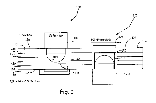
[0010] FIG. 1 is a diagrammatic view of a pair of optocouplers in
accordance with an
embodiment of the present invention. Optocoupler 100 is formed by photoemitter
102 and
photodetector 104 arranged on opposite sides of printed circuit board 106. In
the embodiment
illustrated in FIG. 1, photoemitter 102 is an infrared photo diode having a
hemispherical portion
108 that is received within bore 110 in printed circuit board 106.
Additionally, in this
embodiment, photodetector 104 is a PIN diode. This arrangement could be
considered to show a
pair of cooperative photoelements where at least one of the photoelements (in
this case the
photoemitter) has an active surface that is at least partially disposed in a
recess of printed circuit
board 106. In accordance with one embodiment of the present invention, bore or
recess 110 ends
in surface 112 and the sidewalls of recess 110 preferably meet surface 112 at
approximately 90
degrees. Surface 112 is spaced from surface 114 of printed circuit board 106
by at least 0.2 mm,
which is the minimum requirement of solid material in order to comply with
60079-11 appendix
F for 300V. Photodetector 104 is mounted adjacent surface 114 such that light
emitted from
photoemitter 102, which passes through surface 112, is detected by
photodetector 104. In this
way, emitter 102 and detector 104 cooperate to form an optocoupler. As can be
appreciated, the
arrangement of photoemitter 102 and photodetector 104 provide signal
communication in a
single direction (from photoemitter to photodetector). Thus, in order to
provide bi-directional
communication across printed circuit board 106, a second optocoupler 121 is
provided which is
substantially the reverse of optocoupler 100. Specifically, optocoupler 121
includes photoemitter
116 extending into bore or recess 118 within printed circuit board 106. Recess
118 terminates in
surface 120 that is spaced from surface 122 of printed circuit board 106 by
the minimum solid
insulation dimension (0.2 mm). Photodetector 124, in one embodiment, is
mounted adjacent
surface 122 such that light passing through surface 120 is detected by
photodetector 124. Thus,
photoemitter 116 and photodetector 124 comprise a second optocoupler that, in
cooperation with
optocoupler 100, provides bi-directional communication through print circuit
board 106.
[0011] FIG. 1 illustrates printed circuit board 106 having six different
copper layers 126,
128, 130, 132, 134 and 136, which are separated by printed circuit board (PCB)
material 119 and
held back or otherwise spaced from recesses 110, 118 by the minimum solid
material spacing in
accordance with 60079-11, appendix F. Specifically, in the embodiment
illustrated in FIG. 1, that
CA 02923172 2016-03-03
WO 2015/047619 PCT/US2014/052467
4
spacing is 0.2 mm minimum. Photoemitter 102 extends into recess 110 such that
the dome 108 of
photoemitter 102 is proximate surface 112. Such proximity increases the signal
to noise ratio of
optocoupler 100 and allows the overall power to be reduced. While embodiments
of the present
invention are generally described with a portion of the photoemitter being
disposed in the recess
of the printed circuit board, it is expressly contemplated that the
photodetector could be disposed
in a recess instead or as well. However, in all such configurations, at least
one active surface
(dome of the photoemitter or detecting interface of the photodetector) is
disposed within a recess
of the printed circuit board.
[0012] When properly aligned, the photodetector will receive the signal
from the
photoemitter that is located directly opposite it. In one embodiment, the
photodetector has its
active surface aligned with the center of the photoemitter' s dome (such as
dome 108).
[0013] FIG. 2 is a diagrammatic view of a preferred method of generating
recesses 110, 118.
Typically, a bore is generated with a drill bit, such as drill bit 150 which
has a tapered end 152
resulting in a tapered end surface 154. However, tapered end surface 154 will
actually bend or
otherwise refract electromagnetic spectrum passing through this interface.
Thus, the
electromagnetic signal 156 is diffused and the electrical response of
photodetector die 158 is
attenuated. In a preferred embodiment, a flat bottom bit 160 is employed. Bit
160 has an end 162
that is substantially flat. This results in a bore 164 having an end 166 that
is at approximately a
right angle to the sidewall of bore 164. Flat surface 166 ensures that the
signal passing through
this air to circuit board interface maintains its original direction and is
not refracted or otherwise
affected. In this way, signal 168 passes straight through to photodetector die
170, which has a
larger response in comparison to photodetector die 158. In another example
configuration, the
drill bit has a concave shaped end.
[0014] Several methods may be employed in accordance with embodiments of
the present
invention to reduce signal attenuation due to the printed circuit board
material and other factors.
Specifically, printed circuit board material can be removed while leaving
enough material to
satisfy the spacing requirements when considering manufacturing tolerances.
Further, the
photoemitter and photodetector components can be selected for signal strength
and optical scatter
pattern. Further, a solder mask between the active surfaces of the optical
components can be
omitted. Finally, as set forth above with respect to FIG. 2, the use of a flat-
nosed drill bit for
generating the counter bore can be employed. Any or all of these various
design considerations
CA 02923172 2016-03-03
WO 2015/047619 PCT/US2014/052467
cooperate to provide a optocoupler formed of a plurality of discrete
components that complies
with intrinsic safety specifications very effectively while maintaining a
small printed circuit
board footprint.
[0015] As can be appreciated, forming adjacent optocouplers in order to
provide isolated bi-
directional communication through printed circuit board 106 using discrete
components can
generate crosstalk between the optocouplers, if unwanted or stray signals are
not carefully
inhibited. There are two primary ways in which crosstalk can be present. FIG.
3 illustrates these
two primary crosstalk channels. The first crosstalk channel is along the board
surface as
illustrated by dashed line 180. In this case, infrared illumination from
photoemitter 102 is able to
pass directly along board surface 122 to photodetector 124. This first form of
crosstalk can be
reduced by increasing the space between photoemitter 102 and photodetector
124. However,
increasing the space between these components is not desired since that will
consume valuable
printed circuit board space. A more favored solution is to add an opaque cover
over
photodetector 124 such that it cannot receive crosstalk illumination 180. One
preferred form of
such an opaque cover is opaque potting provided around and/or over
photodetector 124. This
opaque potting has the added benefit of eliminating the effects of ambient
light on photodetector
124. Example materials include epoxy or silicone RTV.
[0016] The second channel of crosstalk illustrated in FIG. 3 is shown at
reference numeral
182. Specifically, this crosstalk channel is generated by infrared
illumination passing within the
material of printed circuit board 106. This crosstalk can be reduced by
placing copper layers 126,
128, 130, 132, 134, 136 closer together to force the light to diffuse more
rapidly when traveling
through the board. Further, placing the copper layers closer to the
photoemitter recess reduces
the amount of signal that scatters away from the photodetector. This reduces
the size of the
opening through the copper layers and thereby blocks crosstalk channel 182.
Additionally, the
interior wall of the recess can be treated to facilitate signal transmission
from the photoemitter to
the photodetector and/or treated to reduce cross talk. For example, a sleeve
can be inserted about
the dome of the emitter or the recess itself can be coated or otherwise
treated with a material to
facilitate signal transmission.
[0017] Embodiments of the present invention generally provide a highly
compact
optocoupler arrangement that can easily satisfy intrinsic safety
specifications for field devices
CA 02923172 2016-03-03
WO 2015/047619 PCT/US2014/052467
6
and other electronics. It is believed that the optocouplers in accordance with
embodiments of the
present invention can provide signal coupling at 125 kHz, and possibly as high
as 250 kHz.
[0018] Embodiments of the present invention can be used in any electronic
device where
optocouplers are warranted. However, embodiments of the present invention are
particularly
useful for field devices that must comply within an intrinsic safety
specification, such as that set
forth above.
[0019] Although the present invention has been described with reference to
preferred
embodiments, workers skilled in the art will recognize that changes may be
made in form and
detail without departing from the spirit and scope of the invention. The above
discussion refers to
a solid separation of 0.2 mm between the optical components. Although such a
configuration is
specifically directed to providing isolation between an intrinsically safe
region to an non-
intrinsically safe region, the invention is not limited to this configuration.
The same isolation
distance can be used to isolate intrinsically safe sections from one another.
Similarly, the amount
of separation may be more or less than 0.2 mm depending upon isolation
requirements and
design constraints. The invention is applicable to electromagnetic radiation
of any frequency
including visible light, infrared and ultraviolet radiation. A translucent
filler medium can be
applied between the photo emitter and the printed circuit card to reduce
attenuation due to
refraction and reflection between the different medium layers.