Note: Descriptions are shown in the official language in which they were submitted.
DEVICE AND METHOD FOR CURRENT FLOW CONTROL FOR
DUAL BATTERY VEHICLE ARCHITECTURE
[0001]
FIELD OF INVENTION
[0002] This application is related to vehicle electronics.
BACKGROUND
[0003] Some vehicles now have stop-start systems that automatically limit
idling in a motionless vehicle. In particular, when the vehicle comes to a
stop,
the engine computer or control unit stops sparking and providing fuel. When
the
driver lifts his or her foot off the brake, or engages the clutch, the engine
fires
back up. In these stop-start situations, current is drawn from the overall
vehicle
electrical systems when re-cranking the vehicle through the main battery and
starter circuit. This may cause brown out conditions with respect to the
overall
vehicle electrical systems, such as the radio, navigation and or other vehicle
electrical systems.
SUMMARY
[0004] Described herein is a device and method for current flow control
for
dual battery vehicle architecture. The dual battery vehicle architecture
includes
a second energy source that is used to support electrical loads, such as radio
and
navigation systems, during re-cranking in stop-start situations. A quasi-diode
device is configured to effectively split a main battery and starter circuit
from the
rest of the vehicle electrical system including the second energy source. The
quasi-diode device includes a plurality of field effect transistors (FET) that
-1-
Date Recue/Date Received 2020-11-20
CA 02924798 2016-03-18
WO 2015/041749
PCT/US2014/048631
conducts current in both directions between the main battery and starter
circuit
and the rest of the vehicle electrical system when the FETs are turned on and
conducts current only from the main battery and starter circuit to the rest of
the
vehicle electrical system when the FETs are turned off, i.e. when re-cranking
is
occurring during a start-stop situation.
BRIEF DESCRIPTION OF THE DRAWINGS
[0005] Figure 1 shows an example dual battery vehicle architecture and
circuit in accordance with one or more disclosed embodiments;
[0006] Figure 2 shows an example high level block diagram of a quasi-diode
device in accordance with one or more disclosed embodiments;
[0007] Figure 3 shows an example circuit diagram of a quasi-diode device
in accordance with one or more disclosed embodiments;
[0008] Figure 4 shows an example schematic for a quasi-diode device in
accordance with one or more disclosed embodiments;
[0009] Figure 5 shows an example view of a quasi-diode device in
accordance with one or more disclosed embodiments;
[0010] Figure 6 shows an example perspective view of a quasi-diode device
in accordance with one or more disclosed embodiments;
[0011] Figure 7 shows an example internal view of a quasi-diode device in
accordance with one or more disclosed embodiments;
[0012] Figure 8 shows an example view of a quasi-diode device in
accordance with one or more disclosed embodiments with outer casing removed;
and
[0013] Figure 9 shows an example view of a quasi-diode device in
accordance with one or more disclosed embodiments with outer casing and cover
removed.
DETAILED DESCRIPTION
[0014] It is to be understood that the figures and descriptions of
embodiments of the quasi-diode device and associated circuitry have been
-2-
CA 02924798 2016-03-18
WO 2015/041749
PCT/US2014/048631
simplified to illustrate elements that are relevant for a clear understanding,
while eliminating, for the purpose of clarity, many other elements found in
typical technology. Those of ordinary skill in the art may recognize that
other
elements and/or steps are desirable and/or required in implementing the quasi-
diode device and associated circuitry. However, because such elements and
steps
are well known in the art, and because they do not facilitate a better
understanding of the quasi diode device and associated circuitry, a discussion
of
such elements and steps is not provided herein.
[0015] The non-limiting embodiments described herein are with respect to
the quasi diode device and associated circuitry. The embodiments and
variations
described herein, and/or shown in the drawings, are presented by way of
example
only and are not limiting as to the scope and spirit. The quasi diode device
and
associated circuitry may be used in a number of applications.
[0016] In general, in a dual battery vehicle architecture or system, a
quasi-
diode device is configured to effectively split a main battery and starter
circuit
from the rest of the vehicle electrical system including a second energy
source.
The quasi-diode device includes a plurality of field effect transistors (FET)
that
conducts current in both directions between the main battery and starter
circuit
and the rest of the vehicle electrical system when the FETs are turned on and
conducts current only from the main battery and starter circuit to the rest of
the
vehicle electrical system when the FETs are turned off, i.e. when re-cranking
is
occurring during a start-stop situation. The quasi-diode device limits the
voltage
drop at the second energy source during re-cranking and prevents current from
being drawn from the overall electrical system to the main battery and starter
circuit.
[0017] In comparison to a simple semiconductor diode, the quasi-diode
device uses FETs to conduct current and therefore has lower voltage drops and
less power losses, which eliminate the need for costly heat sinking. In
addition,
as compared to an electromechanical solution, (such as a relay), the quasi-
diode
device offers higher life cycles and noiseless operation.
-3-
CA 02924798 2016-03-18
WO 2015/041749
PCT/US2014/048631
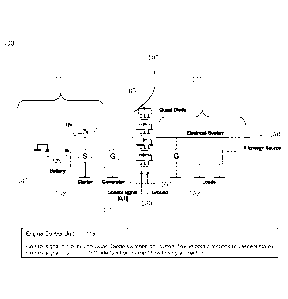
[0018] Figure 1 shows an example dual cell system 100 using a quasi-diode
device 105 connected between a main battery and starter circuit 110 and a
remaining vehicle electrical system 115. The main battery and starter circuit
110 includes at least a battery 140 and a starter 142. The remaining vehicle
electrical system 115 includes at least a second energy source 150 and loads
152.
A generator 160 may be part of the main battery and starter circuit 110 or the
remaining vehicle electrical system 115, depending on vehicle system
implementation.
[0019] The quasi-diode device 105 includes four (4) N-channel FETs 107
that are connected in parallel. Although N-channel FETs are used in the
description herein of the quasi-diode device, P-channel FETs may also be used
without deviating from the scope of the invention described herein. The quasi-
diode device 105 has an enable control signal 170 provided by an engine
control
unit 175 for turning or switching the quasi-diode device 105 on or off in
accordance with engine re-start conditions. In a diode emulation mode, when
the
enable control signal 170 is low, the quasi-diode device 105 is off and
current
flows from the main battery and starter circuit 110 to the remaining vehicle
electrical system 115. In an ON state, when the enable control signal 170 is
high
or not connected, the quasi-diode device 105 is on and current flows in both
directions between the main battery and starter circuit 110 and the remaining
vehicle electrical system 115. Although the quasi-diode device 105 is
described
herein below with respect to an active low enable control signal, an active
high
enable control signal may be used without deviating from the scope of the
invention described herein. As further described herein below, during
cranking,
no current is nominally flowing through the quasi-diode device while the
voltage
at the main battery and starter circuit 110 is lower than the remaining
vehicle
electrical system 115. A ground path 180 is provided for the dual cell system
100.
[0020] In an embodiment, the quasi-diode device 105 may be implemented
by 4 OptiMOSTm N-channel 0.9mS2 transistors connected in parallel,
(OptilVIOSTm
is a trademark of Infineon Technologies), where illustrative operating
characteristics and/or features are noted in Table 1.
-4-
CA 02924798 2016-03-18
WO 2015/041749 PCT/US2014/048631
= 4 OptiMOS N-channel 0.9m0 transistors connected in parallel
= Operating temperature range: -40 C ... 105 C
= Maximum continuous Load Current:
o 200A @ Ta = 25 C
o 160A @ Ta = 105 C
= Maximum Body Diode conduction current:
o 50A @ Ta = 25 C
o 20A @ Ta = 105 C
= Increase in Tj during transient peak current (if the application requires
the QD to be
ON during cold crank): 45 C maximum
= Quiescent Current Consumption: 280pA ¨ measured @ 12V & 25 C (QD ON
state)
= Current Consumption Diode Emulation state = 4.38mA - measured @ 12V & 25
C
= QDiode Ron: ¨330p0 ¨ measured @ Ta = 25 C
= Short to ground protection:
o Starter side ¨ YES: QD turns/stays off if V_BAT goes below V_BN/2 -
adjustable.
o Boardnet side ¨ NO (due to direct conduction through the body diodes)
Note: The numbers shown above are illustrative and are for purposes of example
only.
Table 1
[0021] Figure 2 shows a high level block diagram of a quasi-diode module
200 that has four input signals: 1) an enable control signal, EN_Q, which is
the
quasi-diode device 200 control signal and in this illustrative embodiment, is
active low; 2) a ground path, GND; 3) a battery current connection, BATT; and
4)
a remaining vehicle electrical system current connection, which is also known
as
boardnet, BN. The quasi-diode module 200 includes a filtering module 205
connected to a boost converter module 210, a protection module 215 connected
to
the boost converter module 210 and a fast gate discharge 220 via an AND logic
gate 225. The boost converter module 210 is further connected to a quasi-diode
device 230. The quasi-device diode 230 includes a plurality of FETs 235 that
are
connected in parallel.
[0022] The BATT is connected to a source (3) of each of the plurality of
FETs 235 and the BN is connected to a drain (2) of each of the plurality of
FETs
235. The BATT and BN are also connected to the filtering module 205 and the
protection module 215. The control signal EN_Q and the output of the
protection
module 215 are connected to the AND logic gate 225. The output of the AND
logic gate 225, control signal shutdown (SHDN), is connected to the boost
converter module 210 and the fast gate discharge 220. The outputs of the boost
converter module 210 and the fast gate discharge 220 are connected to a gate
(1)
-5-
CA 02924798 2016-03-18
WO 2015/041749
PCT/US2014/048631
of each of the plurality of FETs 235. In an embodiment, as further described
herein below, the quasi-diode device 230 may be implemented on a power board
240 and the filtering module 205, the protection module 215, the boost
converter
module 210, fast gate discharge module 220 and the AND logic gate may be
implemented on a control board 245.
[0023] Operationally, the filtering module 205 performs standard
filtering,
and overvoltage, overcurrent and reverse battery protection with respect to
BATT
and BN. To turn the quasi-diode device 230 on, the control signal EN_Q is high
or
not connected and the gate voltage must be greater than the source voltage,
which as described herein above is tied to BATT. This is accomplished by the
boost converter module 210, which takes the voltage coming out of the
filtering
module 205 and boosts the voltage by a predetermined voltage. This boosted
voltage then becomes the gate voltage. In an embodiment, the predetermined
voltage is ten (10) volts.
[0024] The quasi-diode device 230 may be in one of three modes or states,
an ON-state, a diode emulation state or a short circuit state. In the diode
emulation state, the control signal EN_Q signal is low, the control signal
SHDN
is active and the boost converter module 210 is inactive or off. Consequently,
the
quasi-diode device 230 is off. In this mode, the plurality of FETs 235
emulates
ideal diode function, that is, current is only allowed to flow from the main
battery
and starter circuit 110 to the remaining vehicle electrical system 115 as
shown in
Figure 1.
[0025] In the ON-state, the control signal EN_Q is high or not connected
(NC), and the quasi-diode device 230 is in an ON-state as long as the BATT
voltage is higher than a predetermined value of the BN. Once a short circuit
condition is detected while the control signal EN Q is high or not connected
and
the BN voltage becomes higher than the BATT voltage, then the quasi-diode
device 230 switches from an ON-state to a short circuit state in order to
protect
itself from being damaged. In the short circuit state, the FETs 235 are
switched-
off. The quasi-diode device 230 resides in this state until the short-circuit
situation is rectified. In an embodiment, the short circuit threshold is when
the
-6-
CA 02924798 2016-03-18
WO 2015/041749
PCT/US2014/048631
BATT voltage is equal to or higher than half the BN voltage. The short circuit
functionality is implemented by the protection module 215, which causes the
control signal SHDN to be low in the event of a short circuit. As shown in
Figure
3, the short circuit threshold can be set up by a resistive divider ratio at
the input
of a comparator circuit in an example embodiment. Short circuits to ground are
detected only at the main battery and starter circuit 110 (BATT) as shown in
Figure 1. A short circuit (to ground) detection at the remaining vehicle
electrical
system 115 (BN) is rendered ineffective by the fact that current flow in the
BN
direction cannot be blocked.
[0026] In the event of a short circuit, the power in the quasi-diode
device
230 must be dissipated quickly or the FETs 235 may be damaged. This is
implemented by the fast gate discharge module 220, which establishes a path to
ground when the control signal SHDN is low.
[0027] Figure 3 shows an example circuit diagram for a quasi-diode module
300 including example circuits for a filtering circuit 305, a boost converter
circuit
307, a protection circuit 309 and a fast gate discharge circuit 311. The
control
signal EN_Q is pulled up with 10k resistor 302 through a protection diode 304.
[0028] The filtering circuit 305 has a battery current connection, BATT,
tied to a capacitor circuit 315 and a diode 317, and a boardnet current
connection,
BN, tied to a capacitor circuit 320 and a diode 321. The capacitor circuit 315
and
capacitor circuit 320 provide electromagnetic interference (EMI) filtering and
electrostatic discharge (ESD) protection. The diodes 317 and 321 provide
reverse
battery protection. The outputs of the diodes 317 and 321 are tied together at
a
node B+. The capacitor circuit 322 provides further EMI filtering. The node B+
represents a voltage net and is the supply voltage after the reverse polarity
protection. The B+ node is connected to a current limiting resistor 325, which
provides overcurrent protection. The other end of current limiting resistor
325 is
connected to a circuit 327 which provides over-voltage protection.
[0029] The boost converter circuit 307 uses a switch mode step-up circuit
340 which has a VIN pin connected to the output of the filtering circuit 305
and a
SHDN pin connected to an output of the protection circuit 309 and the control
-7-
signal EN_Q. The switch mode step-up circuit 340 is, for example, a micropower
step-up DC/DC converter. The output of the boost converter circuit 307 is set
by
resistor 342, transistor 344 and resistor 346 to VIN + 10V. The voltage
offset, i.e.
1011 in this example, can be set by changing the values of resistor 342,
transistor
344 and resistor 346.
[0030] The protection circuit 309 includes a conventionally configured
comparator circuit 350 which has BATT and BN connected as inputs via resistor
network circuits 352 and 354, respectively. As described herein above, the
resistor network circuits 352 and 354 can be configured to establish the short
circuit threshold. The output of the protection circuit 309 is connected to
the
switch mode step-up circuit 340 and to the fast gate discharge circuit 311.
[0031] The fast gate discharge circuit 311 has two (2) N-channel FETs 360
and 362, respectively, which provide a path to ground in the event of a short
circuit, i.e. when control signal SHDN is low and active. The purpose of the
fast
gate discharge circuit 311 is to turn off the 4 FETs, e.g. the plurality of
FETs 235
in Figure 2, very fast. This is accomplished by providing a path to discharge
to
ground the 4 FETs gate charge. As described herein above, this happens when
the quasi-diode device is on. This fast discharge is activated at the same
time
with turning the boost converter circuit 307 off, (i.e. pulling SHDN low), and
is
done either by EN _Q going low or in case of short circuit when the protection
circuit 309 is triggered.
[0032] Figures 4A, 4B and 4C show example packaging schematic diagrams
for a quasi-diode module 400 in accordance with one or more disclosed
embodiments. In particular, Figure 4A shows a direct view of a BN connector
405, a BATT connector 410, and connector port 412 including a ground pin 415
and a control signal EN _Q pin 420. Figure 4B shows a bottom view of the quasi-
diode module 400 including a view of a rubber grommet 430 for environmental
sealing and a heat sink 440. Figure 4C shows a side view of the BN connector
405
and the connector port 412.
[0033] Figure 5 shows an example view of a quasi-diode module 500 in
accordance with one or more disclosed embodiments. In particular, a housing or
-8-
Date Recue/Date Received 2020-11-20
CA 02924798 2016-03-18
WO 2015/041749
PCT/US2014/048631
enclosure 505 is shown with a BN connector 510, a BATT connector 515, and
connector port 520.
[0034] Figure 6 shows an example perspective view of a quasi-diode module
600 in accordance with one or more disclosed embodiments and in particular, a
bottom view of the embodiment shown in Figure 5. A BN connector 610, a BATT
connector 615, a connector port 620 and a heat sink 625 are shown.
[0035] Figure 7 shows an example internal view of a quasi-diode module
700 in accordance with one or more disclosed embodiments with a front surface
or wall removed. This view of the a quasi-diode module 700 shows a BN
connector 710, a BATT connector 715, a ground pin 720, a EN_Q pin 725, a
control board 730, a heat sink 735, a thermal pad 740, a rubber grommet 745,
and a power board 750.
[0036] Figure 8 shows an example view of a quasi-diode module 800 in
accordance with one or more disclosed embodiments with an outer casing
removed. This view of the a quasi-diode module 800 shows a BN connector 810, a
BATT connector 815, a ground pin 820, a EN_Q pin 825, a control board 830, a
heat sink 835, a thermal pad 840, a rubber grommet 845, a power board 850, a
BN connector 855, a BATT connector 860 and an output voltage (for a gate of
the
FETs) connector 865.
[0037] Figure 9 shows an example view of a quasi-diode module 900 in
accordance with one or more disclosed embodiments with outer casing and a
control board removed. This view of the a quasi-diode module 900 shows a BN
connector 910, a BATT connector 915, a heat sink 935, a thermal pad 940, a
rubber grommet 945, a power board 950, a BN connector 955, a BATT connector
960, an output voltage (for a gate of the FETs) connector 965 and FETs 970.
[0038] Although features and elements are described above in particular
combinations, each feature or element can be used alone without the other
features and elements or in various combinations with or without other
features
and elements.
-9-