Note: Descriptions are shown in the official language in which they were submitted.
CA 02927030 2016-04-12
1
[Document Name] Description
[Title of Invention] LED DRIVER CIRCUIT
[Technical Field]
[0001]
The present invention relates to an LED driver circuit.
[Background Art]
[0002]
There is an input circuit detects the on/off state of a switch
device used by a user to operate a headlamp or a turn signal of an
automobile or a motorcycle. To prevent erroneous detection of the
on/off state of the switch device caused by a leak current when the
switch device is wetted with water, the conventional input circuit is
designed to pass the leak current to the ground.
[0003]
In particular, the switch device for a headlamp or a turn
signal of a motorcycle is more likely to be wetted with water, and
the leak current tends to be greater, because of the structure of the
motorcycle. To
prevent erroneous detection and erroneous
lighting caused by the leak current, the conventional input circuit
has elaborate wiring designed for passing the leak current to the
lamp, for example.
[0004]
As conventional techniques using an LED lamp as a light,
there are a technique that involves a resistor connected in parallel
with the LED (see Japanese Patent Laid-Open No. 2003-63305, for
example), a technique that involves detecting the on/off state of
the switch device while switching (see Japanese Patent Laid-Open
No. 2013-33610), a technique that involves a constant current
circuit (see Japanese Patent Laid-Open No. 2014-40142), and a
technique that involves using a magnet and a Hall device (see
National Publication of International Patent Application No. 2014-
531715, for example).
= CA 02927030 2016-04-12
-
2
[Summary of Invention]
[Technical Problem]
[0005]
However, the conventional techniques have problem of
5 heating of the resistor or the constant current circuit, adjustment
of the sampling timing, or increase of the cost as a result of using
the magnet or Hall device, for example.
[0006]
In view of such circumstances, an object of the present
10 invention is to provide an LED driver device that is an input circuit
that detects the on/off state of a switch device used by a user to
operate an LED lamp in a headlamp, a turn signal or the like, the
LED driver device being able to be manufactured at reduced cost
and to prevent erroneous detection of the on/off state of the switch
15 device caused by a leak current when the switch device is wetted
with water.
[Solution to Problem]
[0007]
An LED driver circuit according to an embodiment of an
20 aspect of the present invention controls driving of an LED lamp in
response to an on/off state of a mechanical switch device,
comprising:
a first terminal to which a current path of the switch device
is connected at one end thereof;
a second terminal to which the current path of the switch
device is connected at another end thereof, the switch device and a
battery being connected in series between the first terminal and
the second terminal;
a detection circuit that periodically detects a current flowing
to the first terminal and outputs a detection signal responsive to a
result of the detection at a first node;
a comparison circuit that compares a detection voltage
responsive to the detection signal with a threshold voltage and
outputs a comparison result signal responsive to a result of the
comparison; and
a control circuit that controls a current detection operation
= CA 02927030 2016-04-12
3
of the detection circuit and controls driving of the LED lamp based
on the comparison result signal,
wherein the control circuit determines that the switch device
is in an on state and the current path is conductive between the
one end and the another end if the comparison result signal
indicates that the detection voltage is equal to or higher than the
threshold voltage, and
determines that the switch device is in an off state and the
current path is interrupted between the one end and the another
end if the comparison result signal indicates that the detection
voltage is lower than the threshold voltage,
wherein the detection circuit comprises:
a first switch element that is connected to the first terminal
at one end thereof and is turned on and off under the control of the
control circuit;
a detection capacitor that is connected to another end of the
first switch element at one end thereof and to the first node at
another end thereof;
a detection resistor that is connected to the first node at one
end thereof and to the second terminal at another end thereof; and
a discharge resistor that is connected in parallel with the
detection resistor and the detection capacitor between another end
of the first switch element and the second terminal, the discharge
resistor being connected to the another end of the first switch
element at one end thereof and to the second terminal at another
end thereof,
the control circuit
controls the first switch element to periodically switch on
and off, and
the detection circuit
outputs the detection signal at the first node.
[0008]
[0009]
In the LED driver circuit, wherein the detection circuit
further comprises:
CA 02927030 2016-04-12
4
a second switch element that is connected in series with the
discharge resistor between the another end of the first switch
element and the second terminal, and
the control circuit
controls the second switch element to switch off when the
control circuit turns on the first switch element, and
controls the second switch element to switch on when the
control circuit turns off the first switch element.
[00010]
The LED driver circuit further comprising:
a peak hold circuit that holds a peak voltage of the detection
signal and outputs the held peak voltage as the detection voltage
at a second node.
[00011]
In the LED driver circuit, wherein the peak hold circuit
comprises:
a holding diode that is connected to the first node at an
anode thereof and to the second node at a cathode thereof; and
a holding capacitor that is connected between the second
node and the second terminal.
[00012]
In the LED driver circuit, wherein the comparison circuit
comprises:
a voltage divider circuit that outputs a divided voltage as
the threshold voltage, the divided voltage being obtained by
dividing a voltage between the first terminal and the second
terminal; and
a comparator that receives the detection voltage and the
threshold voltage, compares the detection voltage with the
threshold voltage, and outputs the comparison result signal in
response to a result of the comparison.
[00013]
In the LED driver circuit, wherein the voltage divider circuit
comprises:
a first voltage divider resistor that is connected to the first
terminal at one end thereof and to a voltage dividing node at
CA 02927030 2016-04-12
another end thereof; and
a second voltage divider resistor that is connected to the
voltage dividing node at one end thereof and to the second
terminal at another end thereof, and
5 the
voltage divider circuit outputs a voltage at the voltage
dividing node as the threshold voltage.
[0014]
In the LED driver circuit, wherein the threshold voltage is
set to be higher than the detection voltage, which is the peak
voltage of the detection signal that is output from the detection
circuit as a result of the control circuit periodically turning on and
off the first switch element, in a state where the switch device is in
the off state and a leak current is flowing in the current path.
[0015]
In the LED driver circuit, wherein the threshold voltage is
set to be lower than the detection voltage, which is the peak
voltage of the detection signal that is output from the detection
circuit as a result of the control circuit periodically turning on and
off the first switch element, in a state where the switch device is in
the on state.
[0016]
In the LED driver circuit, wherein the switch device and the
battery are connected in series between the first terminal and the
second terminal, the battery being connected to the first terminal
on the side of a positive electrode thereof and to the second
terminal on the side of a negative electrode thereof.
[0017]
In the LED driver circuit, wherein the detecting capacitor
has a capacitance greater than a capacitance of the holding
capacitor.
[0018]
In the LED driver circuit, wherein a leak current flows in the
current path of the switch device despite the switch device being in
the off state when the switch device is wetted with water.
[0019]
In the LED driver circuit, wherein the LED driver circuit is
CA 02927030 2016-04-12
=
. .
6
mounted on a motorcycle,
the LED lamp is a headlamp or a turn signal of the
motorcycle, and
the switch device is a handle switch of the motorcycle that is
manipulated by a user to control driving of the LED lamp.
[0020]
The LED driver circuit, further comprising:
a power supply circuit that is connected to the first terminal
and supplies electric power to the control circuit based on a current
input from the first terminal,
the power supply circuit operates on the current input from
the first terminal and supplies electric power to the control circuit
based on the current input from the first terminal when the switch
device is in the on state or when the switch devices is in the off
state and a leak current flows in the current path, and
the control circuit operates on the electric power supplied
from the power supply circuit and drives the LED lamp.
[0021]
In the LED driver circuit, wherein the first switch element is
a pMOS transistor that is connected to the first terminal at a source
thereof and to the one end of the detection capacitor at a drain
thereof and has a gate voltage controlled by the control circuit.
[0022]
An LED driver circuit according to an aspect of the present
invention is an LED driver circuit that controls driving of an LED
lamp in response to an on/off state of a mechanical switch device,
and the LED driver circuit includes: a first terminal to which a
current path of the switch device is connected at one end thereof;
a second terminal to which the current path of the switch device is
connected at another end thereof, the switch device and a battery
being connected in series between the first terminal and the second
terminal; a detection circuit that periodically detects a current
flowing to the first terminal and outputs a detection signal
responsive to a result of the detection at a first node; a comparison
circuit that compares a detection voltage responsive to the
detection signal with a threshold voltage and outputs a comparison
CA 02927030 2016-04-12
7
result signal responsive to a result of the comparison; and a control
circuit that controls a current detection operation of the detection
circuit and controls driving of the LED lamp based on the
comparison result signal.
[0023]
The control circuit determines that the switch device is in an
on state and the current path is conductive between the one end
and the another end if the comparison result signal indicates that
the detection voltage is equal to or higher than the threshold
voltage, and determines that the switch device is in an off state
and the current path is interrupted between the one end and the
another end if the comparison result signal indicates that the
detection voltage is lower than the threshold voltage.
[0024]
In this way, the LED driver circuit can detect the on/off state
of the switch device even if the switch device is wetted with water
and a leak current occurs.
[0025]
The LED driver circuit according to the present invention
does not require adjustment of the detection timing nor any
expensive element, such as a Hall device. In addition, the LED
driver circuit according to the present invention can be used with a
relatively cheap mechanical switch device (such as a switch device
with low waterproofness), and the cost can be reduced.
[0026]
In short, the LED driver circuit according to the present
invention can be manufactured with reduced cost and can reduce
the possibility of erroneous detection of the on/off state of the
switch device caused by a leak current when the switch device is
wetted with water.
[Brief Description of Drawings]
[0027]
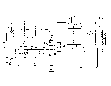
[Figure 1] Figure 1 is a diagram showing an example of a
configuration of an LED driver system 1000 according to a first
embodiment.
[Figure 2] Figure 2 is a waveform diagram showing an
CA 02927030 2016-04-12
=
8
example of operation waveforms of an LED driver circuit 100 shown
in Figure 1.
[Figure 3] Figure 3 is a waveform diagram showing another
example of operation waveforms of the LED driver circuit 100
shown in Figure 1.
[Figure 4] Figure 4 is a diagram showing an example of a
configuration of an LED driver system 2000 according to a second
embodiment.
[Description of Embodiments]
[0028]
Embodiments of the present invention will be described with
reference to the drawings.
[0029]
(First Embodiment)
An LED driver system 1000 (Figure 1) according to a first
embodiment includes a battery "B", a mechanical switch device
"SW" connected to the battery "B", an LED lamp 101 and an LED
driver circuit 100 that controls driving of the LED lamp 101 in
response to the on/off state of the mechanical switch device "SW".
[0030]
The LED driver system 1000 is mounted on a motorcycle,
for example. In that case, the LED lamp 101 is a headlamp or a
turn signal of the motorcycle, for example. Furthermore, in that
case, the switch device "SW" is a handle switch of the motorcycle
that is manipulated by the user for controlling driving of the LED
lamp 101.
[0031]
If the mechanical switch device "SW" is wetted with water,
for example, a leak current flows in a current path of the switch
device "SW" even if the switch device "SW" is in the off state.
[0032]
The LED driver circuit 100 includes a first terminal "Ti", to
which the current path of the switch device "SW" is connected at
one end thereof, and a second terminal "T2", to which the current
path of the switch device "SW" is connected at another end thereof
(Figure 1).
CA 02927030 2016-04-12
. ,
9
[0033]
The switch device "SW" and the battery "B" are connected in
series between the first terminal "TV' and the second terminal "T2".
In the example shown in Figure 1, the current path of the switch
device "SW" is connected to the first terminal "Ti" at one end
thereof and to a positive electrode of the battery "B" at another
end thereof, and the battery "B" is connected to the second
terminal "T2" at a negative electrode thereof.
[0034]
That is, the switch device "SW" and the battery "B" are
connected in series between the first terminal "Ti" and the second
terminal "T2" in such a manner that the battery "B" is connected to
the first terminal "Ti" on the side of the positive electrode and to
the second terminal "T2" on the side of the negative electrode.
[0035]
In the example shown in Figure 1, the second terminal "T2"
is grounded.
[0036]
The LED driver circuit 100 includes a detection circuit "DC"
that periodically detects the current flowing to the first terminal
"Ti" and outputs a detection signal "SX" responsive to the
detection result at a first node "Ni". The LED driver circuit 100
further includes a comparison circuit "CC" that compares a
detection voltage "VZ" responsive to the detection signal "SX" with
a threshold voltage "Vth" and outputs a comparison result signal
"So" responsive to the comparison result.
[0037]
The LED driver circuit 100 further includes a peak hold
circuit "HC" that holds a peak voltage of the detection signal "SX"
and outputs the held peak voltage as the detection voltage "VZ" at
a second node "N2". The LED driver circuit 100 further includes a
control circuit "CON" that controls the current detection operation
of the detection circuit "DC" and controls driving of the LED lamp
101 based on the comparison result signal "So".
[0038]
The LED driver circuit 100 further includes a power supply
CA 02927030 2016-04-12
circuit "SC" that is connected to the first terminal "Ti" and supplies
electric power to the control circuit "CON" based on a current input
from the first terminal "Ti".
[0039]
5 In the
example shown in Figure 1, the detection circuit "DC"
includes a first switch element "Q1" that is connected to the first
terminal "Ti" at one end thereof and is turned on and off under the
control of the control circuit "CON", and a detection capacitor "CX"
that is connected to another end of the first switch element "Q1" at
10 one end thereof and to the first node "Ni" at another end thereof.
[0040]
The detection circuit "DC" further includes a detection
resistor "RX" that is connected to the first node "Ni" at one end
thereof and to the second terminal "T2" at another end thereof,
and a discharge resistor "RY" that is connected to the another end
of the first switch element "Q1" at one end thereof and to the
second terminal "T2" at another end thereof.
[0041]
As shown in Figure 1, the first switch element "Q1" is a
pMOS transistor that is connected to the first terminal "Ti" at a
source thereof and to the one end of the detection capacitor "CX"
at a drain thereof, for example. A gate voltage of the pMOS
transistor is controlled by a control signal (a gate signal "SG1"
output from a pre-driver circuit "PC") output from the control
circuit "CON". That is, the pMOS transistor is turned on and off
under the control of the gate signal "SG1".
[0042]
The detection resistor "RX" is a resistor for detecting a
current "IX" that flows to the detection capacitor "CX".
[0043]
The discharge resistor "RY" is connected in parallel with the
detection resistor "RX" and the detection capacitor "CX" between
the another end of the first switch element "Q1" and the second
terminal "T2". The
discharge resistor "RY" is a resistor for
discharging the detection capacitor "CX".
= CA 02927030 2016-04-12
11
[0044]
The detection circuit "DC" configured as described above
outputs the detection signal "SX" at the first node "Ni". That is,
the detection signal "SX" is a voltage at the first node "Ni".
[0045]
If the first switch element "Q1" is turned on when the switch
device "SW" is in the off state and a leak current is flowing in the
current path of the switch device "SW" or when the switch device
"SW" is in the on state and a current is flowing in the current path
of the switch device "SW" (that is, when a current is flowing from
the first terminal "Ti") for example, the current "IX" flows from
the first terminal "Ti" to the detection capacitor "CX", and the
detection capacitor "CX" is charged.
[0046]
If the first switch element "Q1" is then turned off, the
detection capacitor "CX" is discharged through the discharge
resistor "RY".
[0047]
If the first switch element "Q1" is turned on when the switch
device "SW" is in the off state and no leak current is flowing in the
current path of the switch device "SW" (that is, when no current is
flowing from the first terminal "Ti"), the current "IX" does not flow
from the first terminal "Ti" to the detection capacitor "CX", and the
detection capacitor "CX" is not charged.
[0048]
As described above, the peak hold circuit "HC" holds the
peak voltage of the detection signal "SX" and outputs the held peak
voltage as the detection voltage "VZ" at the second node "N2".
[0049]
As shown in Figure 1, for example, the peak hold circuit
"HC" includes a holding diode "DZ" that is connected to the first
node "Ni" at an anode thereof and to the second node "N2" at a
cathode thereof, and a holding capacitor "CZ" that is connected
between the second node "N2" and the second terminal "T2".
[0050]
The capacitance of the detection capacitor "CX" described
CA 02927030 2016-04-12
12
above is set to be greater than the capacitance of the holding
capacitor "CZ".
[0051]
A peak voltage of the voltage of the detection signal "SX" (a
voltage "VX" between the opposite ends of the detection resistor
"RX") is held in the holding capacitor "CZ" via the holding diode
"DZ".
[0052]
When the switch device "SW" is in the on state, for example,
the voltage "VZ" between the opposite ends of the holding
capacitor "CZ" is approximately equal to the voltage of the battery
"B". On the other hand, when the switch device "SW" is in the off
state and a leak current is flowing in the current path of the switch
device "SW", the voltage "VZ" between the opposite ends of the
holding capacitor "CZ" is reduced, since the current "IX" flowing to
the detection capacitor "CX" is low.
[0053]
As described above, the comparison circuit "CC" compares
the detection voltage "VZ" responsive to the detection signal "SX"
with the threshold voltage "Vth" and outputs the comparison result
signal "So" responsive to the comparison result.
[0054]
For example, the comparison circuit "CC" compares the
detection voltage "VZ" with the threshold voltage "Vth", and
outputs a comparison result signal "So" at a "High" level if the
detection voltage "VZ" is equal to or higher than the threshold
voltage "Vth". On the other hand, if the comparison circuit "CC"
compares the detection voltage "VZ" with the threshold voltage
"Vth", and the detection voltage "VZ" is lower than the threshold
voltage "Vth", the comparison circuit "CC" outputs a comparison
result signal "So" at a "Low" level.
[0055]
For example, as shown in Figure 1, the comparison circuit
"CC" includes a voltage divider circuit "RD" that divides the voltage
between the first terminal "Ti" and the second terminal "T2" and
outputs the divided voltage as the threshold voltage "Vth", and a
= CA 02927030 2016-04-12
=
13
comparator "COMP" that receives the detection voltage "VZ" and
the threshold voltage "Vth", compares the detection voltage "VZ"
with the threshold voltage "Vth" and outputs the comparison result
signal "So" responsive to the comparison result.
[0056]
As shown in Figure 1, the voltage divider circuit "RD"
includes a first voltage dividing resistor "RD1" that is connected to
the first terminal "Ti" at one end thereof and to a voltage dividing
node "ND" at another end, and a second voltage dividing resistor
"RD2" that is connected to the voltage dividing node "ND" at one
end and to the second terminal "T2" at another end thereof.
[0057]
The voltage divider circuit "RD" outputs a voltage at the
voltage dividing node "ND" as the threshold voltage "Vth".
[0058]
The comparison circuit "CC" further includes an output
resistor "Ro" that is connected between the first terminal "Ti" and
an output of the comparator "COMP", and a protective resistor "RA"
that is connected between the second node "N2" and an input of
the comparator "COMP".
Although the comparison circuit "CC" shown in Figure 1 is
formed with the comparator "COMP", the comparison circuit "CC"
may be formed with other circuits capable of comparing the
voltages, such as a transistor.
[0059]
As described above, the control circuit "CON" controls the
current detection operation of the detection circuit "DC" and
controls driving of the LED lamp 101 based on the comparison
result signal "So".
[0060]
The control circuit "CON" controls the first switch element
"Q1" to periodically switch on and off.
[0061]
If the comparison result signal "So" indicates that the
detection voltage "VZ" is equal to or higher than the threshold
voltage "Vth", the control circuit "CON" determines that the switch
= CA 02927030 2016-04-12
14
device "SW" is in the on state and the current path of the switch
device "SW" is conductive between the one end and the another
end thereof.
[0062]
In this case, the control circuit "CON" supplies a drive
current to the LED lamp 101, for example, such that the LED lamp
101 illuminates.
[0063]
On the other hand, if the comparison result signal "So"
indicates that the detection voltage "VZ" is lower than the
threshold voltage "Vth", the control circuit "CON" determines that
the switch device "SW" is in the off state and the current path of
the switch device "SW" is interrupted between the one end and the
another end thereof.
[0064]
In this case, the control circuit "CON" supplies no drive
current to the LED lamp 101, for example, such that the LED lamp
101 does not illuminate.
[0065]
The threshold voltage "Vth" is set to be higher than the
detection voltage "VZ", which is the peak voltage of the detection
signal "SX" that is output from the detection circuit "DC" as a result
of the control circuit "CON" periodically turning on and off the first
switch element "Q1", in the state where the switch device "SW" is
in the off state and a leak current is flowing in the current path of
the switch device "SW".
[0066]
Thus, if the comparison result signal "So" indicates that the
detection "VZ" is equal to or higher than the threshold voltage
"Vth", the control circuit "CON" can determine that the switch
device "SW" is in the on state and the current path of the switch
device "SW" is conductive between the one end and the another
end thereof.
[0067]
Furthermore, the threshold voltage "Vth" is set to be lower
than the detection voltage "VZ", which is the peak voltage of the
CA 02927030 2016-04-12
detection signal "SX" that is output from the detection circuit "DC"
as a result of the control circuit "CON" periodically turning on and
off the first switch element "Q1", in the case where the switch
device "SW" is in the on state.
5 [0068]
Thus, if the comparison result signal "So" indicates that the
detection voltage "VZ" is lower than the threshold voltage "Vth",
the control circuit "CON" can determine that the switch device
"SW" is in the off state and the current path of the switch device
10 "SW" is interrupted between the one end and the another end
thereof.
[0069]
The LED driver circuit 100 includes the pre-driver circuit
"PC" that controls the gate signal "SG1" of the pMOS transistor
15 (that is, drives the first switch element "Ql") in response to a
control signal for controlling the first switch element "Q1" output
from the control circuit "CON". The pre-driver circuit "PC" may be
omitted. That is, the control circuit "CON" may output the gate
signal "SG1" by itself to control the first switch element "Q1".
[0070]
The LED driver circuit 100 further includes an interface
circuit "IC" that processes the comparison result signal "So" output
from the comparison circuit "CC" and outputs the resulting signal
"So" to the control circuit "CON". That is, the control circuit "CON"
receives the comparison result signal "So" from the comparison
circuit "CC" via the interface circuit "IC". The interface circuit "IC"
may be omitted.
[0071]
As described above, in order to detect the on/off state of the
switch device "SW" with higher reliability, the LED driver circuit 100
includes the peak hold circuit "HC". However, if the LED driver
circuit 100 can detect the on/off state of the switch device "SW"
based on whether a pulse signal is fed back or not, the peak hold
circuit "HC" can be omitted.
[0072]
As described above, the power supply circuit "SC" is
CA 02927030 2016-04-12
16
connected to the first terminal "Ti" and supplies electric power to
the control circuit "CON" based on the current input from the first
terminal "Ti".
[0073]
The power supply circuit "SC" operates on the current input
from the first terminal "Ti" when the switch device "SW" is in the
on state or when the switch device "SW" is in the off state and a
leak current is flowing in the current path of the switch device "SW".
The power supply circuit "SC" supplies electric power to the control
circuit "CON" based on the current input from the first terminal
"Ti".
[0074]
The control circuit "CON" operates on the electric power
supplied from the power supply circuit "SC" and drives the LED
lamp.
Furthermore, the control circuit "CON" outputs a pulse
signal to the pre-driver circuit "PC" to periodically switch the first
switch element "Q1" in the detection circuit "DC".
[0075]
The pulse signal preferably has a frequency of 10 to 200 Hz
and an on-duty of approximately 1% to 10%, for example. That is,
the frequency of the switching of the first switch element "Q1" by
the control circuit "CON" is 10 to 200 Hz, and the on-duty of the
first switch element "Q1" is approximately 1 A) to 100bo.
Next, an example of an operation of the LED driver circuit
100 configured as described above will be described with reference
to Figures 2 and 3.
[0076]
As an example, Figure 2 shows waveforms in a case where
the switch device "SW" transitions from the on state to the off state,
and no leak current flows in the current path of the switch device
"SW".
[0077]
The power supply circuit "SC" operates on the current input
from the first terminal "Ti" when the switch device "SW" is in the
on state. The power supply circuit "SC" supplies electric power to
= CA 02927030 2016-04-12
17
the control circuit "CON" based on the current input from the first
terminal "Ti".
[0078]
The control circuit "CON" periodically switches on and off the
first switch element "Ql" in the detection circuit "DC" (until a time
"t2" in Figure 2).
[0079]
For example, when the first switch element "Ql" is turned
on at a time "t1", the current "IX" flows to the detection capacitor
"CX", and the detection capacitor "CX" is charged. As a result, the
voltage "VX" between the opposite ends of the detection resistor
"RX" (the voltage of the detection signal "SX") increases.
[0080]
The peak hold circuit "HC" holds the peak of the voltage
"VX" between the opposite ends of the detection resistor "RX" and
outputs the held peak voltage as the detection voltage "VZ" at the
second node "N2".
[0081]
When the switch device "SW" is in the on state, the voltage
"VZ" between the opposite ends of the holding capacitor "CZ" is
approximately equal to the voltage of the battery "B".
[0082]
The comparison circuit "CC" compares the detection voltage
"VZ" with the threshold voltage "Vth", and outputs the comparison
result signal "So" at the "High" level because the detection voltage
"VZ" is equal to or higher than the threshold voltage "Vth".
[0083]
Since the comparison result signal "So" indicates that the
detection voltage "VZ" is equal to or higher than the threshold
voltage "Vth", the control circuit "CON" determines that the switch
device "SW" is in the on state and the current path of the switch
device "SW" is conductive between the one end and the another
end thereof.
[0084]
In this case, the control circuit "CON" supplies the drive
current to the LED lamp 101, for example, such that the LED lamp
CA 02927030 2016-04-12
18
101 illuminates.
[0085]
Then, at the time 11t2" in Figure 2, a user turns off the
switch device "SW". As a result, the power supply circuit "SC"
stops operating, and the control circuit "CON" also stops operating.
Thus, supply of the drive current to the LED lamp 101 is stopped,
and the LED lamp 101 is turned off.
[0086]
When the switch device "SW" is in the off state, and no leak
current flows in the current path of the switch device "SW", the
current "IX" does not flows to the detection capacitor "CX", and
therefore, the voltage "VZ" between the opposite ends of the
holding capacitor "CZ" is zero.
[0087]
Figure 3 shows waveforms in a case where the switch device
"SW" transitions from the on state to the off state, and a leak
current flows in the current path of the switch devise "SW".
[0088]
As described above, the power supply circuit "SC" operates
on the current input from the first terminal "Ti" when the switch
device "SW" is in the on state. The power supply circuit "SC"
supplies electric power to the control circuit "CON" based on the
current input from the first terminal "Ti".
[0089]
The control circuit "CON" periodically switches on and off the
first switch element "Ql" in the detection circuit "DC" (until a time
"t2" in Figure 3). The operation until the time "t2" shown in Figure
3 is the same as the operation shown in Figure 2.
[0090]
At the time "t2" in FIG 3, the user turns off the switch
device "SW". Then, for example, the switch device "SW" is wetted
with water, and a leak current flows in the current path of the
switch device "SW" despite the switch device "SW" having been
turned off.
[0091]
In this state where the switch device "SW" is in the off state
= CA 02927030 2016-04-12
19
and a leak current flows in the current path of the switch device
"SW", the power supply circuit "SC" operates on the current input
from the first terminal "Ti". And the power supply circuit "SC"
supplies electric power to the control circuit "CON" based on the
current input from the first terminal "Ti".
[0092]
The control circuit "CON" periodically switches on and off the
first switch element "Q1" in the detection circuit "DC" (from the
time "t2" in Figure 3 onward).
[0093]
For example, if the first switch element "Q1" is turned on at
times "t3" and "t5", the current "IX" flows to the detection
capacitor "CX", and the detection capacitor "CX" is charged. As a
result, the voltage "VX" between the opposite ends of the detection
resistor "RX" (the voltage of the detection signal "SX") increases.
[0094]
The current "IX" flowing when the leak current is flowing is
lower than the current "IX" flowing when the switch device "SW" is
in the on state. Therefore, the increase of the voltage "VX"
between the opposite ends of the detection resistor "RX" (the
voltage of the detection signal "SX") is also smaller than that at the
time when the switch device "SW" is in the on state.
[0095]
The peak hold circuit "HC" holds the peak of the voltage
"VX" between the opposite ends of the detection resistor "RX" and
outputs the held peak voltage as the detection voltage "VZ" at the
second node "N2".
[0096]
In the state where the switch device "SW" is in the off state,
and the leak current is flowing in the current path of the switch
device "SW", the voltage "VZ" between the opposite ends of the
holding capacitor "CZ" is reduced, since the current "IX" flowing to
the detection capacitor "CX" is reduced.
[0097]
The comparison circuit "CC" compares the detection voltage
"VZ" with the threshold voltage "Vth", and outputs the comparison
CA 02927030 2016-04-12
result signal "So" at the "Low" level when the detection voltage
"VZ" becomes lower than the threshold voltage "Vth" (at a time
"t4" in Figure 3).
[0098]
5 Since the
comparison result signal "So" indicates that the
detection voltage "VZ" is lower than the threshold voltage "Vth",
the control circuit "CON" determines that the switch device "SW" is
in the off state and the current path of the switch device "SW" is
interrupted between the one end and the another end thereof.
10 [0099]
In this case, the control circuit "CON" supplies no drive
current to the LED lamp 101, for example, such that the LED lamp
101 does not illuminate.
[0100]
15 As
described above, the LED driver circuit 100 according to
this embodiment can detect the on/off state of the switch device
"SW" with higher reliability even if the switch device "SW" is a
relatively cheap mechanical switch device "SW" with low
waterproofness and is wetted with water, and a leak current flows
20 in the
'switch device "SW". The LED driver circuit 100 can turn on
the LED lamp in response to the on/off state of the switch device.
As described above, an LED driver circuit according to an
aspect of the present invention is an LED driver circuit that controls
driving of an LED lamp in response to an on/off state of a
mechanical switch device, and the LED driver circuit includes: a
first terminal to which a current path of the switch device is
connected at one end thereof; a second terminal to which the
current path of the switch device is connected at another end
thereof, the switch device and a battery being connected in series
between the first terminal and the second terminal; a detection
circuit that periodically detects a current flowing to the first
terminal and outputs a detection signal responsive to a result of
the detection at a first node; a comparison circuit that compares a
detection voltage responsive to the detection signal with a
threshold voltage and outputs a comparison result signal
responsive to a result of the comparison; and a control circuit that
= CA 02927030 2016-04-12
,
21
controls a current detection operation of the detection circuit and
controls driving of the LED lamp based on the comparison result
signal.
[0101]
If the comparison result signal indicates that the detection
voltage is equal to or higher than the threshold voltage, the control
circuit determines that the switch device is in the on state, and the
current path is conductive between the one end and the another
end. On the other hand, if the comparison result signal indicates
that the detection voltage is lower than the threshold voltage, the
control circuit determines that the switch device is in the off state,
and the current path is interrupted between the one end and the
another end.
[0102]
In this way, the on/off state of the switch device can be
detected even if the switch device is wetted with water and a leak
current occurs.
[0103]
The LED driver circuit according to the present invention
does not require adjustment of the detection timing nor any
expensive element, such as a Hall device. In addition, the LED
driver circuit according to the present invention can be used with a
relatively cheap mechanical switch device (such as a switch device
with low waterproofness), and the cost can be reduced.
[0104]
In short, the LED driver circuit according to the present
invention can be manufactured with reduced cost and can reduce
the possibility of erroneous detection of the on/off state of the
switch device caused by a leak current when the switch device is
wetted with water.
[0105]
The LED driver circuit according to this embodiment can
detect with higher reliability the on/off state of the switch device,
which is used by the user to operate the LED lamp such as a
headlamp or a turn signal, and can turn on the LED lamp in
response to the on/off state of the switch device.
= CA 02927030 2016-04-12
22
[0106]
(Second Embodiment)
An example of a configuration of an LED driver circuit
according to a second embodiment, which differs from the LED
driver circuit according to the first embodiment in the configuration
of the detection circuit, will be described. Figure 4 is a circuit
diagram showing an example of a configuration of an LED driver
system 2000 according to the second embodiment. In Figure 4,
the same reference symbols as those in Figure 1 denote the same
components as those in the first embodiment, and redundant
descriptions thereof will be omitted.
[0107]
The LED driver system 2000 (Figure 4) according to the
second embodiment includes the battery "B", the mechanical
switch device "SW" connected to the battery "B", the LED lamp 101
and an LED driver circuit 200 that controls driving of the LED lamp
101 in response to the on/off state of the mechanical switch device
"SW".
[0108]
The LED driver circuit 200 according to the second
embodiment differs from the LED driver circuit 100 according to the
first embodiment in the configuration of the detection circuit "DC".
[0109]
The detection circuit "DC" includes the first switch element
11Q1" that is connected to the first terminal 11T1" at one end thereof
and is turned on and off under the control of the control circuit
"CON", the detection capacitor "CX" that is connected to another
end of the first switch element "Ql" at one end thereof and to the
first node "Ni" at another end thereof, the detection resistor "RX"
that is connected to the First node "Ni" at one end thereof and to
the second terminal "T2" at another end thereof, the discharge
resistor "RY" that is connected to the another end of the first switch
element "Ql" at one end thereof and to the second terminal "T2" at
another end thereof, and a second switch element "Q2" that is
connected in series with the discharge resistor "RY" between the
another end of the first switch element "Ql" and the second
= CA 02927030 2016-04-12
=
23
terminal "T2".
[0110]
In short, this detection circuit "DC" differs from the
detection circuit "DC" in the first embodiment in that the detection
circuit "DC" further includes the second switch element "Q2". In
the example shown in Figure 4, the second switch element "Q2" is
an nMOS transistor that is connected in series with the discharge
resistor "RY" between the another end of the first switch element
"Q1" and the second terminal "T2" and has a gate voltage
controlled by the control circuit "CON".
[0111]
When the control circuit "CON" turns on the first switch
element "Ql" by using the first gate signal "SG1", the control
circuit "CON" turns off the second switch element "Q2" by using a
second gate signal "SG2" via the pre-driver circuit "PC", for
example.
[0112]
On the other hand, when the control circuit "CON" turns off
the first switch element "Q1" by using the first gate signal "SG1",
the control circuit "CON" turns on the second switch element "Q2"
by using the second gate signal "SG2" via the pre-driver circuit
"PC".
[0113]
As a result of this operation of the second switch element
"Q2", the detection capacitor "CX" is discharged only when the first
switch element "Q1" is in the off state. Thus, the efficiency of
charging and discharging of the detection capacitor "CX" can be
improved.
[0114]
The remainder of the configuration of the LED driver circuit
200 is the same as that of the LED driver circuit 100 shown in
Figure 1.
[0115]
The remainder of the operational characteristics of the LED
driver circuit 200 configured as described above is the same as that
of the LED driver circuit 100 according to the first embodiment.
CA 02927030 2016-04-12
24
[0116]
That is, as with the LED driver circuit according to the first
embodiment, the LED driver circuit according to the second
embodiment can be manufactured with reduced cost and can
reduce the possibility of erroneous detection of the on/off state of
the switch device caused by a leak current when the switch device
is wetted with water.
[0117]
The LED driver circuit according to this embodiment can
detect with higher reliability the on/off state of the switch device,
which is used by the user to operate the LED lamp such as a
headlamp or a turn signal, and can turn on the LED lamp in
response to the on/off state of the switch device.
[0118]
The LED driver circuits according to the above embodiments
have been described with regard to a case where the on/off state
of the switch device used by the user to operate the LED lamp such
as a headlamp or a turn signal of a motorcycle, as an example.
However, the embodiments are not limited to such a case.
[0119]
Although embodiments of the present invention have been
described, these embodiments are shown as examples and are not
intended to limit the scope of the present invention. These
embodiments can be implemented in other various forms, and
various omissions, replacements or modifications are possible
without departing from the spirit of the present invention. These
embodiments and modifications thereof are included in the scope
and spirit of the present invention and are included in the scope of
the present invention set forth in the claims and equivalents
thereof.