Note: Descriptions are shown in the official language in which they were submitted.
CA 02927430 2016-04-14
1
IMAGE SENSOR WITH ELECTRON MULTIPLICATION AND GROUPED
READOUT OF PIXELS
The invention relates to image sensors allowing electronic images
to be acquired at very low light levels, especially for night vision, in which
the
energy level captured by the pixels is of the same order as the noise, shot
noise in particular.
To capture an image on a starry night with a signal/noise ratio of
dB, the number of photons captured by a pixel must be at least 40
photons. If it is desired to capture an image at a rate of 60 images per
second, with an F/1 optical aperture and a signal-to-noise ratio of 10 dB,
pixels having a large area (preferably about 100 square microns) are
10 required.
However, it is then difficult to prevent the sensor from saturating if
the amount of light increases significantly, for example in the presence of
artificial light sources.
It has therefore been proposed to use sensors having smaller
pixels but employing a mode in which pixels are grouped so that at high light
levels the sensor delivers one image point per pixel but at low light levels
it
delivers one image point per group of four adjacent pixels, the outputs of
which are summed by analogue means and/or digitally.
It has also been proposed to use in these sensors electron
multiplication systems that increase the ratio of the number of electrons
produced by a pixel to the number of photons received by the pixel. These
systems make use of electron motion in the semiconductor in which the
electrons have been generated, acceleration voltages being applied such
that secondary electrons are tom n from the semiconductor and increase the
initial number of electrons. The electron multiplication gain is proportional
to
the applied voltages and to the number of transfers (in general multiple back-
and-forth trips between two semiconductor zones). Such sensors are for
example described in patent applications EP 2 503 596 A and US
2008/0179495 Al.
The aim of the invention is to provide an image sensor structure
that enables operation bath with or without electron multiplication and
operation with or without pixel grouping. One aim of the invention is also to
CA 02927430 2016-04-14
2
ensure that at low light levels the sensor is able to employ a correlated
double sampling operating mode reducing the kTC noise of the pixels even
when a global shutter mode (as opposed to an electronic rolling shutter
(ERS) mode) is used.
To achieve these goals, the invention provides a matrix image
sensor comprising at least two rows of pixels and comprising means for
reading the pixels either individually or after the charges originating from a
group of four adjacent pixels belonging to two adjacent rows and two
adjacent columns have been grouped together, characterized in that it
comprises, for the group of four pixels:
- for each pixel, a photodiode and a primary transfer gate allowing
the charge generated by light in the photodiode to be transferred to the
exterior of the photodiode;
- two electron multiplication gates, the first multiplication gate
being adjacent to the transfer gates of the two pixels of a first column and
the
second gate being adjacent to the primary transfer gates of the two other
pixels of the group, belonging to the second column, and means for applying
to the two multiplication gates an alternation of potentials in phase
opposition;
- first means for reading charge, comprising a first charge storage
region and a first secondary transfer gate interposed between the first
electron multiplication gate and the first charge storage region;
- second means for reading charge, comprising a second charge
storage region and a second secondary transfer gate interposed between the
second electron multiplication gate and the second charge storage region;
- and means for controlling the potentials applied to the transfer
gates and to the multiplication gates, in order to execute a simple read mode
and a grouped read mode, in which,
- in the simple read mode charges are transferred from the
photodiodes of the two pixels of the first row to the first multiplication
gate
and to the second multiplication gate, respectively, then these charges are
transferred from the multiplication gates to the first and second charge
storage regions, respectively, and the charges present in these two regions
CA 02927430 2016-04-14
3
are read by the first and second charge reading means, these operations
then being repeated for the two pixels of the second row; and
- in the grouped read mode charges are transferred from the
two pixels of the first column to the first multiplication gate and the
charges of
the two pixels of the second column are transferred to the second
multiplication gate and, subsequently, the charges present under the
multiplication gates are transferred to one of the storage regions, and the
charge present in this region is read.
The means for applying an alternation of potentials in phase
opposition to the two multiplication gates may optionally be used in the
grouped read mode. They are net used in the simple read mode.
The two multiplication gates are preferably separated by an
intermediate region held at a fixed potential during the electron
multiplication.
Preferably, this intermediate region is constructed as a photodiode having a
fixed surface potential (i.e. a pinned diode). The intermediate region
comprises an n-type diffusion region covered with a p-type semiconductor
surface region maintained at a fixed potential. The fixed potential is
preferably that of an active p-type layer in which the photodiodes are formed.
Other features and advantages of the invention will become
apparent on reading the following detailed description which is given with
reference to the appended drawings, in which:
- Figure 1 shows a conventional electrical diagram of an active
pixel in MOS technology;
- Figure 2 shows a modified diagram incorporating an electron
multiplication structure in the pixel;
- Figure 3 shows a schematic top view of a structure of four
adjacent pixels according to the invention, the pixels may be read in a simple
read mode or in a grouped read mode;
- Figure 4 shows a variant embodiment;
- Figure 5 shows another variant enabling different groups of four
pixels to be grouped about a chosen pixel; and
- Figure 6 shows a lateral cross-sectional view of the structure in
Figure 3, along the line A-A in Figure 3.
CA 02927430 2016-04-14
4
In order to allow the invention to be better understood, the
electrical diagram of a conventional active five-transistor pixel of an image
sensor in MOS technology has been reproduced in figure 1, and the diagram
of an equivalent active pixel, this pixel however furthermore comprising
electron multiplication means inside the pixel, has been reproduced in figure
2.
The pixel in figure 1 comprises a photodiode PH, a capacitive
charge storage node ND (represented by a single point in figure 1 but in
practice formed by an n-type diffusion region in the p-type layer), a
transistor
Ti for transferring charge between the cathode of the photodiode and the
storage node, a transistor T2 for resetting the potential of the storage node,
a
transistor T3 for resetting the potential of the photodiode, a read transistor
T4
in voltage-follower connection and a row selection transistor T5.
The transfer transistor Ti is controlled by a transfer signal TR. The
transistor T2 has its drain connected to a reference potential VREF and is
controlled by a reset control signal RST allowing the potential of the storage
node to be reset. The transistor T3 is connected between the cathode of the
photodiode and a reference potential that may be a supply potential Vdd. It is
controlled by a reset signal GR allowing the potential of the photodiode to be
reset. The follower transistor T4 has its drain connected to a fixed potential
that may be the supply potential Vdd, its source connected to the row
selection transistor T5, and its gate connected to the storage node ND.
Lastly, the row selection transistor T5 has its gate connected to a row
selection conductor that connects ail the row selection transistors of a given
row of pixels; this conductor is controlled by a row selection signal SEL
specific to this row; the drain of the transistor T5 is connected to the
source
of the follower transistor and its source is connected to a column conductor
COL common to ail the pixels of a given column of pixels. This conductor
allows a voltage representing the amount of charge on the storage node of a
pixel selected by the row conductor SEL to be transmitted.
The column conductor is connected to a read circuit (not shown)
specific to the column of pixels, at the bottom of this column.
The transfer transistor Ti shown in this diagram is in practice
formed by a simple insulated transfer gate separating the photodiode from
CA 02927430 2016-04-14
the storage node, this gate being controlled by a transfer signal TR that
either
allows electrons to pass or in contrast prevents their passage. Below, the
expressions "transfer transistor" and "transfer gate" will both be used to
refer
to this type of structure.
5
Figure 2 shows a schematic electrical diagram of a pixel in the
case where the pixel comprises electron multiplication means inside the
pixel. In this case, two transfer transistors (or gates) Ti and Tl (rather
than
one) are located between the photodiode and the charge storage node ND,
113 and an electron multiplication structure MS is located between these two
transistors or gates. The first transfer gate, controlled by a control signal
TR,
makes it possible to pass photogenerated charge from the photodiode to the
multiplication structure. The second transfer gate, controlled by a control
signal TR', allows electronic charge to be passed from the multiplication
structure to the storage node ND.
In order to produce an image sensor structure that enables both
operation with or without electron multiplication and operation with or
without
pixel grouping, the following solutions may be envisioned: two adjacent pixels
of a given column transfer the charges gathered by their respective
photodiodes, by way of two respective primary transfer gates, to the same
first multiplication gate; the charges gathered by this multiplication gate
may
be multiplied by a multiplication structure that comprises at least this
multiplication gate and a second multiplication gate; the multiplication (or
absence of multiplication) terminates with intermediate storage under the
second multiplication gate; the charge then contained under the second
multiplication gate is read by a read structure (a secondary transfer gate for
transferring the charge of the second multiplication gate to a charge storage
node, a transistor for resetting this note, a follower transistor for copying
the
potential of the storage node, and a pixel selection transistor for outputting
the potential of the follower transistor to a column conductor). This read
structure is common to the two pixels of the column and it is located between
these two pixels. lt may be chosen to read the pixels in a simple mode,
therefore in succession, by opening only one primary transfer gate, or in
contrast to read the pixels in a grouped mode by requesting, simultaneously
CA 02927430 2016-04-14
6
or in succession, the transfer of charge from the two photodiodes to the first
multiplication gate. However, to group the signais of four adjacent pixels two-
by-two rowwise and columnwise, it is necessary to digitize the signais
originating from the read operation and then to carry out a digital summation
of the results obtained from the pixels of two neighbouring columns.
It is also possible, starting with a structure similar to the preceding
structure, to make provision for the charge gathered by the first photodiode
to
be transferred via a first primary transfer gate to the first multiplication
gate
and for the charge gathered by the second photodiode to be transferred via a
second primary transfer gate to the second multiplication gate. The charges
of two columnwise-adjacent pixels are therefore input into the multiplication
structure via two separate channels. The electron multiplication terminates
with intermediate storage under the first multiplication gate if it is desired
to
read the charge of the first pixel, but it terminates with charge storage
under
the second multiplication gate if it is desired to read the charge obtained
from
the second pixel. The electron multiplication may terminate with charge
storage under either one of the multiplication gates if a grouped-mode
readout is desired. In the grouped mode, charge is transferred in succession
from one of the pixels to one side of the multiplication structure then from
the
other pixel to the other side of the multiplication structure. In this
embodiment, there are two separate read structures, associated with each of
the multiplication gates, for reading the charge stored under the first
multiplication gate or under the second multiplication gate, respectively.
Each
read structure comprises a secondary transfer gate, a charge storage node,
a reset transistor, a read transistor in voltage-follower connection and a row
selection transistor. In the simple read mode of each pixel, as in the grouped
read mode of two pixels, an electron multiplication may be performed. In the
grouped read mode, the charges originating from adjacent pixels of a given
column are grouped before being read and digitized, but to group the
charges of four pixels it is necessary to group the charges and then digitally
sum the result with the result of the readout of the signais of the two pixels
of
the neighbouring column.
CA 02927430 2016-04-14
7
In the sensor according to the invention, they multiplication
structure is common ta four adjacent pixels and may receive charge from
these four pixels.
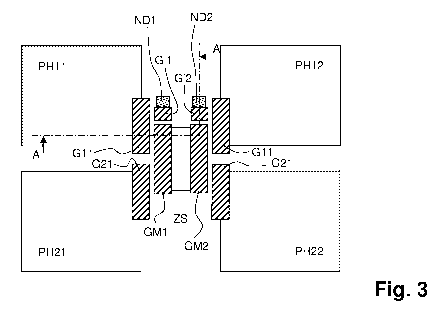
Figure 3 shows a top view of an organisational schematic of a
group of four columnwise- and rowwise-adjacent pixels, allowing, according
to the invention, the pixels to be read in a simple read mode of each pixel or
in a grouped read mode of four pixels, for an improved sensitivity, without a
digital summation operation being required. The photodiodes, the transfer
gates, the charge storage nodes, etc., are represented by simple rectangles
in order to simplify the figure, but their geometrical shapes may be more
complex in order to best fill the available space without increasing the pitch
of
the pixels or decreasing the optical aperture of the pixels. The electrical
connections shown in the diagram in figure 2 are not shown.
A multiplication structure common to the four adjacent pixels is
placed in a free space located between the four pixels. This structure makes
it possible to perform an electron multiplication in the case where a grouped-
mode readout of the electrons accumulated by the four pixels is carried out.
Each of the four pixels comprises a respective photodiode, PH11
and PH12 for the two pixels of a first row and PH21 and PH22 for the pixels
of the second row. The pixels PH11 and PH21 belong to a first column and
the pixels PH12, PH22 belong to the second column.
A primary transfer gate G11 (playing the role of the transistor Ti in
figure 2) is adjacent on one side to the photodiode PH11 and on the other to
a first multiplication gate GM1 of the multiplication structure associated
with
the group of four pixels. The primary transfer gate G11 allows charge to be
transferred from the first photodiode PH11 to the multiplication structure;
this
charge arrives via the first multiplication gate.
A second primary transfer gate G21 is adjacent on one side to the
photodiode PH21 and on the other to the same first multiplication gate GM1.
It allows charge to be transferred from the photodiode PH21 to the first
multiplication gate.
Symmetrically, for the two photodiodes of the second column, two
other primary transfer gates G12 and G22 are adjacent on one side to these
two photodiodes, PH21 and PH22 respectively, and on the other side to a
CA 02927430 2016-04-14
8
second multiplication gate GM2 of the multiplication structure. They allow
charges to be transferred from these two other photodiodes to the second
multiplication gate.
The multiplication structure may comprise, in its preferred version,
two gates GM1 and GM2 and potential switching means for alternately
passing one of the gates to a high potential while the other gate is at a low
potential and vice versa. The electron multiplication coefficient obtained
with
this structure depends on the potentials applied and on the number of
alternations applied.
Preferably, the multiplication gates are separated by an
intermediate semiconductor zone ZS kept at a constant potential
intermediate between the high and low potentials applied to the gates. During
a multiplication operation, packets of electrons, which transit alternately
from
the first multiplication gate to the second, and vice versa, pass through this
intermediate zone. This mechanism for multiplying electrons under the effect
of alternations of potentials applied to the multiplication gates on either
side
of the intermediate zone ZS is illustrated in detail in the aforementioned
European patent application EP 2 503 596, notably with regard to its figure 4.
The four-pixel structure according to the invention contains two
other charge reading structures, one associated with the first multiplication
gate GM1 and the other with the second multiplication gate GM2,
respectively. These read structures serve to read the charge stored under the
first multiplication gate and the charge stored under the second
multiplication
gate, respectively.
The first read structure comprises a charge storage node ND1, a
secondary transfer gate G'1 adjacent both to the first multiplication gate and
to the storage node ND1. This secondary transfer gate allows the electrons
present under the first multiplication gate, which may or may flot have
undergone a multiplication step, to be transferred to the storage node. The
first read structure furthermore comprises the following elements: a
transistor
(flot shown) for resetting the potential of the storage node ND1 and formed in
the same way as the transistor T2 of a conventional active pixel; a read
transistor in voltage-follower connection formed in the same way as the read
transistor T4 of a conventional active pixel; and a row selection transistor
CA 02927430 2016-04-14
9
formed and connected in the same way as the selection transistor T5 of a
conventional active pixel. Ail these elements form part of the first read
structure, which is associated with the two pixels of the first column, i.e.
with
the photodiodes PH11 and PH21.
The second read structure is associated with the two other pixels
belonging to the second column, therefore with the photodiodes PH12 and
PH22. It is identical to the first structure and functions in the same way. It
comprises a charge storage node ND2, a secondary transfer gate G'2
adjacent to the second multiplication gate GM2 and to the storage node ND2.
It also comprises, in the same way as the first structure, the following
elements (not shown): a transistor for resetting the second storage node, a
follower read transistor and a row selection transistor.
The row selection transistors of the two structures are controlled
simultaneously by the same row conductor.
The structure may function in a simple read mode or a grouped
read mode.
In the simple read mode, an electronic rolling shutter (ERS) mode
is used, i.e. the charge integration time is identical for the various rows
but
offset in time from one row to the following; the photodiodes integrate charge
from the end of the preceding integration cycle, the integration period
starting
at the end of a transfer of charge out of the photodiode and terminating for
each row at the end of a new transfer of charge out of the photodiode; the
instants of transfer are offset from one row to the following;
a) during this integration, the potential of the storage nodes
of the selected row is reset, for example the nodes ND1, ND2 of the
first row (photodiodes PH11 and PH12);
b) the reset level of these nodes is read;
c) at the end of the integration time, the charges of the
pixels of the first row (photodiodes PH11 and PH12) are transferred,
by way of the primary transfer gates G11 and G12, to under the
multiplication gates GM1 and GM2, respectively; for this purpose, the
multiplication gates GM1 and GM2 are raised to a sufficiently high
potential relative to the intrinsic potential of the photodiode;
CA 02927430 2016-04-14
d) the charge stored under the multiplication gate GM1 is
transferred ta the storage node ND1, by way of the secondary transfer
gate G'1, and, simultaneously or in succession, the charge stored
under the multiplication gate GM2 is transferred ta the storage node
5 ND2, by way of the secondary transfer gate G'2; the intrinsic potential
of the zone ZS forms a potential barrier in order to prevent the charges
present under the gates GM1 and GM2 from mixing;
e) the potential of the storage nodes ND1 and ND2,
representing the amount of light received by the photodiodes PH11
10 and PH12, respectively, is read; and
f) the operations a) ta e) are repeated for the following row
comprising the photodiodes PH21 and PH22, by opening the primary
transfer gates G21 and G22 in step c) and using the same
multiplication gates, the same secondary transfer gates Cl and G'2
and the same storage nodes ND1 and ND2 as above;
then the same operations are carried out for the pairs of rows of
following rank.
Alternatively, a half-frame readout could be carried out by first
reading ail the rows of photodiodes of uneven rank then ail the rows of even
rank.
In this simple read mode, the multiplication gates were used as
simple intermediate storage gates between the photodiodes and storage
nodes.
ln a grouped read mode, the charges of the four photodiodes
PH11, PH12, PH21, PH22 are gathered in the multiplication structure, these
charges are multiplied, stored under one of the two multiplication gates and
read by the read structure associated with this multiplication gate, for
example the read structure comprising G'1 and ND1 if it is a question of the
first multiplication gate GM1.
The read procedure then proceeds as follows: the four
photodiodes integrate charges, preferably in a global shutter mode in which
the instant at which charge integration starts and the instant at which charge
integration ends is the same for ail the photodiodes; this time is optionally
CA 02927430 2016-04-14
11
adjustable if there is a transistor (such as T3 in figure 2) for resetting the
potential of each photodiode, this transistor being controlled simultaneously
for ail the photodiodes;
a) during this integration, the potential of the storage nodes
ND1 and ND2 is reset; at the same time, the other groups of four
pixels are reset;
b) at the end of the integration period, charge is transferred
from the photodiodes via the primary transfer gates G11, G12, G21,
G22; the charges of the photodiodes of the first column (PH11 and
PH21) are transferred to under the multiplication gate GM1; the
charges of the two other photodiodes (PH12 and PH22) are
transferred at the same time or immediately afterwards to under the
multiplication gate GM2;
c) an electron multiplication is optionally performed by
applying an alternation of potentials in phase opposition to the
multiplication gates GM1 and GM2; the multiplication or absence of
multiplication is terminated by storing the multiplied charges under one
of the two multiplication gates, for example the gate GM1; the phase
opposition is non-overlapping insofar as the two gates must not
simultaneously be at the low potential; it may be preferable, for this
purpose, for the high levels of the potentials to overlap slightly; and
d) for a pair of rows, using the read structure associated
with this pair, the reset level of the storage node ND1 or ND2 (i.e. that
to which the charge is transferred) is read; then the charge stored
under the multiplication gate (here Cl) is transferred to the
corresponding storage node (ND1), and the level of the potential of
this node is read; the procedure is restarted for the other pairs of rows.
Therefore, in this mode the sum of the charges of four
photodiodes is read, these charges being mixed and multiplied in the
multiplication structure (GM1, ZS, GM2).
In the grouped read mode it is possible to benefit both from global
shutter operation and a correlated double sampling readout in which the
storage node is reset and read before charge is transferred to this storage
CA 02927430 2016-04-14
12
node and read. In the simple read mode it is necessary to use an ERS
(rolling shutter) operating mode.
In the embodiment in figure 3, there is one row of multiplication
structures and of read structures for two rows of photodiodes. In a variant
embodiment shown in figure 4, provision may be made for there to be as
many rows of multiplication structures as there are rows of photodiodes, but
there is, as shown in figure 3, only one multiplication structure common to
two pixels belonging to adjacent rows. Therefore, in this case each
photodiode has two primary transfer gates allowing charge to be transferred
to either one of two multiplication structures belonging to two adjacent rows.
However, this embodiment takes up more space than the embodiment in
figure 3. It will be noted that it is possible to operate the sensor in a
global
shutter mode by simultaneously actuating ail the transfer gates that have the
same position relative to the photodiodes. It is possible with the embodiment
in figure 4 to carry out a simple read operation without multiplication, or a
grouped read operation of four pixels with or without multiplication.
As a variant of figures 3 and 4, provision could be made, as is for
example shown in figure 5, for there to be one multiplication structure on
each side of the photodiode. There is therefore then, in one row of
multiplication structures, as many multiplication structures as there are
columns of photodiodes. If this arrangement is combined with that in figure 4,
the arrangement in figure 5 is obtained, there being, in this arrangement,
four
primary transfer gates for each photodiode, these gates allowing charge to
be transferred to one of four multiplication structures belonging to two
adjacent rows and two adjacent columns, respectively.
This makes it possible, in the grouped read mode, to choose the
adjacent pixels to be grouped. This embodiment is also less compact than
that in figure 3.
Figure 6 shows a technological cross section of the pixel, showing
one practical way of producing the sensor according to the invention. Figure
6 is a lateral cross section along the line A-A in figure 3. This line A-A
passes
through the photodiode PH11, the primary transfer gate G11, the
CA 02927430 2016-04-14
13
multiplication gate GM1, the pinned intermediate semiconductor zone ZS, the
secondary transfer gate G'2, and the storage node ND2. Figure 6 also shows
elements that are flot shown in figure 3, namely a transistor for resetting
the
storage node ND2, i.e. the transistor T2 in figure 2; lastly, the electrical
connection, according to the schematic diagram in figure 2, between the
storage node ND2 and two transistors T4 and T5 (follower transistor and row
selection transistor connected to a column conductor COL) has been
recalled. The transistor for resetting the photodiode PH11 (transistor T3 in
figure 2) is flot shown; it comprises a control gate allowing the charge of
the
photodiode to be transferred to a drain (flot shown) at the start of an
integration period.
The pixel is formed on a substrate 10 that preferably comprises a
weakly p-doped or p-doped (the p- symbol is used to designate this weak
doping) semiconductor active layer 12 formed on the surface of a more
strongly doped (p+) layer. The pixel is isolated from the neighbouring pixels
by an isolating barrier 13 that completely encircles it. This barrier may be a
shallow trench isolation above a p-type well.
The pixel comprises the photodiode region PH11 the perimeter of
which follows the outline of an n-type semiconductor region 14 implanted in a
portion of the depth of the active layer 12. This implanted region is
surmounted by a p+-type surface region 16 that is kept at a zero reference
potential. lt is a question of a pinned photodiode (i.e. the potential of the
p+-
type surface region is fixed). The zero reference potential is that applied to
the p--type active layer. In the simplest case, it is the potential of the p+-
type
substrate located under the active layer and applying its own potential to the
active layer; the surface region 16 is for example kept at this zero potential
because the region 16 touches a deep p+-type diffusion region 15 that makes
contact with the substrate 10. Electrical contact can also be made to this
diffusion region 15 in order to apply, via this contact, a zero potential to
the
region 16.
The charge storage node ND2 is an n-type diffusion region in the
active layer 12. A contact is formed on the storage node, in order to allow
the
potential of this region to be applied to the gate of a follower transistor
(T4),
in order to transform the amount of charge held by the storage node into an
electrical voltage level.
CA 02927430 2016-04-14
14
The gate of the transistor T2 allows charge to be emptied from the
storage node into an evacuation drain 20 that is an -type region connected
to a positive reset potential Vref.
The multiplication structure MS comprises the insulated gates
GM1 and GM2 separated by the semiconductor zone ZS. This zone is
formed, in the same way as the photodiode (but not necessarily with the
same doping density) by an n-type region 34 diffused into the active layer 12,
this region being covered by a p -type surface region 36. This region 36 is
for
example kept at the zero reference potential because it touches (not shown
in figure 6) a deep p+-type region that makes contact with the substrate,
analogously to the region 15 that touches the region 16 of the photodiode.
The region ZS is at an internai built-in potential fixed by keeping the region
36 at the reference potential of the active layer 12, here that of the
substrate
10.
The primary transfer gate G11 is a gate insulated from the active
layer 12; it is located between the photodiode Pl-111 and the multiplication
gate GM1 and it allows charge to be transferred from the photodiode to the
gate GM1.
The secondary transfer gate G'2 is an insulated gate located
between the multiplication gate GM2 and the storage node ND2.
The multiplication gates GM1 and GM2 are also gates that are
insulated from the active layer. They are separated from the gate G11 and
gate G'2, respectively, by a narrow interval (as narrow as possible given the
technology used) in which the semiconductor may not have a specific doping,
i.e. it may be directly made up of the active layer 12.
Potential switching means are provided for applying directly to the
multiplication gates GM1 and GM2 high potentials (higher than zero) or low
potentials (lower than zero) depending on the transfer or amplification phase
in question. These switching means are not shown because they are not
located in the pixel.
To transfer charges from the photodiode to the multiplication gate
GM1, the potential present under this gate and under the primary transfer
gate G11 is lowered by increasing their potential. The pinned zone ZS forms
a potential barrier that prevents the passage of these charges to the gate
GM2.
CA 02927430 2016-04-14
For the charge multiplication, a multiplicity (several tens, hundreds
or even thousands) of alterations of potentials in phase opposition are
applied to the gates GM1 and GM2 while leaving the zone ZS at a potential
intermediate between a high potential and a low potential of this alternation.
5 The charge stored under the gate GM1 is alternately switched from the gate
GM1 to the gate GM2 and vice versa. The electric fields seen by the
electrons are sufficiently high to accelerate the electrons and thus create
electron/hole pairs and therefore additional electrons in each alternation.
The
electron gain during one alternation is very low but it is multiplied by the
10 number of alternations. The potential of the primary and secondary transfer
gates is a low potential during the multiplication, creating a potential
barrier
preventing the charge from exiting the multiplication structure and confining
this charge alternately under the gate GM1 and under the gate GM2.
At the end of the multiplication, the charge remains stored under
15 the gate GM2 if the alternation is stopped when the gate GM2 has a high
potential; it could in the contrary case remain stored under the gate GM1. If
the charge remains under the gate GM2, the secondary transfer gate G'2 is
temporarily raised to a high potential allowing the charge to be passed to the
storage node ND2 with a view to reading this charge with the transistors T4
and T5 using a conventional read process.