Note: Descriptions are shown in the official language in which they were submitted.
CA 02928253 2016-04-21
WO 2015/062023
PCT/CN2013/086320
1
OPTICAL LENS AND LED LIGHT MODULE FOR BACKLIGHTING
BACKGROUND
[0001] Embodiments of thepresent disclosure relate generally to LED
lighting,
and more particularly to, backlighting LED systems for illuminating a target
surface
of a fixture such as a channel letter sign.
[0002] Channel letters are metal or plastic letters that are commonly
used on the
buildings of business and other organizations for exterior signage.At least
some of the
channel letters include a backlighting system which employs a plurality of
light
emitting diode (LED) devices for illuminating a frontface of the channel
letter, so that
the channel letter is viewable in a dark environment. Traditionally, to reduce
the
amount of LED devices used in the channel letters at least for cost and energy
saving
reasons, multiple optical lenses are used to distribute the light beams
emitted from the
plurality of LED devices in a manner to allow the light beams to be uniformly
distributed on the front face even though the LED devices may not be evenly
spaced
apart from each other behind the front face of the sign.
[0003] One exemplary design of the optical lens that has been proposed
for use
with the channel letter is described in US patent application publication US
2013/0042510A1, entitled "LED Lighting Module for Backlighting," by Nall et
al.
As described in this patent application, the lens has a rotated symmetrical
profile or
has a spherical outer surface which evenly distributes light beams emitted
from the
LED devices. One limitation in association with the use of the rotated
symmetrical
profile lens is that the LED light module constructed with the lens and the
LEDs may
not be able to be fit into a channel letter having a shallow depth and/or a
narrow width.
Another limitation in association with the use of the rotated symmetrical
profile lens
within a narrow channel letter is that the efficiency of the LED light module
is low
due to the amount of light that needs to reflect from the narrow side walls.
CA 02928253 2016-04-21
WO 2015/062023
PCT/CN2013/086320
2
[0004] Therefore, it is desirable to providean improved optical lens
and an LED
light module incorporating the improved lens to address at least one of the
limitations
of the prior lens design.
BRIEF DESCRIPTION
[0005] In accordance with one aspect of the present disclosure,an LED light
module for illuminating a target plane is provided. The LED light module
includes a
first LED source, a second LED source disposed adjacent the first LED source,
a first
lens covering the first LED source, and a second lens covering the second LED
source.
The first lens is configured to direct first light beams emitted from the
first light
source to the target plane. The second lens is configured to direct second
light beams
emitted from the second light source to the target plane. At least one of the
first and
second lenses is shaped to have an asymmetrical profile.
[0006] In accordance with another aspect of the present disclosure, a
backlighting system is provided. The backlighting system includes a plurality
of LED
light modules electrically coupled with one another. One of the plurality of
LED light
modules includes a circuit board, a first LED source mounted on the circuit
board, a
second LED source mounted on the circuit board, andan optical element mounted
on
the circuit board and covering both the first LED source and the second LED
source.
The optical element is configured to distribute the light beams emitted from
at least
one of the first and second LED sources into asymmetrical light patterns.
[0007] In accordance with another aspect of the present disclosure,a
fixture for
presenting a visible sign to a viewer is provided. The fixture includes a
target plane
anda backlighting system for directing light beams to the target plane. The
backlighting system includes a plurality of LED light modules electrically
coupled
with one another. One of the plurality of LED light modules includes a circuit
board,
a first LED source mounted on the circuit board, a second LED source mounted
on
the circuit board, andan optical element mounted on the circuit board and
covering
both the first LED source and the second LED source. The optical element is
configured to distribute the light beams emitted from at least one of the
first and
CA 02928253 2016-04-21
WO 2015/062023
PCT/CN2013/086320
3
second LED sources into a first light pattern and a second light pattern
different than
the first light pattern.
DRAWINGS
[0008] These and other features, aspects, and advantages of the
present
disclosure will become better understood when the following detailed
description is
read with reference to the accompanying drawings in which like characters
represent
like parts throughout the drawings, wherein:
[0009] FIG. 1 is aperspective view of a backlightingsystem in
accordance with
an exemplary embodiment of the present disclosure;
[0010] FIG. 2 is across-sectional view of an LED light module of the
backlighting system shown in FIG. 1 taken along line 1-lin accordance with one
exemplary embodiment of the present disclosure;
[0011] FIG. 3 is a perspective view of an optical element used in the
LED light
module shown in FIG. 2 in accordance with another exemplary embodiment of the
present disclosure;
[0012] FIG. 4 is a cross-sectional view of the optical element shown
in FIG. 3
taken along line 2-2in accordance with an exemplary embodiment of the present
disclosure;
[0013] FIG. 5 is a polar plot illustrating a light distribution
pattern of light
beams emitted from one LED light module in accordance with an exemplary
embodiment of the present disclosure;
[0014] FIG. 6 is anilluminance distribution of light beams emitted
from one
LED light module in accordance with an exemplary embodiment of the present
disclosure; and
CA 02928253 2016-04-21
WO 2015/062023
PCT/CN2013/086320
4
[0015] FIG. 7 is anilluminance distribution of light beams provided
from a
plurality of LED light modules in accordance with an exemplary embodiment of
the
present disclosure.
DETAILED DESCRIPTION
[0016] Embodiments of the present disclosure are directed to an improved
optical element used in a backlighting system or an LED light module. More
specifically, an optical element configured with an asymmetrical optical
profile is
proposed for distributing light pattern asymmetrically in a target plane. One
technical
benefit or advantage in association with the use of the asymmetrical optical
element is
that the LED light module constructed with the proposed optical element can be
fit
into a fixture such as a channel letter can with a shallow depth and/or a
narrow width.
Another technical benefit or advantage in association with the use of the
asymmetrical
optical element is that the overall efficiency is improved. Yet another
technical
advantage or benefit in association with the use of the asymmetrical optical
element is
the LED count for LEDs located between two parallel sidewalls in a display
lighting
device or an enclosure can be minimized. The sidewalls could be reflective,
translucent, and/or transparent. For example, the LED light module could be
used
between two pieces of glass or plastic to create lighting effects within
fixtures or
displays by spreading light uniformly down the channel between the faces.
Other
technical advantages or benefits will become apparent to those skilled in the
art by
referring to the detailed descriptions and accompanying drawings provided
below in
accordance with one or more embodiments of the present disclosure.
[0017] In an effort to provide a concise description of these
embodiments, not
all features of an actual implementation are described in the one or more
specific
embodiments. It should be appreciated that in the development of any such
actual
implementation, as in any engineering or design project, numerous
implementation-
specific decisions must be made to achieve the developers' specific goals,
such as
compliance with system-related and business-related constraints, which may
vary
from one implementation to another. Moreover, it should be appreciated that
such a
development effort might be complex and time consuming, but would nevertheless
be
CA 02928253 2016-04-21
WO 2015/062023
PCT/CN2013/086320
a routine undertaking of design, fabrication, and manufacture for those of
ordinary
skill having the benefit of this disclosure.
[0018] Unless defined otherwise, technical and scientific terms used
herein have
the same meaning as is commonly understood by one of ordinary skill in the art
to
5 which this disclosure belongs. The terms "first," "second," and the like,
as used
herein do not denote any order, quantity, or importance, but rather are used
to
distinguish one element from another. Also, the terms "a" and "an" do not
denote a
limitation of quantity, but rather denote the presence of at least one of the
referenced
items. The term "or" is meant to be inclusive and mean either any, several, or
all of
the listed items. The use of "including," "comprising" or "having" and
variations
thereof herein are meant to encompass the items listed thereafter and
equivalents
thereof as well as additional items. The terms "connected" and "coupled" are
not
restricted to physical or mechanical connections or couplings, and can include
electrical connections or couplings, whether direct or indirect.
[0019] As used in the present disclosure, the term "LED" should be
understood
to include any electroluminescent diode or other type of carrier
injection/junction-
based system that is capable of generating radiation in response to an
electric signal.
Thus, the term LED includes, but is not limited to, various semiconductor-
based
structures that emit light in response to current, light emitting polymers,
electroluminescent strips, and the like.
[0020] In particular, the term LED refers to light emitting diodes of
all types
(including semi-conductor and organic light emitting diodes) that may be
configured
to generate radiation in one or more of the infrared spectrum, ultraviolet
spectrum,
and various portions of the visible spectrum. Some examples of LEDs include,
but are
not limited to, various types of infrared LEDs, ultraviolet LEDs, red LEDs,
blue LEDs,
green LEDs, yellow LEDs, amber LEDs, orange LEDs, and white LEDs. It also
should be appreciated that LEDs may be configured to generate radiation having
various bandwidths for a given spectrum (e.g., narrow bandwidth, broad
bandwidth).
CA 02928253 2016-04-21
WO 2015/062023
PCT/CN2013/086320
6
[0021] For example, one implementation of an LED configured to
generate
essentially white light (e.g., a white LED) may include a number of dies which
respectively emit different spectra of electroluminescence that, in
combination, mix to
form essentially white light. In another implementation, a white light LED may
be
associated with a phosphor material that converts electroluminescence having a
first
spectrum to a different second spectrum. In one example of this
implementation,
electroluminescence having a relatively short wavelength and narrow bandwidth
spectrum "pumps" the phosphor material, which in turn radiates longer
wavelength
radiation having a somewhat broader spectrum.
[0022] It should also be understood that the term LED does not limit the
physical and/or electrical package type of an LED. For example, as discussed
above,
an LED may refer to a single light emitting device having multiple dies that
are
configured to respectively emit different spectra of radiation (e.g., that may
or may
not be individually controllable). Also, an LED may be associated with a
phosphor
that is considered as an integral part of the LED (e.g., some types of white
LEDs). In
general, the term LED may refer to packaged LEDs, non-packaged LEDs, surface
mount LEDs, chip-on-board LEDs, T-package mount LEDs, radial package LEDs,
power package LEDs, LEDs including some type of encasement and/or optical
element (e.g., a diffusing lens), etc.
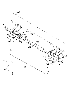
[0023] Referring to FIG. 1, a perspective view of a backlighting system 100
in
accordance with an exemplary embodiment of the present disclosure is
illustrated.
The backlighting system 100 can be used in a fixture such as a channel letter
or any
other appropriate display lighting devices and enclosures. As shown in FIG. 1,
the
back lighting system 100 includes a first LED light module 110 and a second
LED
light module 130. The first LED light module 110 and the second LED light
module
130 may be disposed at an inner space defined by the channel letter can. The
first
LED light module 110 and the second LED light module 130 are configured to
illuminate at least one surface such as a top surface of the channel letter to
present a
visible sign to a viewer in a dark environment. In one embodiment, the first
LED
light module 110 and the second LED light module 130 are electrically
connected
with one another in a serialmanner via two electrical conductors 102, 104,
such as
CA 02928253 2016-04-21
WO 2015/062023
PCT/CN2013/086320
7
electrical wires. In some embodiments, the two electrical conductors 102, 104
may be
arranged to be flexible or retractable, such that a distance between the first
LED light
module 110 and the second LED light module 130 can be adjusted according to
practical requirements. Although two LED light modules are illustrated, in
other
embodiments, it is contemplated that fewer or more LED light modules may be
used
in the backlighting system 100 for a particular application. In some
embodiments,
additionally or alternatively, two or more LED light modules may be
electrically
connected in parallel manner.
[0024] In some embodiments, the first LED light module 110 and the
second
LED light module 130 may be mounted to a channel letter can in any appropriate
means. For example, as shown in FIG. 1, a double-side tape 116 attached to the
bottom surface of a housing 118 of the first LED light module 110 can be used
to fix
the first LED light module 110 to an inner surface (e.g., back surface or
bottom
surface) of a channel letter can (not shown). In other embodiments, the first
LED
light module 110 may be fixed to the inner surface of the channel letter can
using
screws or any other appropriate fasteners. In a similar manner, as shown in
FIG. 1,
another double-side tape 136 attached to the bottom surface of a housing 138
of the
second LED light module 130 can be used to fix the second LED light module 130
to
an inner surface (e.g., back surface or bottom surface) of the channel letter
can. In
other embodiments, the second LED light module 110 may be fixed to the inner
surface of the channel letter sign using screws or any other appropriate
fasteners.
[0025] When energized, the first LED light module 110 is operated to
direct
first light beams (generally designated as 112) emitted from a plurality of
first LED
light sources (not shown in FIG. 1, will be described in detail with reference
to FIG. 2)
disposed at the inside of housing 118 of the LED light module 110 at a target
plane
140 such as a front face or top surface of a channel letter sign. In the
illustrated
embodiment, the first LED light module 110 includes an optical element 120
which
extends through an opening 122 defined at a top surface of the housing 118 of
the first
LED light module 110. The optical element 120 is configured to direct light
beams
emitted from the first LED light sources to the target plane 140 to make the
channel
letter viewable. In some embodiments, the optical element 120 is configured
with
CA 02928253 2016-04-21
WO 2015/062023
PCT/CN2013/086320
8
refractive surfaces to diverge the light beams emitted from the light sources,
such that
the target plane can be illuminated with light beams having good optical
uniformity.
In one embodiment, the optical element 120 is an integrally formed optimal
element
which includes a first lens 124, a second lens 126, and a third lens 128 that
are closely
connected with one another. In other embodiments, the optical element 120 may
include separately manufactured lenses which may be spaced apart from one
another.
[0026] In the illustrated embodiment of FIG. 1, each of the first lens
124, the
second lens 126, and the third lens 128 is arranged to have substantially the
same
optical profile. For example, each of thefirst lens 124, the second lens 126,
and the
third lens 128 may be arranged to have an asymmetrical optical profile, such
that each
of the first lens 124, the second lens 126, and the third lens 128 can
distribute the light
beams emitted from the first LED sources to the target plane 140
asymmetrically. As
used herein, "asymmetrical profile" and/or "asymmetrical optical profile"
refers to
that the optical element or the optical lens is arranged to have at least two
different
types of optical refractive surfaces for refracting the light beams provided
from the
LED light sources. For example, the optical element or the optical lens may
have one
or more curved outer surfaces for diverging the light beams provided from the
LED
light sources, and one or more flat surfaces for refracting the light beams
provided
from the LED light sources.
[0027] In a specific embodiment, as represented in a O-XYZ Cartesian
coordinate system, each of the first lens 124, the second lens 126, the third
lens
128can be configured in manner to allow the light beams 112 distributed in a
first
light pattern along the O-X direction having a larger light intensity than
that of the
light beams 112 distributed in a second light pattern along the O-Y direction
which is
substantially perpendicular to the O-X direction. As such, asymmetrical light
patterns
of the light beams emitted from the LED light sources can be achieved. In
other
embodiments, it is contemplated that not all the three lens 124, 126, 128 are
configured to have asymmetrical profiles. Instead, at least some of the lens
124, 126,
128 can be arranged to have symmetrical profiles. For example, in some
embodiments, the first lens 124 and the third lens 128 may be arranged to have
an
asymmetrical profile, and the second lens 126 is arranged to have a
symmetrical
CA 02928253 2016-04-21
WO 2015/062023
PCT/CN2013/086320
9
profile. One example of the symmetrical profile of the optical lens 126 is a
rotated
symmetrical profile such as a spherical surface.
[0028] In a similar manner, the second LED light module 130 is
operated to
direct second light beams (generally designated as 132) emitted from a
plurality of
second LED light sources (not shown in FIG. 1) at the target plane 140 of the
channel
letter sign. In some embodiments, a pitch between the first LED light module
110 and
the second LED light module 130 can be adjusted to allow the second light
beams 132
emitted from the second LED light module 130 to be overlapped with the first
light
beams 112 emitted from the first LED light module 110 to ensure uniform light
distribution on the target plane 140.
[0029] In the illustrated embodiment, the second LED light module 130
includes an optical element 150 which extends through an opening 142 defined
at a
top surface of the housing 138 of the second LED light module 130. The optical
element 150 is configured for directing light beams emitted from the second
LED
light sources to the target plane 140. In one embodiment, the optical element
150 is
an integrally formed optimal element which includes a first lens 144, a second
lens
146, and a third lens 148 that are connected closely with one another. In
other
embodiments, the optical element 150 may include separately manufactured
lenses
which may be spaced apart from one another.
[0030] In the illustrated embodiment of FIG. 1, each of the first lens 144,
the
second lens 146, and the third lens 148 of the second LED light module 130 is
arranged to have substantially the same optical profile. For example, each of
thefirst
lens 144, the second lens 146, and the third lens 148 may be arranged to have
an
asymmetrical optical profile, such that each of the first lens 144, the second
lens 146,
and the third lens 148 can distribute the light beams emitted from the second
LED
sources to the target plane 140 asymmetrically.
[0031] In a specific embodiment, as represented in a O-XYZ Cartesian
coordinate system, each of the first lens 144, the second lens 146, the third
lens 148
can be configured in manner to allow the light beams 132 distributed in a
first light
CA 02928253 2016-04-21
WO 2015/062023
PCT/CN2013/086320
pattern along the O-X direction having a larger light intensity than that of
the light
beams 132 distributed in a second light pattern along the O-Y direction which
is
substantially perpendicular to the O-X direction. As such, asymmetrical light
patterns
of the light beams emitted from the second LED light sources can be achieved.
In
5 other
embodiments, it is contemplated that not all the three lenses 144, 146, 148
are
configured to have asymmetrical profiles. Instead, at least some of the lens
144, 146,
148 can be arranged to have symmetrical profiles. For example, in some
embodiments, the first lens 144 and the third lens 148 may be arranged to have
an
asymmetrical profile, and the second lens 146 is arranged to have a
symmetrical
10 profile.
One example of the symmetrical profile of the optical lens 146 is a rotated
symmetrical profile such as a spherical surface.
[0032]
Referring to FIG. 2, a cross-sectional view of an LED light module 200
is shown in accordance with an exemplary embodiment of the present disclosure.
The
LED light module 200 can be used as the first LED light module 110 and/or the
second LED light module 130 shown in FIG. 1 for directing light beams to
illuminate
the target plane 140 (see FIG. 1).
[0033] As
shown in FIG. 2, the LED light module 200 includes a main body or
housing 204 which may be made from over-molded plastic and used to accommodate
various elements ofthe LED light module 200. In one embodiment, the main body
204 may include a channel to allow a conductor 202 such as an electrical wire
to enter
from one side into the main body 204 and exit from an opposing side of the
main
body 204. The main body 204 may also include a mounting member 252 integrally
or
separately connected to the main body 204. In one embodiment, the mounting
member 252 is formed with an opening or through ho1e254 formounting or fixing
the
LED light module 200 to a channel letter can. As described earlier, the LED
light
module 200 may additionally or alternatively include a double-side tape 208
attached
to a bottom surface of the main body 204. In one embodiment, the double-side
tape
208 can be attached to a back surface of the channel letter can to fix the LED
light
module 200 in position with the channel letter can.
CA 02928253 2016-04-21
WO 2015/062023
PCT/CN2013/086320
11
[0034] In
one embodiment, the LED light module 200 includes a circuit board
206 such as a printed circuit board which is disposed inside of the main body
204.
The circuit board 206 is electrically coupled to the conductor 202 for
receiving
electrical current supplied through the conductor 202. In one embodiment, the
circuit
board 206 includes a first surface 222 and a second surface 224. In one
embodiment,
the first surface 222 is configured to mount a plurality of LED sources 232,
234, 236.
The second surface 222 is configured to mount various other elements, such as
a LED
controller 242, one or more resistors 244, and one or more diodes 246 which
are in
electrical connection with at least one of the LED sources 232, 234, 236 to
ensure the
LED sources 232, 234, 236 to function properly.
[0035] In
one embodiment, the plurality of LED sources 232, 234, 236 are
mechanically and electrically coupled to the circuit board 206 by solder for
example.
Although three LED sources 232, 234, 236 are depicted in FIG. 2, in other
embodiments, the LED light module 200 may include fewer or more LED sources.
In
some embodiments, the three LED sources 232, 234, 236 are arrayed along a
straight
line. In other embodiments, the three LED sources 232, 234, 236 may be arrayed
along a non-straight line, such as in a circle, semi-circle, an ellipse, and
any other
appropriate geometry shapes. Also, in the illustrated embodiment, the three
LED
sources 232, 234, 236 are spaced apart from one another at a predetermined
distance.
The predetermined distance can be varied according to a number of factors such
as the
type of the LED sources being used and optical lens used in association with
the LED
sources.
[0036] With
continued reference to FIG. 2, the first surface 222 of the circuit
board 206 is further configured to mount one or more optical elements 210
thereon.
Further referring to FIG. 3, the optical element 210 is an integrally formed
optical
element which includes a first lens 212, a second lens 214, and a third lens
216. In the
illustrated embodiment, the first lens 212, the second lens 214, and the third
216 are
closely connected with each other without any interconnecting portions. That
is, each
of the three lenses 212, 214, 216 is physically contacting an adjacent one. In
other
embodiments, the three lenses 212, 214, 216 may be spaced apart with a
distance
CA 02928253 2016-04-21
WO 2015/062023
PCT/CN2013/086320
12
formed therebetween. Still in some embodiments, the three lenses 212, 214, 216
may
be separately manufactured and separately mounted to the circuit board 206.
[0037] In
the illustrated embodiment, the first lens 212, the second lens 214, and
the third lens 216 are also integrally formed with a supporting member 218
which is
used for supporting the three lenses 212, 214, 216 thereon. In addition, in
one
embodiment, the supporting member 218 includes two posts 266, 268 disposed at
two
corners of the supporting member 218. The two posts 266, 268 extending from
one
surface of the supporting member 218 are used to be fit into corresponding
recesses
and/or holes defined in the circuit board 206 to ensure the optical member 210
as well
as the three lenses 212, 214, 216 to remain in their proper positions. In
other
embodiments, the post-hole (or post-recess) mechanical configuration shown in
FIG.
3 for mounting together the optical element 210 and the circuit board 206 can
be
reversed. That is, the supporting member 210 may be formed with recesses
and/or
holes and the circuit board 206 is formed with corresponding posts for fitting
into the
recesses and/or holes. It is contemplated that this specific configuration
should not be
construed as limiting, and the optical element 210 can be mounted to the
circuit board
206 using any other appropriate means such as screws and/or adhesives.
[0038]
Further referring to FIGS. 2 and 3, each of the three lenses 212, 214, 216
defines a hollow chamber for covering and sealing the corresponding LED
sources
232, 234, 236. Sealing the LED sources 232, 234, 236 inside the corresponding
lenses 212, 214, 216 can prevent dust particles from falling onto these LED
sources
232, 234, 236 and also provide moisture resistant and waterproof conditions
for these
LED sources 232, 234, 236. In some embodiments, the three lenses 212, 214, 216
are
made from acrylic and/or polycarbonate material which is also transparent for
passing
through light beams emitted from the LED sources 232, 234, 236.
[0039] With
continued reference to FIGS. 2 and 3 and further referring to FIG. 4,
in one embodiment, the three lenses 212, 214, 216 are arranged to have the
same
profiles. In a specific embodiment, each of the three lenses 212, 214, 216 is
arranged
to have an asymmetrical profile to distribute light beams emitted from the
light
sources 232, 234, 236 in an asymmetrical manner. As shown in FIG. 3, the first
lens
CA 02928253 2016-04-21
WO 2015/062023
PCT/CN2013/086320
13
212 includes a first outer surface 262 which is a curved surface such as a
compound
curve surface, or more specifically an ellipsoidal surface. In one embodiment,
the
first outer surface 262 is arranged to have a uniform width measured along the
O-Y
direction. In other embodiments, the first outer surface 262 may be arranged
to have
other shapes such as a spherical-shaped surface and a non-spherical-shaped
surface.
[0040] As further shown in FIG. 4, the first lens 212 further includes
an inner
surface 265 which is also a curved surface such as a compound curve surface,
or more
specifically an ellipsoidal surface. The inner surface 265 cooperates with the
outer
surface 262 to define a wall having a varying thickness from the center of the
first
lens 212 to the edge of the first lens 212. The varying thickness wall
configuration
allows the light beams emitted from the first light source 232 to be diverged
at a wide
angle to a target plane. More specifically, the curved surface 265 configured
with a
uniform width allows significant portion of the light beams emitted from the
first light
source 232 to be distributed as a first light pattern along the O-X direction
of the
target plane 140.
[0041] Referring back to FIG. 3, the first lens 212 further includesa
second outer
surface 264 which is a planar surface in one embodiment. That is, the second
outer
surface 264 is connected perpendicularly to the first outer surface 262. In
addition,
the first lens 212 also includes a third outer surface (not viewable in FIG.
3) which is
arranged in parallel to the second outer surface 264 and connected
perpendicularly to
the first outer surface 262. As a result, the first outer surface 262, the
second outer
surface 264, and third outer surface constitutes the entire outer surface of
the first lens
212. The second outer surface 264 is configured to refract the light beams
emitted
from the first LED source 232 and distribute the light beams in the target
plane 140
(see FIG. 1) in a second light pattern. In one embodiment, the planar outer
surface
264 is configured to generate the second light pattern having a much smaller
intensity
than that of the first light pattern generated by the curved outer surface
262. As can
be understood, configuring the optical element 210 or the lenses 212, 214, 216
with
planar surfaces allows the optical element 210 or lenses 212, 214, 216 to be
fit into a
channel letter can having a narrower width measured along the O-Y direction.
In
CA 02928253 2016-04-21
WO 2015/062023
PCT/CN2013/086320
14
addition, less or even no light beams are distributed to the side surfaces of
the channel
letter sign, thus, the efficiency of the LED light module is improved.
[0042] As further shown in FIGS. 3 and 4, the second lens 214 and the
third lens
216 are configured to have the same optical profile as the first lens 212. For
example,
the second lens 214 includes a first curved outer surface 272, a second planar
outer
surface 274, a third planar outer surface (not visible in FIG. 3), and a
curvedinner
surface 267 for distributing light beams emitted from the second LED source
234
asymmetrically in the target plane140. The third lens 216 includes a first
curved outer
surface 282, a second planar outer surface 284, a third planar outer surface
(not visible
in FIG. 3), and a curved inner surface 269 for distributing light beams
emitted from
the third LED source 236 (see FIG. 2) asymmetrically in the target plane 140.
In
some embodiments, the light beams emitted from the three LED sources 232, 234,
236 and distributed by the three lenses 212, 214, 216 can be overlapped to
make a
more uniform light distribution on the target plane 140.
[0043] The optical lens 210 shown in FIGS. 2-4 can be modified in a variety
of
ways. For example, in one embodiment, in the case of covering three LED
sources
such as the LED sources 232, 234, 236, the optical lens 210 may be an
integrally
formed optical element configured to have two curved outer surfaces that are
connected without any intermediate portions. The optical lens 210 also has
planar
outer surfaces, such that the light beams emitted from the LED sources 232,
234, 236
can also be distributed asymmetrically in the target plane 140.
[0044] Referring to FIG. 5, which is a polar plot 310 illustrating
light
distribution of the light beams emitted from one LED light module 200 shown in
FIG.
2 in accordance with an exemplary embodiment of the present disclosure. As
shown
in FIG. 5, asymmetrical light patternsare provided by the LED light module
200. For
example, the first light pattern 312 shaped like a "batwing" represents the
light beams
distributed by the LED light module 200and measured along the O-X direction.
In
one embodiment, the first light pattern 312 along the O-X direction can
achieve a
wide viewing angle of about 140 degrees. The second light pattern 314
represents the
light beams distributed by the LED light module 200 and measured along the O-Y
CA 02928253 2016-04-21
WO 2015/062023
PCT/CN2013/086320
direction. The second light pattern 314 has smaller light intensities than the
first light
pattern 312. Therefore, the efficiency of the LED light module 200 can be
increased.
[0045]
Referring to FIG. 6, which illustrates different illuminance light patterns
of the light beams emitted from the LED light module 200 shown in FIG. 2 in
5
accordance with an exemplary embodiment of the present disclosure. As shown in
FIG. 6, a first illuminance light pattern 322 which has a substantially strip
shape
represents the light beams distributed from the LED light module 200 and
measured
along the O-X direction. A second illuminance light pattern 324 which also has
a
substantially strip shape perpendicular to the first illuminance light pattern
322
10
represents the light beams distributed from the LED light module 200 and
measured
along the O-Y direction. It can be seen that the second illuminance light
pattern 324
has a smaller illuminance value than that of the first illuminance light
pattern 322.
Therefore, the efficiency of the LED light module 200 can be increased.
[0046]
Referring to FIG. 7, which illustrates anilluminance distribution of the
15 light
beams generated by five LED light modules in accordance with an exemplary
embodiment of the present disclosure. The horizontal axis represents the
distance of a
position at the target plane relative to the center of the five LED light
modules. The
vertical axis represents the illuminance value measured at the target plane.
As
shownin FIG. 7, the light distribution of the improved LED light modules has a
light
uniformity of about 94% over a range of about 360 millimeters measured along
the 0-
X direction.
[0047]
While the invention has been described with reference to exemplary
embodiments, it will be understood by those skilled in the art that various
changes
may be made and equivalents may be substituted for elements thereof without
departing from the scope of the invention. Furthermore, the skilled artisan
will
recognize the interchangeability of various features from different
embodiments. In
addition, many modifications may be made to adapt a particular situation or
material
to the teachings of the invention without departing from the essential scope
thereof.
Therefore, it is intended that the invention not be limited to the particular
embodiment
disclosed as the best mode contemplated for carrying out this invention, but
that the
CA 02928253 2016-04-21
WO 2015/062023
PCT/CN2013/086320
16
invention will include all embodiments falling within the scope of the
appended
claims.