Note: Descriptions are shown in the official language in which they were submitted.
1
DESCRIPTION
DC POWER-SUPPLY DEVICE AND REFRIGERATION CYCLE DEVICE
Field
[0001] The present invention relates to a DC power-
supply device and a refrigeration cycle device that
includes the DC power-supply device.
Background
[0002] Conventional DC power-supply devices are known
that have an inverter as a load, with the invertor driving
a compressor motor used in an air conditioner, a heat-pump
water heater, a refrigerator, and a freezer, that are
connected to the load, and that convert an alternating
current into a direct current. Patent Literature 1, for
example, discloses a DC power-supply device that can
convert a single-phase alternating current into a direct
current and can boost the output voltage with a simple
configuration.
Citation List
Patent Literature
[0003] Patent Literature 1: Japanese Patent Application
Laid-open No. 2000-278955
Summary
[0004] However, according to the conventional technology
described above, if an excessive inrush current to a
capacitor is generated when a switching operation is
started, the inrush current cannot be suppressed.
Therefore, there is a problem in that elements in the
CA 2929041 2017-06-30
2
power-supply device may be broken and circuits in the
device may be burned out.
[0005] The present invention has been made in view of
the above problem, and an object of the present invention
is to provide a DC power-supply device that can suppress an
excessive inrush current generated when a switching
operation is started and can prevent breakage of elements
and burnout of circuits.
[0006] According to another aspect of the present
invention there is provided a DC power-supply device that
converts an alternating current from a three-phase AC power
supply into a direct current and supplies the converted
current to a load, the DC power-supply device comprising:
a rectifier circuit that has a reactor connected to an
input side or an output side thereof and that rectifies the
alternating current from the three-phase AC power supply;
a first capacitor and a second capacitor that are
connected in series between output terminals to the load;
a charging unit that selectively charges one or both
of the first capacitor and the second capacitor; and
a control unit that controls the charging unit,
wherein
the charging unit includes
a first switching element and a second switching
element that are connected in series and are switched
at a frequency that is a multiple n (n is a natural
number) of a frequency of the three-phase AC power
supply,
a first backflow prevention element that prevents
backflow of a stored electric charge of the first
capacitor to the first switching element, and
a second backflow prevention element that
CA 2929091 2017-06-30
2a
prevents backflow of a stored electric charge of the
second capacitor to the second switching element, and
a point between the first switching element and the
second switching element and a point between the first
capacitor and the second capacitor are connected to each
other,
the DC power-supply device further comprises a power-
supply voltage detection unit,
the control unit controls an operation mode,
the operation mode includes
a full-wave rectification mode in which the first
switching element and the second switching element are
always turned off and on-duty ratios of the first
switching element and the second switching element are
0%, and
a boosting mode in which the first switching
element and the second switching element are
alternately turned on at a charging frequency, and
in the boosting mode, an output voltage is controlled
by gradually increasing the on-duty ratios of the first
switching element and the second switching element.
According to another aspect of the present invention
there is provided a refrigeration cycle device comprising
the DC power-supply device as described herein.
CA 2929041 2017-06-30
3
[0007] According to the present invention, an effect may
be obtained where it is possible to obtain a DC power-
supply device that can suppress an excessive inrush current
generated when a switching operation is started and can
prevent breakage of elements and burnout of circuits.
Brief Description of Drawings
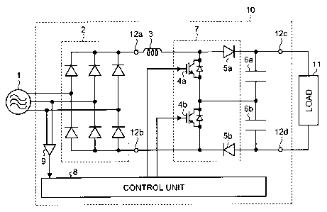
[0008] FIG. 1 is a diagram illustrating a configuration
example of a DC power-supply device according to a first
embodiment.
FIG. 2 is a diagram illustrating the correspondence
relation between switching control of a first switching
element and a second switching element and capacitors to be
charged, in the DC power-supply device according to the
first embodiment.
FIG. 3 is a diagram illustrating an operation mode of
the DC power-supply device according to the first
embodiment.
FIG. 4 is a diagram illustrating an example
representing switching patterns, a converter-output DC
voltage, and an example of simulation waveforms of
respective phase currents of a three-phase alternating
current in the DC power-supply device according to the
first embodiment.
FIG. 5 is a diagram illustrating a comparative example
representing switching patterns, a converter-output DC
voltage, and an example of simulation waveforms of
respective phase currents of a three-phase alternating
current in a conventional DC power-supply device.
FIG. 6 is a diagram illustrating switching signals
when the charging operation is started and during a normal
CA 2929041 2017-06-30
CA 02929041 2016-04-28
4
operation, where the signals are generated in a control
unit of the DC power-supply device according to the first
embodiment.
FIG. 7 is a diagram illustrating an example of a
switching-signal generation method executed by the control
unit of the DC power-supply device according to the first
embodiment.
FIG. 8 is a diagram illustrating an example of control
executed by a control unit of a DC power-supply device
according to a second embodiment.
FIG. 9 is a diagram illustrating a configuration
example of a DC power-supply device according to a third
embodiment.
FIG. 10 is a diagram illustrating a configuration
example of a refrigeration cycle device according to a
fourth embodiment.
Description of Embodiments
[0009] Exemplary embodiments of a DC power-supply device
and a refrigeration cycle device that includes the DC
power-supply device according to the present invention will
be explained below in detail with reference to the
accompanying drawings. The present invention is not
limited to the embodiments.
[0010] First embodiment.
FIG. 1 is a diagram illustrating a configuration
example of a DC power-supply device according to a first
embodiment of the present invention. A DC power-supply
device 10 illustrated in FIG. 1 converts a three-phase
alternating current supplied from a three-phase AC power
supply 1 into a direct current and supplies the converted
current to a load 11. The load 11 can be exemplified by an
inverter load that drives a compressor motor used in a
CA 02929041 2016-04-28
refrigeration cycle device.
[0011] The DC power-supply device 10 includes a
rectifier circuit 2 that rectifies a three-phase
alternating current; a reactor 3 connected to the output
5 side of the rectifier circuit 2; a first capacitor 6a and a
second capacitor 6b that are connected in series between
the output terminals to the load 11; a charging unit 7 that
selectively charges the first capacitor 6a and the second
capacitor 6b, a control unit 8 that controls the charging
unit 7; and a power-supply voltage detection unit 9 that
detects the voltage of a three-phase alternating current.
The power-supply voltage detection unit 9 detects the line
voltage between two phases (an r-phase and an s-phase) in a
three-phase alternating current supplied from the three-
phase AC power supply 1. For the convenience of
explanation, terminals 12a to 12d are illustrated in FIG. 1.
[0012] The rectifier circuit 2 is a three-phase full-
wave rectifier circuit in which six rectifier diodes are
connected in a full-bridge.
[0013] In FIG. 1, while the reactor 3 is a DC reactor,
it can be an AC reactor in which the reactor 3 is provided
on the input side of the rectifier circuit 2.
[0014] The charging unit 7 includes a first switching
element 4a, a second switching element 4b, a first backflow
prevention element 5a, and a second backflow prevention
element 5b.
[0015] The first switching element 4a controls charging
of the second capacitor 6b. The second switching element
4b controls charging of the first capacitor 6a. The first
switching element 4a and the second switching element 4b
can be exemplified by a power transistor, a power MOSFET
(Metal Oxide Semiconductor Field Emission Transistor), and
an IGBT (Insulated Gate Bipolar Transistor).
CA 02 9041 2016-048
6
[0016] The first backflow prevention element 5a is
connected in the forward direction from the collector of
the first switching element 4a toward the connection point
between the first capacitor 6a and the load 11, and
prevents backflow of an electric charge stored in the first
capacitor 6a to the first switching element 4a. The second
backflow prevention element 5b is connected in the forward
direction from the connection point between the second
capacitor 6b and the load 11 toward the emitter of the
second switching element 4b, and prevents backflow of an
electric charge stored in the second capacitor 6b to the
second switching element 4b.
[0017] The first capacitor 6a and the second capacitor
6b are set to have the same capacity, and the connection
point between the serially connected first capacitor 6a and
second capacitor 6b is connected to the connection point
between the serially connected first switching element 4a
and second switching element 4b.
[0018] The control unit 8 controls the DC voltage
supplied to the load 11 by controlling the switching of the
first switching element 4a and the second switching element
4b. The switching control executed by the control unit 8
is described below with reference to FIG. 2.
[0019] FIG. 2 is a diagram illustrating the
correspondence relation between the switching control of
the first switching element 4a and the second switching
element 4b and capacitors to be charged (state), in the DC
power-supply device according to the present embodiment.
[0020] When both the first switching element 4a and the
second switching element 4b are turned off, both the first
capacitor 6a and the second capacitor 6b are charged ((A)
in FIG. 2).
[0021] When the first switching element 4a is turned on
CA 02929041 2016-04-28
7
and the second switching element 4b is turned off, only the
second capacitor 6b is charged ((B) in FIG. 2).
[0022] When the first switching element 4a is turned off
and the second switching element 4b is turned on, only the
first capacitor 6a is charged ((C) in FIG. 2).
[0023] When both the first switching element 4a and the
second switching element 4b are turned on, the first
switching element 4a and the second switching element 4b
are short-circuited, so that neither of the first capacitor
6a and the second capacitor 6b is charged ((D) in FIG. 2).
[0024] That is, when the first switching element 4a is
turned on, the second capacitor 6b is charged, and when the
second switching element 4b is turned on, the first
capacitor 6a is charged. In this manner, as the switching
of the first switching element 4a and the second switching
element 4b is performed, the capacitor to be charged can be
selected. Further, as described below, the DC voltage to
be supplied to the load 11 can be controlled.
[0025] FIG. 3 is a diagram illustrating operation modes
of the DC power-supply device 10 according to the present
embodiment. Examples of the operation modes of the DC
power-supply device 10 include the following: a full-wave
rectification mode ((A) in FIG. 3) in which the first
switching element 4a and the second switching element 4b
are always turned off; and a boosting mode ((B-a) to (B-c)
in FIG. 3) in which the first switching element 4a and the
second switching element 4b are alternately turned on.
[0026] Examples of the boosting mode include a boosting
mode a (a double voltage mode) in which the on-duty ratios
of the first switching element 4a and the second switching
element 4b illustrated in (B-a) in FIG. 3 are 50%; a
boosting mode b in which the on-duty ratios of the first
switching element 4a and the second switching element 4b
CA 02929041 2016-04-28
8
illustrated in (B-b) in FIG. 3 are less than 50%; and a
boosting mode c in which the on-duty ratios of the first
switching element 4a and the second switching element 4b
illustrated in (B-c) in FIG. 3 are larger than 50%.
[0027] In the full-wave rectification mode illustrated
in (A) in FIG. 3, both the first switching element 4a and
the second switching element 4b are always turned off, and
the voltage full-wave rectified by the rectifier circuit 2
becomes the output voltage. This output voltage is
designated as Vo.
[0028] In the boosting mode a (the double voltage mode)
illustrated in (B-a) in FIG. 3, the timing with which the
first switching element 4a is turned on and the timing with
which the second switching element 4b is turned off are
ideally simultaneous, the timing with which the first
switching element 4a is turned off and the timing with
which the second switching element 4b is turned on are
ideally simultaneous, and the state of (B) in FIG. 2 and
the state of (C) in FIG. 2 are repeated. The output
voltage at this point becomes twice as large as the output
voltage in the full-wave rectification mode illustrated in
(A) in FIG. 3. That is, the output voltage at this point
is 2V0. It is possible to provide a short-circuit
prevention time (generally referred to as "dead time") in
which a simultaneous short-circuit of the first switching
element 4a and the second switching element 4b is prevented,
and as described above, in the present embodiment, the
timings with which these elements are turned on and off are
ideally set to be simultaneous regardless of the presence
or absence of a dead time.
[0029] In the boosting mode b illustrated in (B-b) in
FIG. 3, there is a "simultaneous off-time period" during
which both the first switching element 4a and the second
CA 02929041 2016-04-28
9
switching element 4b are simultaneously turned off. As the
operations in the boosting mode b illustrated in (B-b) in
FIG. 3 are expressed with the signs in FIG. 2, transitions
from (C) to (A), (A) to (B), (B) to (A), and (A) to (C) are
periodically repeated. The output voltage at this point
has a voltage value between the output voltage Vo in the
full-wave rectification mode illustrated in (A) in FIG. 3
and the output voltage 2V0 in the boosting mode a (the
double voltage mode) illustrated in (B-a) in FIG. 3.
[0030] In the boosting mode c illustrated in (B-c) in
FIG. 3, there is a "simultaneous on-time period" during
which both the first switching element 4a and the second
switching element 4b are simultaneously turned on. As the
operations in the boosting mode c illustrated in (B-c) in
FIG. 3 are expressed with the signs in FIG. 2, transitions
from (B) to (D), (D) to (C), (C) to (D), and (D) to (B) are
periodically repeated. In the state of (D), that is,
during the "simultaneous on-time period", energy is
accumulated in the reactor 3. The output voltage at this
point is larger than the output voltage 2V0 in the boosting
mode a (the double voltage mode) illustrated in (B-a) in
FIG. 3.
[0031] In this manner, by changing the on-duty ratios of
the first switching element 4a and the second switching
element 4b, the output voltage (a DC voltage) to the load
11 can be controlled.
[0032] Next, with reference to FIGS. 4 to 7, the
charging frequency of the first capacitor 6a and the second
capacitor 6b in an initial charging mode of the DC power-
supply device 10 is described. The "charging frequency" is
the "switching frequency" that is the inverse of a charging
period. In the "charging period", a time period obtained
by combining a charging time period and a non-charging time
CA 02929041 2016-04-28
period of a pair of the first capacitor 6a and the second
capacitor 6b, that is, a time period obtained by combining
an on-time period and an off-time period of a pair of the
first switching element 4a and the second switching element
5 4b, is assumed to be one period.
[0033] In the following descriptions, the "charging
frequency" is used for the descriptions mainly expressing
the first capacitor 6a or the second capacitor 6b, and the
"switching frequency" is used for the descriptions mainly
10 expressing the first switching element 4a or the second
switching element 4b.
[0034] First, FIG. 5 is a diagram illustrating a
comparative example representing switching patterns, an
example of a simulation waveform of a converter-output DC
voltage (hereinafter, "bus voltage"), and an example of
simulation waveforms of respective phase currents of a
three-phase alternating current in a conventional DC power-
supply device (a DC power-supply device that starts driving
the DC power-supply device 10 at a duty ratio of 50%, which
is the same as that during a normal operation, when the
charging operation is started). FIG. 5(a) illustrates a
simulation waveform of the output voltage of a converter
circuit; and FIG. 5(b) illustrates simulation waveforms of
current waveforms of an r-phase, an s-phase, and a t-phase
of a three-phase alternating current. FIG. 5(c)
illustrates a switching pattern of the first switching
element 4a; and FIG. 5(d) illustrates a switching pattern
of the second switching element 4b.
[0035] In FIG. 5(b), the current waveform of the r-phase
is represented by a bold line, the current waveform of the
s-phase is represented by a dotted line, and the current
waveform of the t-phase is represented by a thin solid line.
[0036] If the first switching element 4a and the second
CA 02929041 2016-04-28
11
switching element 415 are switched at a duty ratio of 50% in
this way, when the switching operation is started (Time =
2.0 seconds), an excessive inrush current appears on the
current waveforms of respective phases. This phenomenon
happens not only in the case where the duty ratio is 50%
but also in other cases where the on-time is long. The
excessive inrush current is, for example, an inrush current
exceeding double the phase current during a normal
operation.
[0037] An example of the present invention to be
compared to the comparative example described above is
illustrated in FIG. 4. FIG. 4 is a diagram illustrating an
example representing switching patterns, an example of a
simulation waveform of a converter-output DC voltage, and
an example of simulation waveforms of respective phase
currents of a three-phase alternating current in the DC
power-supply device 10 to which the present invention is
applied. FIG. 4(a) illustrates an example of a simulation
waveform of a bus voltage; FIG. 4(h) illustrates an example
of simulation waveforms of currents of respective phases
(an r-phase, an s-phase, and a t-phase) of a three-phase
alternating current; FIG. 4(c) illustrates a switching
pattern of the first switching element 4a; and FIG. 4(d)
illustrates a switching pattern of the second switching
element 4b. It is noted that the scale of the vertical
axis is different between FIG. 4(a) and FIG. 5(a) and also
between FIG. 4(b) and FIG. 5(b).
[0038] In FIG. 4, when the charging operation is started,
the on-duty ratio is set to be small enough to cause the
change in an initial transient charging current (inrush
current) to be small. That is, the on-duty ratio is set to
be small enough, as calculated on the basis of the
capacitor capacity, to set a change amount thereof such
CA 02929041 2016-04-28
12
that an inrush current can be suppressed. As the on-duty
ratio is set to be small enough and the change amount of
the on-duty ratio is made small, as illustrated in FIG.
4(b), it is possible to execute control such that the
current waveforms of respective phase currents are not
distorted and no excessive current is generated.
[0039] As illustrated in FIG. 5, conventionally, when a
single-phase alternating current or a three-phase
alternating current is used as an input and a single-phase
or three-phase full-wave rectifier circuit to which four
rectifier diodes are connected in a full bridge is used as
a rectifier circuit, in light of the imbalance or power
factor improvement of the first capacitor 6a and the second
capacitor 6b and voltage boosting effect of bus voltage,
during a normal operation, switching control is executed at
a duty ratio of 50%, and there is no particular control
when the charging operation is started.
[0040] In contrast, in the present embodiment, when
charging of the first capacitor 6a and the second capacitor
6b is started, the control unit 8 performs a switching
operation such that the on-duty ratio becomes small.
[0041] Switching signals when the charging operation is
started and during a normal operation according to the
present embodiment are presented here, and the difference
between the on-duty ratios in both cases is described.
[0042] FIG. 6 is a diagram illustrating switching
signals when the charging operation is started and during a
normal operation, where the switching signals are generated
in the control unit 8. In FIG. 6, control is performed
such that the on-duty ratio is small when the charging
operation is started and subsequently the change in the on-
duty ratio is gradually increased. Thereafter, during a
normal operation, the on-duty ratio is increased until it
CA 02 9041 2016-048
13
becomes 50% or until the on-duty ratio reaches a value that
makes it possible to output a bus voltage with a desired
value. By controlling the change in the on-duty ratio such
that it is gradually increased in this way, it is possible
to suppress an inrush current generated after the charging
operation is started. Note that it is also possible to
have a configuration such that the on-duty ratio is
gradually reduced before stopping the switching operation
of the first switching element 4a and the second switching
element 4b, thereby changing the on-duty ratio to 0%.
[0043] In any of the boosting modes a to c illustrated
in FIG. 3, it is possible to suppress an excessive inrush
current by controlling the on-duty ratio such that it is
small when the charging operation is started and then the
change in the on-duty ratio is gradually increased.
[0044] As described above, control is performed such
that, when the charging operation is started, the charging
time of the first capacitor 6a and the second capacitor 6b,
that is, the on-duty ratios of the first switching element
4a and the second switching element 4b are set to a small
value and the change in the on-duty ratio is then gradually
increased.
[0045] Further, while the above descriptions are related
to the boosting mode a (B-a), also in the boosting mode b
((B-b) in FIG. 3) and the boosting mode c ((B-c) in FIG. 3),
by performing control such that the on-duty ratio is small
when the charging operation is started and the change in
the on-duty ratio is then reduced, it is possible to
suppress an excessive inrush current. When an excessive
inrush current is suppressed, power factor improvement and
harmonic current suppression can be achieved.
[0046] The DC power-supply device 10 illustrated in FIG.
1 includes the power-supply voltage detection unit 9 that
CA 02929041 2016-04-28
14
detects the voltage of a three-phase alternating current.
Therefore, the control unit 8 can execute control such that,
by referring to the detected voltage value of a three-phase
alternating current obtained from the detection result from
the power-supply voltage detection unit 9 and on the basis
of the detected voltage value, the on-duty ratios of the
first switching element 4a and the second switching element
4b in a boosting mode are changed.
[0047] While FIG. 1 illustrates a configuration in which
the line voltage between the r-phase and the s-phase of a
three-phase alternating current is detected, the present
invention is not limited thereto, and it is obvious that it
is also possible to have a configuration in which the line
voltage between the s-phase and the t-phase or that between
the t-phase and the r-phase is detected, a configuration in
which all the voltages of the three phases are detected, or
a configuration in which the phase voltage instead of the
line voltage is detected.
[0048] Meanwhile, as illustrated in FIG. 6, the DC
power-supply device 10 is controlled such that, from the
time of starting of the charging operation to the time of a
normal operation, the on-time is gradually increased until
it reaches a certain on-duty ratio during a normal
operation. In this manner, for example, the DC power-
supply device 10 is controlled such that the on-duty ratio
is set to be small when the full-wave rectification mode
and the boosting mode are switched, and then the on-time is
changed gradually to shift to the boosting mode. An
example of a method of generating such a signal is
described below.
[0049] FIG. 7 is a diagram illustrating an example of a
switching-signal generation method executed by the control
unit 8. In FIG. 7, the horizontal axis represents time and
CA 02 9041 2016-048
the vertical axis represents voltage.
[0050] The switching signal generation method
illustrated in FIG. 7 is a PWM (Pulse Width Modulation)
system. Specifically, signal waves Vup* and Vun* of a
5 voltage command signal are compared with a carrier signal
(a carrier wave) with a predetermined frequency that is
half the bus voltage (Vdc/2), and switching signals Up and
Un are generated on the basis of the magnitude relation
between these compared elements.
10 [0051] In FIG. 7, the voltage values of the carrier
signal and the voltage command signal Vup* are compared,
and when the voltage value of the carrier signal is larger
than the voltage value of the voltage command signal Vup*,
the first switching element 4a is turned on by the
15 switching signal Up. Further, the voltage values of the
carrier signal and the voltage command signal Vun* are
compared, and when the voltage value of the carrier signal
is smaller than the voltage value of the voltage command
signal Vun*, the second switching element 4b is turned on
by the switching signal Un.
[0052] As illustrated in FIG. 7, as the frequency of the
carrier signal is constant and the voltage values of the
voltage command signals Vup* and Vun* decrease in
proportion to the passage of time, the on-duty ratio
increases at a constant rate. In this manner, as the
signal waves Vup* and Vun* of the voltage command signals
are gradually changed until the duty ratio becomes 50% and
the change in the on-duty ratio is made small, it is
possible to suppress an excessive inrush current.
[0053] In order to perform control such that the voltage
values of the voltage command signals Vup* and Vun* are
gradually changed and the change in the on-duty ratio after
the charging operation is started is gradually increased,
CA 02929041 2016-04-28
16
the extent of reduction of the voltage values of the signal
waves Vup* and Vun* of the voltage command signals, that is,
the absolute values of the inclinations of the signal waves
Vup* and Vun* of the voltage command signals illustrated in
FIG. 7, should be made small. For example, FIG. 7 is an
example of a mode in which the change in the on-duty ratio
is made small, and according to a triangle formed with a
carrier wave and signal waves of voltage command signals,
as the first on-time of the first switching element 4a is
assumed to be "t", the second on-time is 3t, the third on-
time is 5t, and the fourth on-time is 7t. Similarly, as
the first on-time of the second switching element 4b is
assumed to be "T", the second on-time is 2T, the third on-
time is 3T, and the fourth on-time is 4T.
[0054] By preventing imbalance from being generated
among respective phase currents in such a manner, the
distortion rates of respective phase currents are minimized,
and power factor improvement and harmonic current
suppression can be achieved.
[0055] As described above, the DC power-supply device 10
according to the present embodiment is the DC power-supply
device 10 that converts an alternating current from the
three-phase AC power supply 1 into a direct current and
supplies the converted current to the load 11, and the DC
power-supply device 10 includes the rectifier circuit 2
having the reactor 3 connected to an input side or an
output side thereof and rectifying the alternating current
from the three-phase AC power supply 1; the first capacitor
6a and the second capacitor 6b that are connected in series
between output terminals to the load 11; a charging unit
(the charging unit 7) that selectively charges one or both
of the first capacitor 6a and the second capacitor 6b; and
the control unit 8 that controls the charging unit (the
CA 02929041 2016-04-28
17
charging unit 7). When charging of the first capacitor 6a
and the second capacitor 6b is started, the control unit 8
controls the charging unit 7 such that a charging current
is suppressed. Specifically, when charging of the first
capacitor 6a and the second capacitor 6b is started, the
control unit 8 shortens (make the on-duty ratio small) the
on-time within one period, which is formed of one charging
time period and one non-charging time period of the first
capacitor 6a and the second capacitor 6b, in order to
suppress the charging current so that a charging peak
current to the first capacitor 6a and the second capacitor
6b is suppressed to be equal to or smaller than an
allowable value of the charging unit or the rectifier
circuit, and then, until the on-duty ratio during a normal
operation is reached, the control unit 8 executes control
such that the on-time is gradually increased (the on-duty
ratio is increased) as a predetermined time period is
passed. With this configuration, an excessive inrush
current is not generated in respective phase currents of a
three-phase alternating current. In this manner, breakage
of elements and burnout of circuits can be prevented, and
imbalance is not generated among respective phase currents;
therefore, the distortion rates of respective phase
currents are minimized. Therefore, power factor can be
improved and harmonic current suppression can be achieved.
[0056] Specifically, the charging unit 7 includes the
first switching element 4a that controls charging of the
second capacitor 6b; the second switching element 4b that
controls charging of the first capacitor 6a; the first
backflow prevention element 5a that prevents backflow of a
stored electric charge of the first capacitor 6a to the
first switching element 4a; and the second backflow
prevention element 5b that prevents backflow of a stored
CA 02929041 2016-04-28
18
electric charge of the second capacitor 6b to the second
switching element 4b. The first switching element 4a and
the second switching element 4b are alternately turned on.
[0057] Furthermore, the control unit 8 controls the
operation mode of the DC power-supply device 10. The
operation mode includes a full-wave rectification mode in
which the first switching element 4a and the second
switching element 4b are always turned off and a boosting
mode in which the first switching element 4a and the second
switching element 4b are alternately turned on at a
charging frequency. In the boosting mode, by changing the
on-duty ratios of the first switching element 4a and the
second switching element 4b according to the detection
voltage value of a three-phase alternating current obtained
from the detection result from the power-supply voltage
detection unit 9, control is performed such that a desired
output voltage can be output.
[0058] As described above, according to the present
embodiment, it is possible to obtain a DC power-supply
device that can suppress an excessive inrush current by
detecting an excessive current generated when a switching
operation is started and can prevent breakage of elements
and burnout of circuits.
[0059] Second embodiment.
FIG. 8 is a diagram illustrating an example of control
executed by a control unit of a DC power-supply device
according to a second embodiment of the present invention.
Constituent elements identical or equivalent to those of
the first embodiment are denoted by like reference signs
and detailed explanations thereof will be omitted.
[0060] In the present embodiment, for the purpose of
suppressing an excessive inrush current flowing into the
first capacitor 6a and the second capacitor 6b, by
CA 02929041 2016-04-28
19
alternately repeating the state of (A) in FIG. 2 and the
state of (D) in FIG. 2 as a precharging operation, energy
is accumulated in the reactor 3. This operation is
referred to as a "precharging charging operation". By
repeating the precharging charging operation as described
above, the output voltage is increased by the energy
accumulated in the reactor 3 as illustrated in FIG. 8.
Subsequently, after the output voltage becomes equal to or
larger than a threshold, the mode of the DC power-supply
device 10 shifts to a boosting mode.
[0061] When in the full-wave rectification mode, the
voltage across the first capacitor 6a and the second
capacitor 6b (the sum of the potentials) is Vo. In other
words, the voltage across the first capacitor 6a is VD/2
and the voltage across the second capacitor 6b is V0/2. In
this case, when the mode is switched from the full-wave
rectification mode to the double voltage mode (the boosting
mode), both the voltage across the first capacitor 6a and
the voltage across the second capacitor 6b increase to a
value larger than V0/2. Therefore, the inrush current
generated when switching from the full-wave rectification
mode to the double voltage mode (the boosting mode) is
generated due to the fact that there is a potential
difference between the output voltage targeted during the
double voltage mode (the boosting mode) and the voltage
across the first capacitor 6a and the second capacitor 6b.
Therefore, as illustrated in FIG. 8, by using the power-
supply short-circuited state in (D) in FIG. 2, a short-
circuit current is drawn out from a power supply, the drawn
out current is suppressed to a peak current that is smaller
than a charging current, and a precharging charging
operation for charging the first capacitor 6a and the
second capacitor 6b is performed, thereby eliminating the
CA 02929041 2016-04-28
potential difference. In this manner, an inrush current
generated after shifting to a normal state is suppressed.
[0062] Third embodiment.
FIG. 9 is a diagram illustrating a configuration
5 example of a DC power-supply device according to a third
embodiment of the present invention. Constituent elements
identical or equivalent to those of the first and second
embodiments are denoted by like reference signs and
detailed explanations thereof will be omitted.
10 [0063] A DC power-supply device 10a illustrated in FIG.
9 has a configuration in which the following elements are
added to the DC power-supply device 10 illustrated in FIG.
1. The additional elements are a load-state detection unit
20 that detects the state of the load 11; a current sensor
15 14 that detects the current flowing into the reactor 3; a
current sensor 15a that detects the current flowing into
the first switching element 4a; a current sensor 15b that
detects the current flowing into the second switching
element 4b; and a protection relay 18 (a switching unit)
20 that is inserted between the connection point between the
first capacitor 6a and the second capacitor 6b and the
connection point between the first switching element 4a and
the second switching element 4b.
[0064] The load-state detection unit 20 includes an
output-current detection unit 21 that detects the output
voltage output to the load 11; an output-voltage detection
unit 22 that detects the output voltage output to the load
11; and a capacitor-voltage detection unit 23 that detects
the voltage of the second capacitor 6b.
[0065] Further, the output voltage value that is
detected by the output-voltage detection unit 22 and output
to the load 11 and the voltage value of the second
capacitor 6b that is detected and output by the capacitor-
CA 02 9041 2016-048
21
voltage detection unit 23 are input to a control unit 8a of
the DC power-supply device 10a. The voltage value of the
first capacitor 6a can be calculated by acquiring the
difference between the detection value of the capacitor-
voltage detection unit 23 and the detection value of the
output-voltage detection unit 22. Therefore, with this
configuration, it is not necessary to provide a voltage-
value detection unit with respect to the first capacitor 6a,
and thus the area of the load-state detection unit 20 can
be reduced. Further, it is obvious that this effect can be
achieved even when detection of the voltage of the first
capacitor 6a is performed using other methods.
[0066] The control unit 8a stops supply of an output
signal to the first switching element 4a and the second
switching element 4b according to the output value of the
output-voltage detection unit 22 or the output value of the
capacitor-voltage detection unit 23, and sets the
protection relay 18 to be in an open state.
[0067] For example, the control unit 8a holds a
reference voltage value of the output voltages from the
output-voltage detection unit 22 and the capacitor-voltage
detection unit 23 as a threshold, and when the output
voltages exceed the threshold or becomes lower than the
threshold, the control unit 8a executes control that stops
supply of an output signal to the first switching element
4a and the second switching element 4b and opens the
protection relay 18. The threshold as the reference
voltage value of the output voltages is determined on the
basis of, for example, the breakage resistance of the
switching elements or the withstand voltage of the
capacitors.
[0068] With this configuration and by opening the
protection relay, even if an excessive voltage is generated
CA 02 9041 2016-048
22
due to an operational malfunction or an unstable operation
of the DC power-supply device 10a or an erroneous operation
of at least one of the first switching element and the
second switching element, the DC power-supply device can be
operated as long as it is in the full-wave rectification
mode, and for example, if the load 11 is an inverter load
that drives a compressor motor used in an air conditioner,
a heat-pump water heater, a refrigerator, or a freezer, the
load 11 can drive the compressor motor, and a temporary
emergency operation can be performed.
[0069] Furthermore, the current values that are detected
and output by the current sensors 14, 15a, and 15b are
input to the control unit 8a of the DC power-supply device
10a illustrated in FIG. 9, and the control unit 8a stops
supply of the output signals from the first switching
element 4a and the second switching element 4b to open the
protection relay 18. For example, the control unit 8a
executes control such that the reference current value of
the detected currents of the current sensors 14, 15a, and
15b is held as a threshold, and when the detected currents
exceed the threshold, supply of the output signals from the
first switching element 4a and the second switching element
4b is stopped, and the protection relay 18 is opened. The
threshold as the reference current value of the output
signals is determined on the basis of, for example, the
breakage resistance of the switching elements.
[0070] With this configuration, even if an excessive
current is generated due to an operational malfunction or
an unstable operation of the DC power-supply device 10a or
an erroneous operation of at least one of the first
switching element and the second switching element, the DC
power-supply device can be operated as long as it is in the
full-wave rectification mode, and for example, if the load
CA 02929041 2016-04-28
23
11 is an inverter load that drives a compressor motor used
in an air conditioner, a heat-pump water heater, a
refrigerator, or a freezer, the load 11 can drive the
compressor motor, and a temporary emergency operation can
be performed.
[0071] As described above, according to the DC power-
supply device of the present embodiment, the load-state
detection unit 20 that detects the state of the load 11
includes the output-voltage detection unit 22 that detects
the output voltage output to the load 11. When the output
voltage value output to the load 11, which is the detection
result from the output-voltage detection unit 22, exceeds a
threshold or becomes lower than the threshold, supply of
the output signals to the first switching element 4a and
the second switching element 4b is stopped and the
protection relay 18 is set to be in an open state. With
this configuration, the DC power-supply device can be
operated as long as it is in the full-wave rectification
mode, and for example, if the load 11 is an inverter load
that drives a compressor motor, a temporary operation of
the compressor motor can be performed.
[0072] Furthermore, units (the current sensors 15a and
15b) that detect the currents flowing into respective
switching elements or the current sensor 14 that detects
the current flowing into the reactor 3 are provided, and
when the values of the currents flowing into respective
switching elements exceed a threshold, supply of the output
signals to the first switching element 4a and the second
switching element 4b is stopped, and the protection relay
18 is set to be in an open state. With this configuration,
the DC power-supply device can be operated as long as it is
in the full-wave rectification mode, and for example, if
the load 11 is an inverter load that drives a compressor
CA 02 9041 2016-048
24
motor, a temporary operation of the compressor motor can be
performed.
[0073] Fourth embodiment.
The DC power-supply device described in the first to
third embodiments can be applied to, for example, a
refrigeration cycle device. In the present embodiment, a
specific configuration of a refrigeration cycle device to
which the DC power-supply device according to the first to
third embodiments is applied is described with reference to
FIG. 10.
[0074] FIG. 10 is a diagram illustrating a configuration
example of the refrigeration cycle device according to the
fourth embodiment of the present invention. In FIG. 10,
the DC power-supply device 10a in FIG. 9 is applied as the
DC power-supply device, and, an inverter unit 30, which is
the load 11, is connected to the DC power-supply device 10a.
A refrigeration cycle unit 31 is connected to the inverter
unit 30.
[0075] A refrigeration cycle device 40 illustrated in
FIG. 10 can be exemplified by an air conditioner, a heat-
pump water heater, a refrigerator, or a freezer.
[0076] The refrigeration cycle unit 31 is formed by
connecting a four-way valve 32, an internal heat exchanger
33, an expansion mechanism 34, and a heat exchanger 35 via
a refrigerant pipe 37. A compression mechanism 38 that
compresses refrigerant and a compressor motor 39 that
activates the compression mechanism 38 are provided in a
compressor 36.
[0077] The compressor motor 39 is a three-phase motor
including three-phase windings of a U-phase, a V-phase, and
a W-phase, and is driven and controlled by the inverter
unit 30 that is connected thereto as a load of the DC
power-supply device 10a.
CA 02929041 2016-04-28
[0078] The refrigeration cycle device 40 illustrated in
FIG. 10 can achieve the effects obtained by the DC power-
supply device described in the first to third embodiments.
[0079] That is, when an excessive current is detected on
5 the basis of the current information obtained from the
detection result from the units (the current sensors 15a
and 15b) that detect the currents flowing into respective
switching elements or the current sensor 14 that detects
the current flowing into the reactor 3, the first switching
10 element 4a and the second switching element 4b are
controlled such that they are off and the protection relay
18 is opened; therefore, it is possible to set the DC
power-supply device to be in the full-wave rectification
mode and to perform a stable operation. Note that, in this
15 case, the output voltage is reduced to half.
[0080] Furthermore, even when imbalance in the potential
across the first capacitor 6a and the second capacitor 6b
is generated in accordance with the voltage information
obtained from the detection result from the load-state
20 detection unit 20, the first switching element 4a and the
second switching element 4b are controlled such that they
are off and the protection relay 18 is opened; therefore,
it is possible to set the DC power-supply device to be in
the full-wave rectification mode and to perform a stable
25 operation. Note that, in this case, the output voltage is
reduced to half.
[0081] Further, with regard to the shifting from the
full-wave rectification mode to the double voltage mode, by
changing the on-duty ratio within a percentage from 0% to
50% when the charging operation of the first capacitor 6a
and the second capacitor 6b is started, it is possible to
prevent an excessive current from flowing into the inverter
unit 30.
CA 02929041 2016-04-28
26
[0082] Furthermore, the DC power-supply device according
to the present embodiment can provide the voltage in the
range from the voltage Vo in the full-wave rectification
mode to the voltage 2V0 in the double voltage mode or an
even larger voltage, and can be used in various types of
refrigeration cycle devices; therefore, it is possible to
obtain a refrigerant cycle device having high versatility.
[0083] As described above, the DC power-supply device
described in the first to third embodiments can be applied
to the refrigeration cycle device according to the present
embodiment, and the refrigeration cycle device can achieve
the effects obtained by the DC power-supply device
described in the first to third embodiments.
[0084] In the first switching element 4a and the second
switching element 4b according to the first to third
embodiments, in order to secure a path for a reflux current
caused by line impedance, anti-parallel reflux diodes may
be provided. By providing reflux diodes, it is possible to
secure a path for consuming a generated reflux current.
[0085] While an Si semiconductor made of silicon can be
used as the switching elements and the backflow prevention
elements that constitute the charging unit 7 according to
the first to third embodiments, a wide-bandgap
semiconductor, such as silicon carbide (SiC), a gallium
nitride (GaN) material, or diamond, can be also used. As
the switching elements and the backflow prevention elements
are formed from a wide-bandgap semiconductor, voltage
endurance and allowable current density can be improved.
Therefore, the switching elements and the backflow
prevention elements can be downsized, and by using these
downsized elements, the DC power-supply device itself can
be downsized.
[0086] Furthermore, when the switching elements and the
CA 02929041 2016-04-28
27
backflow prevention elements are formed from a wide-bandgap
semiconductor, heat resistance of these elements can be
improved. Therefore, downsizing of heat radiating fins in
a heatsink and the air cooling in a water-cooled unit can
be achieved, thereby enabling further downsizing of the DC
power-supply device itself. Further, when the switching
elements and the backflow prevention elements are formed
from a wide-bandgap semiconductor, the power loss of these
elements can be reduced. Therefore, the switching elements
and the backflow prevention elements can have high
efficiency, and thus the DC power-supply device itself can
have high efficiency.
[0087] It is also possible that only one of the
switching elements and the backflow prevention elements is
formed from a wide-bandgap semiconductor, but even in this
case, the effects described above can be achieved. In
particular, when all the switching elements and the
backflow prevention elements are formed from a wide-bandgap
semiconductor, the effects described above can be prominent.
[0088] The switching elements used can be any of a power
transistor, a power MOSFET, an IGBT, a MOSFET having a
super junction structure, which is known as a highly
efficient switching element, an insulated gate
semiconductor device, and a bipolar transistor, and with
any of these element, identical effects can be obtained.
[0089] Furthermore, while the control unit 8a can be
configured by a CPU (Central Processing Unit), a DSP
(Digital Signal Processor), or a discrete system of a
microcomputer, the control unit 8a is not limited thereto,
and can be also configured by an analog circuit or a
digital circuit (an electrical circuit element).
Reference Signs List
CA 02 9041 2016-048
28
[0090] 1 three-phase AC power supply, 2 rectifier
circuit, 3 reactor, 4a first switching element, 4b
second switching element, 5a first backflow prevention
element, 5b second backflow prevention element, 6a first
capacitor, 6b second capacitor, 7 charging unit, 8, 8a
control unit, 9 power-supply voltage detection unit, 10,
10a DC power-supply device, 11 load, 12a to 12d terminal,
14, 15a, 15b current sensor, 21 output-current detection
unit, 18 protection relay, 20 load-state detection unit,
22 output-voltage detection unit, 23 capacitor-voltage
detection unit, 30 inverter unit, 31 refrigeration cycle
unit, 32 four-way valve, 33 internal heat exchanger, 34
expansion mechanism, 35 heat exchanger, 36 compressor, 37
refrigerant pipe, 38 compression mechanism, 39 compressor
motor, 40 refrigeration cycle device.