Note: Descriptions are shown in the official language in which they were submitted.
CA 02930385 2016-05-11
WO 2015/073542
PCT/US2014/065227
PHOTOVOLTAIC SYSTEMS AND SPRAY COATING PROCESSES
FOR PRODUCING PHOTOVOLTAIC SYSTEMS
TECHNICAL FIELD
[0001] The present invention generally relates to organic photovoltaic
systems and processes for producing organic photovoltaic systems. This
specification
also relates to low work function electrodes for photovoltaic systems and
processes
for producing low work function electrodes for photovoltaic systems.
BACKGROUND
[0002] Photovoltaic (PV) systems convert electromagnetic energy into
electrical energy. Photovoltaic systems can be categorized based on the
architecture
of the devices and the materials of construction. Organic photovoltaic systems
comprise an organic photoelectric active material. The organic photoelectric
active
material typically comprises a semiconducting organic polymer and a fullerene
compound. When the semiconducting organic polymer comes into contact with
incident light in or near the visible part of the electromagnetic spectrum,
delocalized it
electrons are excited by the electromagnetic energy from the polymer
molecule's
highest occupied molecular orbital (HOMO) to the lowest unoccupied molecular
orbital (LUMO).
[0003] The photo-excitation of electrons in the semiconducting organic
polymer causes the formation of excitons comprising electron-hole pairs at the
LUMO energy level. The semiconducting organic polymer functions as an electron
donor and provides a conductive network for transporting holes after the
dissociation
of the excitons. The fullerene compound functions as an electron acceptor and
provides a conductive network for transporting the excited electrons after
dissociation
from the holes. The effectiveness and efficiency of organic photovoltaic
systems at
generating electricity depends in part on the ability of the systems to
extract the
excited and dissociated electrons from the photoelectric active material. This
generally requires that adjacent electrodes (functioning as cathodes, i.e.,
the electron-
accepting electrodes) have a work function that is sufficiently low to collect
the
excited and dissociated electrons from the LUMO energy level of the
photoelectric
active material.
1
CA 02930385 2016-05-11
WO 2015/073542
PCT/US2014/065227
[0004] Conventional low work function electrodes and electron transport
materials such as alkaline earth metals (e.g., Ca, Mg) and metal oxides (e.g.,
ZnO,
In203) are disadvantageous in organic photovoltaic systems for various
reasons. For
instance, alkaline earth metals are highly chemically reactive and readily
oxidize upon
exposure to ambient air and other relatively benign oxidizing agents. Alkaline
earth
metals and metal oxide layers also generally require complex deposition
techniques to
form the relatively thin layers (generally less than 1-micrometer and often
less than
100-nanometers) characteristic of organic photovoltaic systems. These complex
and
often specialized deposition techniques limit the ability to produce large-
area organic
photovoltaic systems.
SUMMARY
[0005] The present invention aims to address all or at least some of the
aforementioned deficiencies of the prior art. In particular it aims to provide
efficient
and robust low work function electrodes produced by commercially applicable
deposition techniques, which provide for the production of organic
photovoltaic
systems by processes compatible with the requirements of large scale, high
throughput mass production. These objectives are attained by the low work
function
electrode, the photovoltaic system, and the processes for the production of
these as
described in the following.
[0006] The present invention thus relates to a process for producing a low
work function electrode for a photovoltaic system, which comprises depositing
an
electrode layer over a substrate. An ethoxylated polyethyleneimine (PETE)
layer is
spray coated over the electrode layer. A low work function electrode for a
photovoltaic system produced by this process is also within the scope of the
present
invention.
[0007] Moreover, the present invention is directed towards a process for
producing a photovoltaic system, which comprises depositing a first electrode
layer
onto a substrate. An ethoxylated polyethyleneimine (PETE) layer is spray
coated onto
the first electrode layer. A bulk heterojunction active layer is deposited
onto the PETE
layer. A hole transport layer and/or a second electrode layer is deposited
onto the
bulk heterojunction active layer. A photovoltaic system produced by this
process is
also within the scope of the present invention.
2
CA 02930385 2016-05-11
WO 2015/073542
PCT/US2014/065227
[0008] It is understood that the invention disclosed and described in this
specification is not limited to just the aspects summarized in this Summary
and can
include additional aspects described below.
BRIEF DESCRIPTION OF THE DRAWINGS
[0009] Some aspects of the systems and processes described in this
specification can be better understood by reference to the accompanying
figures, in
which:
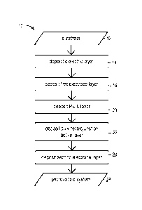
[0010] Figure 1 is a flowchart diagram illustrating a bottom up process for
producing a photovoltaic system according to the present invention, wherein
the order
of the bottom up deposition steps reads from the top down in the diagram;
[0011] Figure 2 is a flowchart diagram illustrating a bottom up process for
producing a photovoltaic system according to the present invention, wherein
the order
of the bottom up deposition steps reads from the top down in the diagram;
[0012] Figure 3 is a flowchart diagram illustrating a bottom up process for
producing a photovoltaic system according to the present invention, wherein
the order
of the bottom up deposition steps reads from the top down in the diagram;
[0013] Figure 4 is a schematic diagram illustrating a photovoltaic system
according to the present invention produced in accordance with the process
illustrated
in Figure 1;
[0014] Figure 5 is a schematic diagram illustrating a photovoltaic system
according to the present invention produced in accordance with the process
illustrated
in Figure 2;
[0015] Figure 6 is a schematic diagram illustrating a photovoltaic system
according to the present invention produced in accordance with the process
illustrated
in Figure 3; and
[0016] Figure 7 is a schematic diagram illustrating another photovoltaic
system according to the present invention.
3
CA 02930385 2016-05-11
WO 2015/073542
PCT/US2014/065227
[0017] The reader will appreciate the foregoing details, as well as others,
upon considering the following detailed description of the processes and
systems
according to this specification.
DESCRIPTION
[0018] As described in this specification the present invention is directed to
processes for producing low work function electrodes for organic photovoltaic
systems, such as, for example, polymer-fullerene bulk heterojunction organic
photovoltaic systems. The processes may comprise depositing an electrode layer
onto
a substrate and spray coating an ethoxylated polyethyleneimine (PETE) layer
onto the
electrode layer. This multi-layer spray coating process avoids the functional
surface
area constraints imposed by other deposition techniques, such as spin coating,
for
example, and may be used to produce large-area organic photovoltaic systems
with
relatively high through-put.
[0019] As used in this specification, including the claims, the term
"work
function" refers to the minimum energy required to remove an electron from a
solid
material to a point immediately adjacent to the solid material surface. In the
active
material of an organic photovoltaic system, a photo-excited electron
dissociated from
its corresponding hole in the semiconducting polymer occupies the LUMO energy
level of the acceptor material (e.g., a fullerene compound). Therefore, the
work
function of the cathode in an organic photovoltaic system must be sufficiently
low in
order to approximate the LUMO energy level of the acceptor material and
extract/collect the electron from the active material. On the other hand, the
work
function of the anode in an organic photovoltaic system must be relatively
higher than
the work function of the cathode to provide the driving force for exciton
dissociation,
transport, and the extraction/collection of holes.
[0020] The cathodes and anodes in organic photovoltaic systems are
generally comprised of different materials having different work functions.
Electrodes must also be sufficiently conductive to establish an electric
current. Many
conductive metals such as silver and conductive polymers such as blends of
poly(3,4-
ethylenedioxythiophene) : poly(styrene sulfonate) (PEDOT:PSS) possess the
necessary intrinsic electrical conductivity, but the intrinsic work function
of such
materials is too high to function effectively as a cathode in organic
photovoltaic
4
systems. The processes described in this specification address and overcome
these
problems by spray coating an ethoxylated polyethyleneimine (PEIE) layer onto
an
electrode layer to reduce the work function of the electrode layer, thereby
making the
electrode material suitable for use as a cathode in an organic photovoltaic
system. In
this manner, the anode in an organic photovoltaic system may comprise a
material
such as, for example, silver or a PEDOT:PSS-based polymeric composition, and
the
corresponding cathode may comprise the same material or a different material
with a
spray-coated PPIE Layer located between and contacting the cathode and the
active
material, wherein the ['FIE layer lowers the work function of the cathode.
[0021] Ethoxylated polyethyleneimine (PEIF,) is a highly branched
copolymer comprising primary and secondary amino groups and having the
following
general chemical structure:
OH
õN.
- Aka N
H
x
FN. ,01-1
HO' N
-OH
wherein x, y, and z indicate the repeating units of the copolymer. PDF
functions as a
surface modifier, reducing the work function of an electrode when applied to
the
surface of the electrode. Without intending to be bound by any theory, it is
believed
that the amine groups in PEIE molecules arc primarily involved in surface
interactions
with electrode material, giving rise to interface dipoles that reduce the work
function
but do not change the electrical transmittance between the active material and
a PEIE-
modified electrode in an organic photovoltaic system.
[0022] The work function modifying properties of PEIE are
described, for
example, in Zhou et al., Science, vol. 336, pp. 327-332 (2012) and
International Patent
Application Publication No. WO 2012/166366 Al.
CA 2930385 2017-09-15
These references disclose spin coating PEIE layers
onto electrode surfaces. Spin coating is a batch process requiring the usc of
specialized equipment that spins the deposition substrate to spread the
coating
material by centrifugal force. Spin coating therefore severely limits the
surface area
over which material may bc deposited and the rate of photovoltaic device
production_
The processes described in this specification employ spray coating techniques
to
deposit PEIE layers and preferably also other layers comprised in photovoltaic
systems according to the present invention. Spray coating avoids the
functional
surface area constraints imposed by other deposition techniques such as spin
coating.
Spray coating may also be used to produce large-area organic photovoltaic
systems
with relatively high through-put, making the processes described in this
specification
useful for the mass production of photovoltaic systems at higher rates.
[0023] As used in this specification, including the claims, "spray
coating"
refers to a coating process comprising atomizing or aerosolizing a liquid
coating
composition in a compressed gas stream functioning as a carrier medium that
propels
the coating composition, targeting the carrier gas comprising the coating
composition
into contact with a substrate, and depositing the coating composition from the
carrier
gas stream onto the substrate forming a coating layer. As used in this
specification,
including the claims, "spray coating" also includes eleetro-spray coating in
which a
liquid coating composition is atomized or-aerosolized and propelled into
contact with
a substrate (where the coating composition deposits onto the substrate forming
a
coating layer) using electrical charge as the driving mechanism, with or
without a
gaseous carrier medium. The spray coating of PEIE layers and optionally other
layers
comprised in a photovoltaic system may be performed manually using a hand-held
spray gun or automated using a computer-controlled robotic spray coating
system.
[0024] According to the present invention, a PEIE layer may be
spray
coated onto the surface of an electrode to be located adjacent to the
photoelectric
active material in an organic photovoltaic system. The PEIE material may be
pray
coated using an aqueous solution and dried to form a layer having a dry film
thickness
in the range of I nanometer to 50 nanometers, or any sub-range subsumed
therein,
such as, for example, 10-30 nanometers or 10-20 nanometers. The thickness and
density of a spray coated PEIE layer may be controlled by setting the spray
coating
6
CA 2930385 2017-09-15
CA 02930385 2016-05-11
WO 2015/073542
PCT/US2014/065227
process parameters, including the geometry of the spraying nozzle, the
distance
between the spray nozzle and the electrode surface, the composition of the
carrier gas
(e.g., air, nitrogen, argon, and the like), the flow rate of the carrier gas,
the pressure of
the carrier gas, the temperature of the electrode surface target, the
temperature of the
PEIE coating solution, the composition of the PEIE coating solution (e.g.,
solvent
composition, PEIE concentration, and the like), the lateral trajectory of the
spray
nozzle, the duration of the spray contact with the electrode target, and the
number of
spray coats applied to the electrode target. The process parameters used to
achieve a
PEIE layer of specified thickness and density may depend on the surface
texture
properties of the adjacent layer onto which the PEIE layer is deposited.
[0025] A PEIE layer may for example be spray coated in accordance with
the present invention using an aqueous formulation comprising 0.10% to 10.00%
PEIE by weight based on the total weight of the formulation, or any sub-range
subsumed therein, such as, for example 0.40-5.00% by weight based on the total
weight of the formulation. The aqueous formulation may be substantially free
of
alcohols such as methoxyethanol, which means that such compounds, if present
at all,
are present in the aqueous formulation at no greater than incidental impurity
levels.
The aqueous formulation used for spray coating a PEIE layer according to the
present
invention may include a non-toxic alcohol co-solvent or additive such as, for
example,
ethanol or isopropanol. The aqueous formulation for spray coating a PEIE layer
used
in accordance with the present invention may consist of PEIE and water.
Alternatively, the aqueous formulation for spray coating a PEIE layer may
consist of
PEIE, water, and isopropanol, for example, or may consist of PEIE, water, and
ethanol, for example.
[0026] According to the present invention an electrode layer may be spray
coated onto a substrate and a PEIE layer may be spray coated onto the
electrode layer
to produce a low work function electrode for a photovoltaic system. For
example, an
electrode layer comprising a conductive polymer may be spray coated onto a
substrate. A formulation comprising poly(3,4-ethylenedioxythiophene) :
poly(styrene
sulfonate) (PEDOT:PSS) may be spray coated onto a substrate to produce a
PEDOT:PSS-based polymeric electrode layer. The PEDOT:PSS-containing
formulation may, for example, be spray coated using an aqueous dispersion and
dried
7
to form a layer having a dry film thickness in the range of 150 nanometers to
250
nanometcrs, or any sub-range subsumed therein, such as, for example, 180-230
nanometers: PEDOT:PSS-hased polymeric electrodes exhibit an intrinsic work
function of about 4.96 + 0.06 eV. A PEDOT:PSS-based polymeric electrode layer
having a spray coated PEIE layer on a surface of the electrode layer may
exhibit a
reduced work function of about 3.5/. 0.06 eV.
[0027] The PEDOT:PSS-based polymeric electrode layer may, for
example,
be formed by spray coating an aqueous dispersion formulation comprising
poly(3,4-
ethylenedioxythiopherre); poly(styrene sulfonate); and one or more than one of
ethylene glycol or ditriethyl sulfoxide. This formulation is referred to
herein as
"PEDOT:PSS PH1000." The PEDOT:PSS PH1000 formulation may, for example,
comprise 1.0% to 1.3% solids content by weight, based on the total weight of
the
formulation, and a PEDOT:PSS ratio of 1:2.5 by weight. PEDOT:PSS P111000
formulations without ethylene glycol or dimethyl sulfoxide may be obtained,
for
example, from Heraeus Conductive Polymers under the trade name CLEVIOS. For
example, without being limited thereto, 4-8% by weight ethylene glycol and/or
dimethyl sulfoxide, based on total weight of the formulation, may be added to
such
commercially available formulations to produce PEDOT:PSS PH1000 formulations
that may be used in accordance with the present. invention,
[0028] According to the present invention also metallic lavers and
in
particular silver layers can be used as electrode layers. For example, a
silver layer
may be spray coated onto a substrate to produce a silver electrode layer.
Metallic
silver layers may be spray coated in accordance with a Tollcns' reaction in
which
silver nitrate in an aqueous ammonia solution is reduced to silver metal
during the
spraying by reaction with an aldehyde-containing compound. The spray coating
of
metallic silver layers is generally described, for example, in European Patent
Publication Nos. 0 346 954 A2 and 1 469 099 Al.
An aqueous ammonia and silver nitrate solution may
be loaded into a First chamber of a dual-spray gun, and an aqueous solution of
an
aldehyde-containing compound may be loaded into a second chamber of the dual-
spray gun. The two solutions are then mixed immediately before exiting the
spray
gun and the reagents react during the spray deposition process, thereby
forming a
8
CA 2930385 2017-09-15
CA 02930385 2016-05-11
WO 2015/073542
PCT/US2014/065227
silver layer on a target substrate from the reaction products of the Tollens'
reaction.
A spray coated silver electrode layer may, for example, have a dry film
thickness in
the range of 50 nanometers to 150 nanometers, or any sub-range subsumed
therein,
such as, for example, 50-75 nanometers. Metallic silver exhibits an intrinsic
work
function of about 4.60 0.06 eV. A silver electrode layer having a spray
coated PE1E
layer on a surface of the electrode layer may exhibit a reduced work function
of about
3.70 0.06 eV.
[0029] According to the present invention, an electrode layer may comprise
a layer of dielectric material comprising metallic particles embedded in the
dielectric
material. For example, an electrode layer may comprise a polyurethane-based
clear
coat composition comprising micron-scale or nano-scale metallic particles
embedded
in the cured clear coat composition. The metallic particles may comprise
copper
particles, gold particles, platinum particles, and/or silver particles, for
example. The
metallic particles may comprise a core-shell structure comprising a copper
core
particle encapsulated with silver shell layer. By way of example, copper-
silver core-
shell particles having a mean particle size of about 5-15 micrometers (for
example, 12
micrometers) may be mixed into the resin component of a two-component urethane
clear coating composition such as D8122 available from PPG Industries, Inc.
The
particles may be added to the resin component at a concentration of 40% to 60%
by
weight (for example, 50%) and stirred for a period of time, such as, for
example, 10
minutes, to ensure that the particles are dispersed in the resin component.
The resin
component having dispersed particles may be mixed with a hardener component
and,
optionally, diluted with a solvent to a viscosity suitable for spray coating
of an
electrode layer comprising metallic particles embedded in a cured dielectric
material
(14-16 dyn-second per square centimeter, for example). The curing conditions
(temperature, time, and the like) of the spray coated electrode will depend on
the
particular dielectric material used. Suitable dielectric materials include,
for example,
cured polymer clear-coats such as acrylic, urethane, and epoxy based
formulations.
[0030] The electrode and PETE layers may be respectively deposited onto a
surface of any substrate that is or can be exposed to sunlight, such as, for
example,
buildings, vehicles, modular panels, photovoltaic device substrates, and the
like. The
spray coating techniques used in the processes according to the present
invention
9
CA 02930385 2016-05-11
WO 2015/073542
PCT/US2014/065227
enable the production of photovoltaic coating systems comprising a stack of
spray
coated layers, including an electrode layer and a PETE layer, that together
form a
functional photovoltaic system deposited onto any convenient or suitable
substrate.
The substrate may, for example, comprise an electrically insulating dielectric
layer
that may be deposited onto an underlying substrate material to provide a
homogenous
and continuous base layer that is electrically, chemically, and mechanically
inert to
the overlying functional photovoltaic layers. The dielectric layer may provide
a non-
porous and relatively planar base layer. Typically the dielectric base layer,
if present,
has a surface roughness of less than 25 nanometers (Ra), preferably of less
than 20
nanometers (Ra), more preferably of less than 15 nanometers (Ra), even more
preferably of less than 10 nanometers (Ra), or less than 5 nanometers (Ra).
[0031] Such optionally present inert, non-porous, and relatively planar
dielectric layer may, for example, comprise a cured acrylic urethane clear-
coat layer.
As used herein the term "cured," refers to the condition of a liquid coating
composition in which a film or layer formed from the liquid coating
composition is at
least tack free to touch. As used herein, the terms "cure" and "curing" refer
to the
progression of a liquid coating composition from the liquid state to a cured
state and
encompass physical drying of coating compositions through solvent or carrier
evaporation (e.g., thermoplastic coating compositions) and/or chemical
crosslinking
of components in the coating compositions (e.g., thermosetting coating
compositions).
An example of a suitable acrylic urethane clear-coating composition that may
be used
to form a dielectric layer on a substrate is the D8109 UHS Clearcoat available
from
PPG Industries, Inc. As an example, an epoxy primer composition may be used to
form an epoxy primer layer on a substrate, and an acrylic urethane clear-
coating
composition may be used to form a dielectric layer deposited on the underlying
epoxy
primer layer. According to the present invention, a dielectric layer may be
spray
coated onto a substrate, and the electrode and PETE layers may be respectively
spray
coated onto the dielectric layer. A spray coated dielectric layer may have any
dry film
thickness, provided the dielectric layer provides a base layer with
sufficiently low
surface roughness (less than 25 nanometer Ra, for example).
[0032] The processes for producing low work function electrodes described
in this specification may be incorporated into processes for producing
photovoltaic
CA 02930385 2016-05-11
WO 2015/073542
PCT/US2014/065227
systems. Figure 1 illustrates a process 10 for producing a photovoltaic system
in
accordance with the present invention. A substrate is provided at step 12. The
substrate may comprise any substrate that is or can be exposed to sunlight,
such as,
for example, buildings, vehicles, modular panels, photovoltaic device
substrates, and
the like. A dielectric layer is then deposited onto the substrate at step 14.
The
dielectric layer may comprise a spray coated layer, as described above. For
example,
the dielectric layer may comprise a spray coated layer comprising a cured
acrylic
urethane clear-coat or a combination of an underlying epoxy primer layer and
an
overlying acrylic urethane clear-coat layer. A first electrode layer is
subsequently
deposited onto the dielectric layer at step 16. The first electrode layer may
comprise a
spray coated layer, as described above. For example, the first electrode layer
may
comprise a spray coated PEDOT:PSS PH1000 layer, a spray coated silver layer
formed from the reaction products of a Tollens' reaction, or a spray coated
layer of
dielectric material comprising metallic particles embedded in the dielectric
material.
A PElE layer is deposited onto the first electrode layer at step 20. The PElE
layer can
be spray coated onto the first electrode layer, as described above.
[0033] A bulk heterojunction active layer is then deposited onto the PElE
layer at step 22 of the process illustrated in Figure 1. The bulk
heterojunction active
layer may comprise an organic, semiconducting, low band gap polymer that
functions
as an electron donor when contacted with visible light. Typically the bulk
heterojunction active layer comprises a blend comprising an organic,
semiconducting,
low band gap polymer and an electron acceptor compound. For example, the bulk
heterojunction active layer may comprise a blend of poly(3-hexyl thiophene)
and
[6,6]-phenyl C61-butyric acid methyl ester (P3HT:PCBM). Other low band gap
polymers suitable for the bulk heterojunction active layer include, for
example,
poly[[4,8-bis[(2-ethylhexyl)oxy]benzo[1,2-b:4,5-bldithiophene-2,6-diyl][3-
fluoro-2-
[(2-ethylhexyl)carbonyl]thieno[3,4-b]thiophenediyl]] (PTB7). PTB7 has the
following general chemical structure:
11
CA 02930385 2016-05-11
WO 2015/073542
PCT/US2014/065227
S
a
- n
F-=
ROCK:
wherein R is a 2-ethylhexyl group and n denotes the repeating units of the
polymer.
Other suitable low band gap polymers include, but are not limited to, poly[2,6-
(4,4-
bis-(2-ethylhexyl)-4H-cyclopenta [2,1-b;3,4-b']dithiophene)-alt-4,7(2,1,3-
benzothiadiazole)] (PCPDTBT), which has the following general chemical
structure
(n denotes the repeating units of the polymer):
S.
-/1
/
' N\
x4,
H36 CH3 n
1
CH3
H36
and poly[2,1,3-benzothiadiazole-4,7-diy1[4,4-bis(2-ethylhexyl)-4H-silolo[3,2-
b:4,5-
b]dithiophene-2,6-diyl]] (Si-PCPDTBT), which has the following general
chemical
structure (n denotes the repeating units of the polymer):
12
"
S.
;
:=
I .....
,
"0.
I 'S.
v. 41
11
In addition of the photoactive polymers described above, it is understood that
the
processes and systems described in this specification can use any suitable
photoactive
low band gap polymers that produce electron-hole pairs when blended with an
electron acceptor compound such as, for example, a fullerene compound, in a
bulk
hetero junction active layer exposed to light. Low band gap polymers may be
used to
achieve improved photovoltaic efficiency (n).
[0034] The bulk heterojunction active layer may be spray coated onto the
PETE layer. The spray coating of bulk heterojunction active layers is
described, for
example, in U.S. Patent Application Publication No. 2009/0155459 Al.
The bulk hetcrojunction active layer
may, for example, be spray coated onto the PETE layer using solutions of low
band
gap electron donor polymers and electron acceptor compounds, as defined above,
in
chlorinated solvents or non-chlorinated solvents. For example, low band gap
electron
donor polymers and electron acceptor compounds can be dissolved in chlorinated
solvents such as, for example, I -chloronaphthalene, chlorobenzenes, di-
chlorobenzencs, and mixtures or any thereof. Alternatively, low band gap
electron
donor polymers and electron acceptor compounds can be dissolved in non-
chlorinated
solvents such as, for example, ortho-xylene, para-xylene, ortho- and para-
xylene
blends, other x ylcnc blends, tctrahydrothiophene, anisolc, and mixtures of
any
thereof. Other co-solvents and additives that may be added to any non-
chlorinated
solvent used to dissolve low band gap electron donor polymers and electron
acceptor
compounds can include, hut are not limited to, dimethylnaphthalene, terpineol,
and/or
1,8-dilodooetane (D10). A spray coated active layer may typically have a dry
film
13
CA 2930385 2017-09-15
CA 02930385 2016-05-11
WO 2015/073542
PCT/US2014/065227
thickness in the range of 180 nanometers to 240 nanometers, or any sub-range
subsumed therein, such as, for example, 200-220 nanometers.
[0035] A second electrode layer is then deposited onto the active layer at
step 26 of the process according to Figure 1. The second electrode layer can
be any
electrode layer as defined above in the context of the first electrode layer.
Thus it
may, for example, comprise a spray coated electrode layer, as described above.
For
example, the second electrode layer may comprise a spray coated PEDOT:PSS
PH1000 layer or a spray coated silver layer such as a silver layer formed from
the
reaction products of a Tollens' reaction. The second electrode layer may, for
example, comprise a blend of PEDOT:PSS PH1000 and a second PEDOT:PSS-based
polymeric material, such as, for example, a PEDOT:PSS-based polymeric material
comprising poly(3,4-ethylenedioxythiophene), poly(styrene sulfonate), N-methy1-
2-
pyrrolidone, a gamma-glycidoxypropyltrimethoxysilane crosslinking agent,
isopropanol, and an acetylenic glycol-based nonionic surfactant. This
formulation is
referred to in this specification, including the claims, as "PEDOT:PSS CPP."
[0036] The second electrode layer should be at least partially transparent to
light in order for incident light to transmit through the second electrode
layer and
enter into the bulk heterojunction active layer. A second electrode layer
comprising a
spray coated silver layer may, for example, have a dry film thickness in the
range of
25 nanometers to 75 nanometers, or any sub-range subsumed therein, such as,
for
example, 50-60 nanometers. A second electrode layer comprising a spray coated
PEDOT:PSS PH1000 layer, or a spray coated layer comprising a blend of
PEDOT:PSS PH1000 and PEDOT:PSS CPP, may, for example, have a dry film
thickness in the range of 100 nanometers to 200 nanometers, or any sub-range
subsumed therein, such as, for example, 160-180 nanometers.
[0037] A complete photovoltaic system is provided at step 28 of the process
depicted in Figure 1 after the serial deposition of the aforementioned layers.
Figure 4
schematically illustrates a photovoltaic system 110 produced according to the
process
illustrated in Figure 1. The photovoltaic system 110 comprises the following
layers
stacked in the following order starting from the substrate 112 at the bottom:
a
dielectric layer 114 over the substrate 112, a first electrode layer 116 over
the
dielectric layer 114, a PETE layer 120 over the first electrode layer 116, a
bulk
14
CA 02930385 2016-05-11
WO 2015/073542
PCT/US2014/065227
heterojunction active layer 122 over the PEIE layer 120, and a second
electrode layer
126 over the bulk heterojunction active layer 122. The constituting layers may
each
be as described above. The first and second electrode layers 116 and 126 may
thus
independently comprise, for example, a PEDOT:PSS PH1000 layer and/or a silver
layer. The second electrode layer 126 may, for example, comprise a blend of
PEDOT:PSS PH1000 and PEDOT:PSS CPP. The first electrode layer 116 may
comprise a dielectric material comprising metallic particles embedded in the
dielectric
material. The bulk heterojunction active layer 122 may, for example, comprise
a
P3HT:PCBM layer, PTB7:PCBM layer, a PCPDTBT:PCBM layer, or a Si-
PCPDTBT:PCBM layer.
[0038] In the photovoltaic system 110, the first electrode layer 116
generally
has a lower work function than the second electrode layer 126, even if these
two
electrode layers are made of the same material (e.g., PEDOT:PSS PH1000 or
silver),
because of the PETE layer 120 located between and in contact with the first
electrode
layer 116 and the active layer 122. The first electrode layer 116 functions as
a
cathode and the second electrode layer 126 functions as an at least partially
transparent anode. The at least partial transparency of the second electrode
layer 126
is necessary for incident light to enter into the active layer 122 and produce
excitons
that dissociate into electrons (collected through the cathode layer 116) and
holes
(collected through the anode layer 126).
[0039] Figure 2 illustrates another process 30 for producing a photovoltaic
system according to the present invention. The process 30 illustrated in
Figure 2 is
similar to the process 10 illustrated in Figure 1, but comprises an additional
step 44.
A substrate is provided at step 32. The substrate may comprise any suitable
substrate
as defined above. A dielectric layer is then deposited onto the substrate at
step 34.
The dielectric layer may, for example, comprise a spray coated layer, as
described
above. For example, the dielectric layer may comprise a spray coated layer
comprising a cured acrylic urethane clear-coat or a combination of an
underlying
epoxy primer layer and an overlying acrylic urethane clear-coat layer. A first
electrode layer is subsequently deposited onto the dielectric layer at 36. The
first
electrode layer may, for example, comprise a spray coated layer, as described
above.
For example, the first electrode layer may comprise a spray coated PEDOT:PSS
P141000 layer, a spray coated silver layer formed from the reaction products
of a
Tollens' reaction, or a spray coated layer of dielectric material comprising
metallic
particles embedded in the dielectric material. A ['FIE layer is deposited onto
the first
electrode layer at step 40. The PEIE layer is spray coated onto the first
electrode
layer, as described above.
[0040] A bulk heterojunction active layer is then deposited onto
the PEIE
layer at step 42. The bulk heterojunction active layer may comprise a blend
comprising an organic semiconducting polymer (functioning as an electron
donor)
and an electron acceptor compound. For example, the bulk hetcrojunction active
layer may comprise a blend of poly(3-11exyl thiophene) and [6,6]-phenyl C6J-
butyric
acid methyl ester (P31-iT:PCBM), or the bulk heteroj unction active layer may
comprise a PTB7:PCBM blend, a PCPDTBT:PCBM blend, or a Si-PCPDTBT:PCBM
blend, The bulk heterojunction active layer may be spray coated onto the PEIE
layer
as described above in connection with Figure I. The spray coating of organic
photovoltaic active layers is described, for example, in U.S. Patent
Application
Publication No. 2009/0155459 Al.
[0041] A PEDOT:PSS-based polymeric layer is deposited onto the active
layer at step 44. This layer may comprise a hole transport layer. In some
aspects, the
PEDOT:PSS-based polymeric layer may be spray coated onto the active layer at
44
using a formulation comprising poly(3,4-ethylenedioxythiophene), poly(styrene
sulfonate), N-methy1-2-pyrrolidone, a gamma-glycidoxypropyltrimethoxysilanc
crosslinking agent, isopropanot, and an acetylenic glycol-based nonionic
surfactant
As described above, this formulation is referred to in this specification,
including the
claims, as "PEDOT:PSS CPP."
[0042] heterojunetion active layers comprising P3HT:PCBM or
PTB7:PCBM, for example, may exhibit poor aqueons \vetting properties that may
result in insufficient adhesion and electrical conductance between the active
layers
and overlying electrode layers deposited from aqueous solutions (e.g., spray
coated
PEDOT:PSS PH1000 formulations and silver layers produced using sprayed Tol
lens'
reagents). PEDOT:PSS CPP formulations comprising poly(3,4-
ethylenedioxythiophenc), poly(styrenc sullonate), N-methyl-2-pyrrolidonc, a
gamma-
16
CA 2930385 2017-09-15
CA 02930385 2016-05-11
WO 2015/073542
PCT/US2014/065227
glycidoxypropyltrimethoxysilane crosslinking agent, isopropanol, and an
acetylenic
glycol-based nonionic surfactant exhibit better wetting on bulk heterojunction
active
layers, particularly P3HT:PCBM-based, PTB7:PCBM-based, PCPDTBT:PCBM-
based, or a Si-PCPDTBT:PCBM-based active layers. PEDOT:PSS CPP layers
deposited from this formulation also have a different morphology than films
formed
from other PEDOT:PSS formulations, such as PEDOT:PSS PH1000, resulting in
improved electrical conductance between underlying active layers and overlying
electrode layers. The PEDOT:PSS CPP layer spray coated or otherwise deposited
at
step 44 may, for example, have a dry film thickness in the range of 75
nanometers to
125 nanometers, or any sub-range subsumed therein, such as, for example, 90-
100
nanometers. A second electrode layer is deposited onto the PEDOT:PSS CPP layer
at
step 46. The second electrode layer may comprise a spray coated layer, as
described
above. For example, the second electrode layer may comprise a spray coated
PEDOT:PSS PH1000 layer or a spray coated silver layer formed from the reaction
products of a Tollens' reaction. Alternatively, the second electrode layer may
comprise a blend of PEDOT:PSS PH1000 and PEDOT:PSS CPP.
[0043] A complete photovoltaic system is provided at step 48 of the process
depicted in Figure 2 after the serial deposition of the layers. Figure 5
schematically
illustrates a photovoltaic system 130 produced according to the process
illustrated in
Figure 2. The photovoltaic system 130 comprises the following layers stacked
in the
following order starting from the substrate 132 at the bottom: a dielectric
layer 134
over the substrate 132, a first electrode layer 136 over the dielectric layer
134, a PETE
layer 140 over the first electrode layer 136, a bulk heterojunction active
layer 142
over the PETE layer 140, a PEDOT:PSS CPP hole transport layer 144 over the
bulk
heterojunction active layer 142, and a second electrode layer 146 over the
PEDOT:PSS CPP hole transport layer 144. The constituting layers may each be as
described above. The first and second electrode layers 136 and 146 may thus
independently comprise, for example, a PEDOT:PSS PH1000 layer and/or a silver
layer. The second electrode layer 146 may comprise a blend of PEDOT:PSS PH1000
and PEDOT:PSS CPP. The first electrode layer 136 may comprise a dielectric
material comprising metallic particles embedded in the dielectric material.
The bulk
heterojunction active layer 142 may, for example, comprise a P3HT:PCBM layer,
a
PTB7:PCBM layer, a PCPDTBT:PCBM layer, or a Si-PCPDTBT:PCBM layer.
17
CA 02930385 2016-05-11
WO 2015/073542
PCT/US2014/065227
[0044] In the photovoltaic system 130, the first electrode layer 136 generally
has a lower work function than the second electrode layer 146, even if these
two
electrode layers are made of the same material (e.g., PEDOT:PSS PH1000 or
silver),
because of the PETE layer 140 located between and in contact with the first
electrode
layer 136 and the active layer 142. The first electrode layer 136 functions as
a
cathode and the second electrode layer 146 functions as an at least partially
transparent anode. The PEDOT:PSS CPP hole transport layer 144 functions as an
at
least partially transparent hole transport layer. The at least partial
transparency of the
second electrode layer 146 and the PEDOT:PSS CPP hole transport layer 144 is
necessary for incident light to enter into the active layer 142 and produce
excitons that
dissociate into electrons (collected through the cathode layer 136) and holes
(collected
through the hole transport layer 144 and the anode layer 146).
[0045] Figure 3 illustrates another process 50 for producing a photovoltaic
system according to the present invention. The process 50 illustrated in
Figure 3 is
similar to the process 30 illustrated in Figure 2, but comprises an additional
step 58.
A substrate is provided at step 52. The substrate may comprise any substrate
that is or
can be exposed to sunlight, such as, for example, buildings, vehicles, modular
panels,
photovoltaic device substrates, and the like, as described above. A dielectric
layer is
then deposited onto the substrate at step 54. The dielectric layer may e.g.
comprise a
spray coated layer, as described above. For example, the dielectric layer may
comprise a spray coated layer comprising a cured acrylic urethane clear-coat
or a
combination of an underlying epoxy primer layer and an overlying acrylic
urethane
clear-coat layer. A first electrode layer is subsequently deposited onto the
dielectric
layer at step 56. The first electrode layer may, for example, comprise a spray
coated
layer, as described above. For example, the first electrode layer may comprise
a spray
coated PEDOT:PSS PH1000 layer, a spray coated silver layer such as a silver
layer
formed from the reaction products of a Tollens' reaction, or a spray coated
layer of
dielectric material comprising metallic particles embedded in the dielectric
material.
[0046] A lower work function metallic layer is then deposited onto the first
electrode layer at step 58. The lower work function metallic layer may
comprise a
metal such as, for example, titanium or chromium. A lower work function
metallic
layer (such as a titanium layer or a chromium layer) may be deposited onto the
first
18
electrode by vacuum thermal evaporation-deposition or cold spraying. For
example_
The lower work function metallic layer deposited at 58 may, for example, have
a dry
film thickness in the range of 5 nanoineters 1o,25 nanometers, or any sub-
range
'subsumed therein, such as, for example, 10-20 nanometers.
[0047] A PEIE layer is then deposited onto the lower work function
metallic
layer at step 60. The PEIE layer may be spray coated onto the lower work
function
metallic layer in the same manner described above in which a PEIE layer is
spray
coated onto an electrode layer. A bulk heterojunetion active layer is then
deposited
onto the PEIE layer at step 62. The bulk heterojunction active layer may, for
example, comprise a blend comprising an organic semiconducting polymer
(functioning as an electron donor) and an electron acceptor compound. For
example,
the bulk lietcrojunetion active layer may comprise a blend of poly(3-hcxyl
thiophene)
and 16,61-phenyl Col-butyric acid methyl ester (P31IT:PCBM), or the bulk
lieterojunction active layer may comprise a PTB7:PCBM blend, a PCPDTBT:PCBM
blend, or a Si-PCPDTBT:PCBM blend, The bulk heterojunction active layer may be
spray coated onto the PEIE layer as described above in connection with Figures
I and
2. The spray coating of organic photovoltaic active layers is described, for
example,
in U.S. Patent Application Publication No. 2009/0155459 At.
[0048] A PEDOT:PSS CPP hole transport layer is then deposited onto
the
active layer at step 64. The PEDOT:PSS CPP hole transport layer may, for
example,
be spray coated onto the active layer using a formulation comprising poly(3,4-
cthylenedioxythiophene), poly(styrene sulfonate), N-methyl-2-pyrrolidone, a
gamma-
glycidoxypropyltrimethoxysilane crosslinking agent, isopropanol, and an
acetylenie
glycol-based nonionic surfactant, as described above in connection with Figure
2. A
second electrode layer is then deposited onto the PEDOT:PSS CPP hole transport
layer at step 66. The second electrode layer may, for example, comprise a
spray
coated layer, as described above. For example, the second electrode layer may
comprise a spray coated PEDOT:PSS P1-11000 layer or a spray coated silver
layer
such as a silver layer formed from the reaction products of a Tollens'
reaction.
According to the present invention the second electrode layer may also
comprise a
blend of PEDOT:PSS P1-11000 and PEDOT:PSS CPR
19
CA 2930385 2017-09-15
CA 02930385 2016-05-11
WO 2015/073542
PCT/US2014/065227
[0049] A complete photovoltaic system is provided at step 68 of the process
depicted in Figure 3 after the serial deposition of the aforementioned layers
in steps
54-66. Figure 6 schematically illustrates a photovoltaic system 150 produced
according to the process illustrated in Figure 3. The photovoltaic system 150
comprises the following layers stacked in the following order starting from
the
substrate 152 at the bottom: a dielectric layer 154 over the substrate 152, a
first
electrode layer 156 over the dielectric layer 154, a lower work function
metallic layer
158 over the first electrode layer 156, a PEIE layer 160 over the lower work
function
metallic layer 158, a bulk heterojunction active layer 162 over the PEIE layer
160, a
PEDOT:PSS CPP hole transport layer 164 over the bulk heterojunction active
layer
162, and a second electrode layer 166 over the PEDOT:PSS CPP hole transport
layer
164. The constituting layers may each be as described above. The first and
second
electrode layers 156 and 166 may thus independently comprise, for example, a
PEDOT:PSS PH1000 layer and/or a silver layer. The second electrode layer 166
may
comprise a blend of PEDOT:PSS PH1000 and PEDOT:PSS CPP. The first electrode
layer 156 may comprise a dielectric material comprising metallic particles
embedded
in the dielectric material. The bulk heteroj unction active layer 162 may
comprise a
P3HT:PCBM layer, a PTB7:PCBM layer, a PCPDTBT:PCBM layer, or a Si-
PCPDTBT:PCBM layer.
[0050] In the photovoltaic system 150, the lower work function metallic
layer 158 and the PEIE layer 160 function together as electron transport
layers that
conduct photo-excited and dissociated electrons from the active layer 162 to
the first
electrode layer 156. By functioning as electron transport layers, the lower
work
function metallic layer 158 and the PEIE layer 160 effectively lower the work
function of the first electrode layer 156, even if the first electrode layer
156 and the
second electrode layer 166 are made of the same material (e.g., PEDOT:PSS
PH1000
or silver). The first electrode layer 156 functions as a cathode and the
second
electrode layer 166 functions as an at least partially transparent anode. The
PEDOT:PSS CPP hole transport layer 164 functions as an at least partially
transparent
hole transport layer. The at least partial transparency of the second
electrode layer
166 and the PEDOT:PSS CPP hole transport layer 164 is necessary for incident
light
to enter into the active layer 162 and produce excitons that dissociate into
electrons
(collected through the electron transport layers 160 and 158 and the cathode
layer
156) and holes (collected through the hole transport layer 164 and the anode
layer
166).
[0051] Although not illustrated in Figures 1-6, it is understood
that
according to the present invention, optionally an inorganic hole transport
layer may be
spray coated or otherwise deposited onto the bulk heterot unction active layer
before
spray coating or otherwise depositing a PEDOT:PSS CPP hole transport layer, if
present, and the second electrode layer. For example, a carbon nanotube layer,
a
graphene layer, or a molybdenum trioxide (Mo0.) layer may be spray coated onto
the
bulk heterojunetion active layer to form an inorganic hole transport layer
before spray
coating or otherwise depositing a PEDOT:PSS CPP hole transport layer, if
present,
and the second electrode layer (e.g., a silver layer, a PEDOT:PSS PHI 000
layer, or a
layer comprising a combination of PEDOT:PSS PH 1000 and PEDOT:PSS CPP). The
spray coating of molybdenum trioxide layers, for example, is described in
Suzuki et
al., "Electrospraycd molybdenum trioxide aqueous solution and its application
in
organic photovoltaic cells," PLOS One, vol. 9, no. 8, August 2014.
[0052] Figure 7 schematically illustrates another photovoltaic
system 170
produced according to the present invention. The photovoltaic system 170
comprises
the following layers stacked in the following order starting from the
substrate 172 at
the bottom: a dielectric layer 174 over the substrate 172, a first electrode
layer 176
over the dielectric layer 174, a PEIE layer 180 over the first electrode layer
176, a
bulk heterojunction active layer 182 over the PETE layer 180, an inorganic
hole
transport layer 185 over the bulk heteroj unction active layer 182, and a
second
electrode layer 186 over the inorganic hole transport layer 184. The
constituting
layers may each be as described above. The first and second electrode layers
176 and
186 may thus independently comprise, for example, a PEDOT:PSS PHI 000 layer
and/or a silver layer. The second electrode layer 186 may alternatively
comprise a
blend of PEDOT:PSS P141000 and PEDOT:PSS CPP. The first electrode layer 176
may comprise a dielectric material comprising metallic particles embedded in
the
dielectric material. The bulk hcterojunction active layer 182 may, for
example,
comprise a P3HT:PCBM layer, a PTB7:PCBM layer, a PCPDTBT:PCBM layer, or a
Si -PCPDTBT:PCBM layer. The inorganic hole transport layer 185 may comprise a
21
CA 2930385 2017-09-15
CA 02930385 2016-05-11
WO 2015/073542
PCT/US2014/065227
molybdenum trioxide layer, a graphene layer, or a carbon nanotube layer, for
example.
[0053] In the photovoltaic system 170, the first electrode layer 176 has a
lower work function than the second electrode layer 186, even if these two
electrode
layers are made of the same material (e.g., PEDOT:PSS PH1000 or silver),
because of
the PETE layer 180 located between and in contact with the first electrode
layer 176
and the bulk heterojunction active layer 182. The first electrode layer 176
functions
as a cathode and the second electrode layer 186 functions as an at least
partially
transparent anode. The inorganic hole transport layer 185 functions as an at
least
partially transparent hole transport layer. The at least partial transparency
of the
second electrode layer 186 and the inorganic hole transport layer 185 is
necessary for
incident light to enter into the active layer 182 and produce excitons that
dissociate
into electrons (collected through the cathode layer 176) and holes (collected
through
the hole transport layer 185 and the anode layer 186).
[0054] It is understood that the layers shown in Figure 7 can all be deposited
by spray coating operations in a process for producing the photovoltaic system
170.
In addition, although not illustrated in Figure 7, it is understood that
according to the
present invention, an optional organic hole transport layer (such as the
PEDOT:PSS
CPP hole transport layer described in connection with Figures 2 and 5) can be
deposited between the inorganic hole transport layer 185 and the second
electrode
layer 186. In addition, although not illustrated in Figure 7, it is understood
that, an
optional lower work function metallic layers (such as a chromium or titanium
layer as
described in connection with Figures 3 and 6) can be deposited between the
first
electrode layer 176 and the PETE layer 180.
[0055] Although not illustrated in Figures 1-7, it is understood that
according to the present invention, the second electrode layers (e.g., second
electrode
layers 126, 146, 166, and 186) can comprise a hybrid bi-layer structure
comprising an
organic layer and an inorganic layer. The hybrid bi-layer structure can, for
example,
comprise an organic layer comprising a PEDOT:PSS PH1000 layer or a layer
comprising a combination of PEDOT:PSS PH1000 and PEDOT:PSS CPP, and an
inorganic layer comprising an at least partially transparent silver layer. The
organic
layer (e.g., PEDOT:PSS PH1000 and PEDOT:PSS CPP blend) of the hybrid second
22
CA 02930385 2016-05-11
WO 2015/073542
PCT/US2014/065227
electrode bi-layer may be in direct physical contact with an underlying bulk
heterojunction active material layer, or in direct physical contact with an
optional
underlying inorganic hole transport layer. The inorganic layer (e.g., silver)
of the
hybrid second electrode bi-layer may be in direct physical contact with the
organic
layer of the hybrid second electrode bi-layer. The entire hybrid second
electrode bi-
layer is at least partially transparent so that incident light can enter into
the active
layer and produce excitons that dissociate into electrons and holes.
[0056] Although not illustrated in Figures 1-7, it is understood that in
implementations where the second electrode layers (e.g., second electrode
layers 126,
146, 166, and 186) or the organic layer of a hybrid second electrode bi-layer
implementation comprise PEDOT:PSS PH1000 or a blend of PEDOT:PSS PH1000
and PEDOT:PSS CPP, the layers may further comprise metallic nanoparticles
embedded in the layers. For example, second electrode layers may comprise gold
nanoparticles, copper nanoparticles, platinum nanoparticles, and/or silver
nanoparticles embedded in PEDOT:PSS-based layers. According to the present
invention, the nanoparticles can, for example, have an average particle size
of less
than 1000 nanometers, such as 5-500 nanometers or 10-100 nanometers.
[0057] Although not illustrated in Figures 1-7, it is understood that
according to the present invention, an optional outer protective barrier layer
may be
deposited onto the second electrode, provided that any outer protective
barrier layer is
at least partially transparent. Like the base dielectric layer, described
above, an outer
protective barrier layer may be electrically, chemically, and mechanically
inert to the
underlying functional photovoltaic layers. An outer protective barrier layer
may
hermetically seal the underlying functional photovoltaic layers and provide
barrier
protection against moisture or other potentially harmful environmental agents.
An
outer protective barrier layer may possess certain properties, such as, for
example, a
water vapor transmission rate of less than 10-2 g/m2/day or less than 10-4
g/m2/day or
less than 10' g/m2/day. The outer protective barrier layer may moreover
possess an
oxygen transmission rate of less than 10' cm3/m2/day.
[0058] The processes described herein for producing low work function
electrodes and for producing photovoltaic systems may be used to produce a
fully-
sprayed photovoltaic system, wherein each layer comprising the photovoltaic
system
23
CA 02930385 2016-05-11
WO 2015/073542
PCT/US2014/065227
is deposited using a spray coating operation. For example, in the processes
illustrated
in Figures 1-3 and other implementations in accordance with the present
invention,
each deposition step may be a spray coating step, and each layer illustrated
in Figures
4-7 may be a spray coated layer. Additionally, although Figures 4-7 illustrate
each
layer as a continuous layer fully covering the immediately underlying layer,
it is
understood that the present invention also relates to implementations, wherein
any
overlying layer may not fully cover the immediately underlying layer. For
example,
the second electrode layers 126, 146, 166, and 186 in Figures 4-7 may be spray
coated
or otherwise deposited in a predetermined pattern that provides for improved
light
transparency to the underlying active material layers.
[0059] The processes illustrated in Figures 1-3 only show deposition (e.g.,
spray coating) steps. However, additional steps may be performed between any
two
successive deposition/spray coating steps. For example, after the deposition
or spray
coating of a layer comprising a dielectric material, the layer may be
subjected to
curing conditions for a period of time to cure the dielectric material before
the
subsequent deposition or spray coating of an overlying layer. After the spray
coating
of a P3HT:PCBM or PTB7:PCBM active layer, for example, the deposited layer may
be thermally annealed before the subsequent deposition of an inorganic hole
transport
layer, a PEDOT:PSS CPP layer, and/or a second electrode layer. For example, a
spray coated P3HT:PCBM or PT137:PCBM active layer may be thermally annealed
for about 20 minutes at about 120 C while maintaining a substrate temperature
of
about 40 C. As another example, after the spray coating of a PEDOT:PSS CPP
hole
transport layer, the deposited layer may be thermally annealed for 20 minutes
at about
120 C while maintaining a substrate temperature of about 75 C. As another
example,
after the spray coating of a PEDOT:PSS PH1000 layer, the deposited layer may
be
thermally annealed for 1 minute at about 150 C while maintaining a substrate
temperature of about 100 C.
[0060] A preferred process according to the present invention for producing
a fully-sprayed photovoltaic system comprises spray coating a first electrode
layer
onto a substrate, spray coating a PEIE layer onto the first electrode layer,
spray
coating a bulk heterojunction active layer onto the PETE layer, and spray
coating a
second electrode layer onto the bulk heterojunction active layer. The process
may
24
CA 02930385 2016-05-11
WO 2015/073542
PCT/US2014/065227
optionally further comprise spray coating a dielectric layer onto the
substrate, and
spray coating the first electrode layer onto the dielectric layer. The process
may
optionally further comprise spray coating a PEDOT:PSS CPP hole transport layer
onto the bulk heterojunction active layer, and spray coating the second
electrode layer
onto the PEDOT:PSS CPP hole transport layer. The process may optionally
further
comprise spray coating an inorganic hole transport layer onto the bulk
heterojunction
active layer, and spray coating the second electrode layer onto the inorganic
hole
transport layer. The process may optionally further comprise spray coating a
lower
work function metallic layer onto the first electrode layer, and spray coating
the PETE
layer onto the metallic layer. The process may also further comprise spray
coating an
outer protective barrier layer onto the second electrode layer.
[0061] Another preferred process according to the present invention for
producing a fully-sprayed photovoltaic system comprises spray coating a
dielectric
layer onto a substrate, spray coating a first silver layer onto the dielectric
layer, spray
coating a PETE layer onto the first silver layer, spray coating a P3HT:PCBM
layer or a
PTB7:PCBM layer onto the PETE layer, spray coating a PEDOT:PSS CPP hole
transport layer onto the P3HT:PCBM layer or PTB7:PCBM layer, and spray coating
a
second silver layer onto the PEDOT:PSS CPP hole transport layer. The process
may
further comprise spray coating a titanium layer or a chromium layer onto the
first
silver layer, and spray coating the PE1E layer onto the titanium or chromium
layer.
The process may optionally further comprise spray coating an outer protective
barrier
layer onto the second silver layer. This example process produces a fully-
sprayed
photovoltaic system comprising an at least partially transparent silver anode,
a
PEDOT:PSS CPP hole transport layer, a P3HT:PCBM or PTB7:PCBM bulk
heterojunction active layer, and a cathode layer comprising silver and having
a lower
work function than the silver anode resulting from the PETE layer located
between
and contacting the P3HT:PCBM or PTB7:PCBM bulk heterojunction active layer and
the cathode layer comprising silver (or the optional titanium or chromium
electron
transport layer).
[0062] Another preferred process according to the present invention for
producing a fully-sprayed photovoltaic system comprises spray coating a
dielectric
layer onto a substrate, spray coating a first PEDOT:PSS PH1000 layer onto the
CA 02930385 2016-05-11
WO 2015/073542
PCT/US2014/065227
dielectric layer, spray coating a PETE layer onto the first PEDOT:PSS PH1000
layer,
spray coating a P3HT:PCBM layer or a PTB7:PCBM layer onto the PETE layer,
spray
coating a PEDOT:PSS CPP hole transport layer onto the P3HT:PCBM layer or
PTB7:PCBM layer, and spray coating a second PEDOT:PSS PH1000 layer onto the
PEDOT:PSS CPP hole transport layer. In such process, the PEDOT:PSS CPP hole
transport layer is spray coated using a formulation that is different than the
formulation used to spray coat the first and third PEDOT:PSS PH1000 layers,
wherein the formulation used to spray coat the PEDOT:PSS CPP hole transport
layer
exhibits better wettability on P3HT:PCBM or PTB7:PCBM layers than the
formulation used to spray coat the first and second PEDOT:PSS PH1000 layers.
The
process may further comprise spray coating an optional titanium layer or a
chromium
layer onto the first PEDOT:PSS PH1000 layer, and spray coating the PEIE layer
onto
the titanium or chromium layer. The process may also further comprise spray
coating
an outer protective barrier layer onto the second PEDOT:PSS PH1000 layer. This
example process produces a fully-sprayed photovoltaic system comprising an at
least
partially transparent PEDOT:PSS PH1000 anode, a morphologically different
PEDOT:PSS CPP hole transport layer, a P3HT:PCBM or PTB7:PCBM bulk
heterojunction active layer, and a PEDOT:PSS PH1000 cathode having a lower
work
function than the PEDOT:PSS PH1000 anode resulting from the PETE layer located
between and contacting the P3HT:PCBM or PTB7:PCBM bulk heterojunction active
layer and the PEDOT:PSS PH1000 cathode (or the optional titanium or chromium
electron transport layer).
[0063] A further preferred process according to the present invention for
producing a fully-sprayed photovoltaic system comprises spray coating a
dielectric
layer onto a substrate, spray coating a silver layer onto the dielectric
layer, spray
coating a PETE layer onto the silver layer, spray coating a P3HT:PCBM layer or
a
PTB7:PCBM layer onto the PETE layer, spray coating a PEDOT:PSS CPP hole
transport layer onto the P3HT:PCBM or PTB7:PCBM layer, and spray coating a
PEDOT:PSS PH1000 layer onto the PEDOT:PSS CPP hole transport layer. In such
process, the PEDOT:PSS CPP hole transport layer is spray coated using a
formulation
that is different than the formulation used to spray coat the PEDOT:PSS PH1000
layer, wherein the formulation used to spray coat the first PEDOT:PSS CPP hole
transport layer exhibits better wettability on P3HT:PCBM or PTB7:PCBM layers
than
26
CA 02930385 2016-05-11
WO 2015/073542
PCT/US2014/065227
the formulation used to spray coat the PEDOT:PSS PH1000 layer. The process may
further comprise spray coating an optional titanium layer or a chromium layer
onto
the silver layer, and spray coating the PEIE layer onto the titanium or
chromium layer.
The process may also further comprise spray coating an outer protective
barrier layer
onto the PEDOT:PSS PH1000 layer. This example process produces a fully-sprayed
photovoltaic system comprising an at least partially transparent PEDOT:PSS
PH1000
anode, a morphologically different PEDOT:PSS CPP hole transport layer, a
P3HT:PCBM or PTB7:PCBM bulk heterojunction active layer, and a silver cathode
having a lower work function than the PEDOT:PSS PH1000 anode resulting in part
from the PEIE layer located between and contacting the P3HT:PCBM or
PTB7:PCBM layer bulk heterojunction active layer and the silver cathode (or
the
optional titanium or chromium electron transport layer).
[0064] Another preferred process according to the present invention for
producing a fully-sprayed photovoltaic system comprises spray coating a
dielectric
layer onto a substrate, spray coating a PEDOT:PSS PH1000 layer onto the
dielectric
layer, spray coating a PEIE layer onto the PEDOT:PSS PH1000 layer, spray
coating a
P3HT:PCBM layer or a PTB7:PCBM layer onto the PEIE layer, spray coating a
PEDOT:PSS CPP hole transport layer onto the P3HT:PCBM or PTB7:PCBM layer,
and spray coating a silver layer onto the PEDOT:PSS CPP hole transport layer.
In
such process, the PEDOT:PSS CPP hole transport layer is spray coated using a
formulation that is different than the formulation used to spray coat the
PEDOT:PSS
PH1000 layer, wherein the formulation used to spray coat the PEDOT:PSS CPP
layer
exhibits better wettability on P3HT:PCBM or PTB7:PCBM layers than the
formulation used to spray coat the PEDOT:PSS PH1000 layer. The process may
further comprise spray coating an optional titanium layer or a chromium layer
onto
the PEDOT:PSS PH1000 layer, and spray coating the PEIE layer onto the titanium
or
chromium layer. The process may also further comprise spray coating an outer
protective barrier layer onto the silver layer. This example process produces
a fully-
sprayed photovoltaic system comprising an at least partially transparent
silver anode,
a PEDOT:PSS CPP hole transport layer, a P3HT:PCBM or PTB7:PCBM bulk
heterojunction active layer, and a PEDOT:PSS PH1000 cathode having a lower
work
function than the silver anode resulting from the PEIE layer located between
and
contacting the P3HT:PCBM or PTB7:PCBM bulk heteroj unction active layer and
the
27
CA 02930385 2016-05-11
WO 2015/073542
PCT/US2014/065227
PEDOT:PSS PH1000 cathode (or the optional titanium or chromium electron
transport layer).
[0065] Another process according to the present invention for producing a
fully-sprayed photovoltaic system comprises spray coating a dielectric layer
onto a
substrate, spray coating a layer of dielectric material comprising metallic
particles
(e.g., silver-coated copper particles) embedded in the dielectric material
onto the
dielectric layer, spray coating a PETE layer onto the metallic particle-
containing
dielectric layer, spray coating a P3HT:PCBM layer or a PTB7:PCBM layer onto
the
PEIE layer, spray coating a PEDOT:PSS CPP hole transport layer onto the
P3HT:PCBM or PTB7:PCBM layer, and spray coating one of a silver layer onto the
PEDOT:PSS CPP hole transport layer, or a PEDOT:PSS PH1000 layer onto the
PEDOT:PSS CPP layer. Also, according to the present invention, a separate
PEDOT:PSS CPP hole transport layer may be omitted and a PEDOT:PSS
PH1000/PEDOT:PSS CPP blend layer may be spray coated onto the P3HT:PCBM or
PTB7:PCBM layer. The process may further comprise spray coating an optional
titanium layer or a chromium layer onto the metallic particle-containing
dielectric
layer, and spray coating the PE1E layer onto the titanium or chromium layer.
The
process may also further comprise spray coating an outer protective barrier
layer onto
the layer stack. This example process produces a fully-sprayed photovoltaic
system
comprising an at least partially transparent anode, a PEDOT:PSS CPP hole
transport
layer, a P3HT:PCBM or PTB7:PCBM bulk heterojunction active layer, and a
metallic
particle-containing cathode having a lower work function than the anode
resulting
from the PETE layer located between and contacting the P3HT:PCBM or
PTB7:PCBM bulk heterojunction active layer and the cathode (or the optional
titanium or chromium electron transport layer).
[0066] Another preferred process according to the present invention for
producing a fully-sprayed photovoltaic system comprises spray coating a
dielectric
layer onto a substrate. One of a layer of dielectric material comprising
metallic
particles (e.g., silver-coated copper particles) embedded in the dielectric
material, a
silver layer, or a PH1000 layer may be spray coated onto the dielectric layer
to form a
cathode layer. A PETE layer is then spray coated onto the cathode layer. A
P3HT:PCBM layer or a PTB7:PCBM layer is then spray coated onto the PETE layer.
28
CA 02930385 2016-05-11
WO 2015/073542
PCT/US2014/065227
A PEDOT:PSS CPP hole transport layer may optionally be spray coated onto the
P3HT:PCBM or PTB7:PCBM layer. A layer comprising a blend of PEDOT:PSS
PH1000 and PEDOT:PSS CPP may be spray coated onto the P3HT:PCBM or
PTB7:PCBM layer to form an anode layer. The process may further comprise spray
coating an optional titanium layer or a chromium layer onto the metallic
particle-
containing dielectric layer, and spray coating the PEIE layer onto the
titanium or
chromium layer. The process may also further comprise spray coating an outer
protective barrier layer onto the layer stack.
[0067] A further preferred example of a process according to the present
invention for producing a fully-sprayed photovoltaic system comprises spray
coating
a dielectric layer onto a substrate, spray coating a first silver layer onto
the dielectric
layer, spray coating a PEIE layer onto the first silver layer, spray coating a
P3HT:PCBM layer or a PTB7:PCBM layer onto the PEIE layer, spray coating a
PEDOT-based layer onto the P3HT:PCBM layer or PTB7:PCBM layer, and spray
coating a second silver layer onto the PEDOT-based layer. The PEDOT-based
layer
may comprise a PEDOT:PSS CPP layer, a PEDOT:PSS PH1000 layer, or a layer
comprising a blend of PEDOT:PSS CPP and PEDOT:PSS PH1000. The process may
also further comprise spray coating an outer protective barrier layer onto the
second
silver layer. This example process produces a fully-sprayed photovoltaic
system
comprising an at least partially transparent hybrid bi-layer anode (comprising
a silver
layer and a PEDOT-based layer), a P3HT:PCBM or PTB7:PCBM bulk heterojunction
active layer, and a silver cathode layer having a lower work function than the
anode
resulting from the PEIE layer located between and contacting the P3HT:PCBM or
PTB7:PCBM bulk heterojunction active layer and the silver cathode layer.
[0068] Another preferred process according to the present invention for
producing a fully-sprayed photovoltaic system comprises spray coating a
dielectric
layer onto a substrate, spray coating a first silver layer onto the dielectric
layer, spray
coating a PEIE layer onto the first silver layer, spray coating a P3HT:PCBM
layer or a
PTB7:PCBM layer onto the PEIE layer, spray coating an inorganic hole transport
layer (e.g., a layer comprising graphene, carbon nanotubes, or Mo03) onto the
P3HT:PCBM layer or PTB7:PCBM layer, and spray coating a second silver layer
onto the inorganic hole transport layer. The process may also further comprise
spray
29
CA 02930385 2016-05-11
WO 2015/073542
PCT/US2014/065227
coating an outer protective barrier layer onto the second silver layer. This
example
process produces a fully-sprayed photovoltaic system comprising an at least
partially
transparent silver anode layer, an inorganic hole transport layer, a P3HT:PCBM
or
PTB7:PCBM bulk heterojunction active layer, and a silver cathode layer having
a
lower work function than the silver anode layer resulting from the PEIE layer
located
between and contacting the P3HT:PCBM or PTB7:PCBM bulk heterojunction active
layer and the silver cathode layer.
[0069] Another preferred example of a process according to the present
invention for producing a fully-sprayed photovoltaic system comprises spray
coating
a dielectric layer onto a substrate, spray coating a silver layer onto the
dielectric layer,
spray coating a PEIE layer onto the silver layer, spray coating a P3HT:PCBM
layer or
a PTB7:PCBM layer onto the PEIE layer, spray coating an inorganic hole
transport
layer (e.g., a layer comprising graphene, carbon nanotubes, or Mo03) onto the
P3HT:PCBM layer or PTB7:PCBM layer, and spray coating a PEDOT-based layer
onto the inorganic hole transport layer. The PEDOT-based layer may comprise a
PEDOT:PSS CPP layer, a PEDOT:PSS PH1000 layer, or a layer comprising a blend
of PEDOT:PSS CPP and PEDOT:PSS PH1000. The process may also further
comprise spray coating an outer protective barrier layer onto the PEDOT-based
layer.
This example process produces a fully-sprayed photovoltaic system comprising
an at
least partially transparent PEDOT-based anode layer, an inorganic hole
transport
layer, a P3HT:PCBM or PTB7:PCBM bulk heterojunction active layer, and a silver
cathode layer having a lower work function than the PEDOT-based anode layer
resulting from the PEIE layer located between and contacting the P3HT:PCBM or
PTB7:PCBM bulk heterojunction active layer and the silver cathode layer.
[0070] Another preferred process according to the present invention for
producing a fully-sprayed photovoltaic system comprises spray coating a
dielectric
layer onto a substrate, spray coating a first silver layer onto the dielectric
layer, spray
coating a PEIE layer onto the first silver layer, spray coating a P3HT:PCBM
layer or a
PTB7:PCBM layer onto the PEIE layer, spray coating an inorganic hole transport
layer (e.g., a layer comprising graphene, carbon nanotubes, or Mo03) onto the
P3HT:PCBM layer or PTB7:PCBM layer, spray coating a PEDOT-based layer onto
the inorganic hole transport layer, and spray coating a second silver layer
onto the
CA 02930385 2016-05-11
WO 2015/073542
PCT/US2014/065227
PEDOT-based layer. The PEDOT-based layer may comprise a PEDOT:PSS CPP
layer, a PEDOT:PSS PH1000 layer, or a layer comprising a blend of PEDOT:PSS
CPP and PEDOT:PSS PH1000. The process may also further comprise spray coating
an outer protective barrier layer onto the second silver layer. This example
process
produces a fully-sprayed photovoltaic system comprising an at least partially
transparent hybrid bi-layer anode (comprising a silver layer and a PEDOT-based
layer), an inorganic hole transport layer, a P3HT:PCBM or PTB7:PCBM bulk
heterojunction active layer, and a silver cathode layer having a lower work
function
than the anode layer resulting from the PEIE layer located between and
contacting the
P3HT:PCBM or PTB7:PCBM bulk heterojunction active layer and the silver cathode
layer.
[0071] The fully-sprayed photovoltaic systems described herein may
achieve a photovoltaic efficiency (T) of at least 0.1%, at least 0.5%, at
least 1%, at
least 1.5%, at least 2%, at least 2.5%, at least 3%, at least 3.5%, at least
4%, at least
4.5%, or at least 5%.
[0072] The examples that follow are intended to further describe some
aspects of the systems and processes according to the present invention.
EXAMPLES
Example-1
[0073] A fully-sprayed photovoltaic system was prepared comprising a
partially transparent PEDOT:PSS PH1000 anode, a PEDOT:PSS CPP hole transport
layer, a P3HT:PCBM bulk heterojunction active layer, and a PEDOT:PSS PH1000
cathode having a lower work function than the PEDOT:PSS PH1000 anode resulting
from a PEIE layer located between and contacting the P3HT:PCBM bulk
heterojunction active layer and the PEDOT:PSS PH1000 cathode. The multi-layer
structure was spray coated onto a glass slide (Forlab, 26x76mm, thickness
lmm). The
photoactivc area of the photovoltaic system was 25 mm x 25 mm. A PEDOT:PSS
PH1000 formulation (Hcracus) modified with 6% ethylene glycol was spray coated
onto the glass slide at a thickness of 180-230 nm to form a cathode layer. The
spray
31
CA 02930385 2016-05-11
WO 2015/073542
PCT/US2014/065227
coating parameters for the deposition of the PEDOT:PSS PH1000 cathode layer
are
reported in the Table 1.
Table 1
Time of spray 120 sec.
Substrate temperature 100 C
Airbrush distance from substrate 13 cm
Nozzle regulation <240
Gas pressure (AIR) 1 bar
[0074] After the deposition of the PEDOT:PSS PH1000 layer, the coated
glass slides were thermally annealed at 120 C for 30 minutes on a hotplate in
ambient
air.
[0075] A PEIE (Sigma-Aldrich) layer was then spray coated onto the
PEDOT:PSS PH1000 cathode layer at a thickness of 10-30 nanometers. The PEIE
was diluted to a concentration of 0.4% by weight in deionized water and then
spray
coated using the parameters reported in Table 2.
Table 2
Time of spray 5 sec.
Substrate temperature 50 C
Airbrush distance from substrate 10 cm
Nozzle regulation 30 (minimum)
Gas pressure (AIR) 1 bar
[0076] After the deposition of the PEIE layer, the coated glass slides were
thermally annealed at 120 C for 10 minutes on a hotplate in ambient air.
32
CA 02930385 2016-05-11
WO 2015/073542
PCT/US2014/065227
[0077] A P3HT:PCBM active layer was then spray coated onto the PEIE
layer at a thickness of 200-220 nanometers. The active material blend was
prepared
from a mixture of P3HT (Rieke Metals) and PCBM (Solenne BV) at a weight ratio
of
1:0.7 (P3HT:PCBM). The blend was dissolved in ortho-dichlorobenzene (Sigma-
Aldrich) at 2% by weight, diluted five times in chlorobenzene (Sigma-Aldrich),
and
then spray coated using the parameters reported in Table 3.
Table 3
Time of spray 3 spray passes, 13 sec./pass
Substrate temperature 40 C
Airbrush distance from substrate 16 cm
Nozzle regulation 90
Gas pressure (NITROGEN) 1 bar
[0078] After the deposition of the P3HT:PCBM active layer, the coated
glass slides were thermally annealed at 120 C for 120 minutes on a hotplate
in
ambient air.
[0079] A PEDOT:PSS CPP (Clevios Heraeus) hole transport layer was then
spray coated onto the P3HT:PCBM active layer at a thickness of 90-100
nanometers.
The PEDOT:PSS CPP formulation obtained from the manufacturer was modified with
5% dimethyl sulfoxide (DMSO), diluted six times in isopropyl alcohol, and then
spray
coated using the parameters reported in Table 4.
Table 4
Time of spray 30 sec.
Substrate temperature 80 C
Airbrush distance from substrate 13 cm
Nozzle regulation 180
Gas pressure (AIR) 1 bar
33
CA 02930385 2016-05-11
WO 2015/073542
PCT/US2014/065227
[0080] After the deposition of the PEDOT:PSS CPP hole transport layer, the
coated glass slides were thermally annealed at 120 C for 2 minutes on a
hotplate in
ambient air.
[0081] A PEDOT:PSS PH1000 formulation (Heraeus) modified with 6%
ethylene glycol was then spray coated onto the PEDOT:PSS CPP hole transport
layer
at a thickness of 160-180 nm to form an anode layer. The spray coating
parameters
for the deposition of the PEDOT:PSS PH1000 anode layer are reported in the
Table 5.
Table 5
Time of spray 60 sec.
Substrate temperature 100 C
Airbrush distance from substrate 13 cm
Nozzle regulation 225
Gas pressure (AIR) 1 bar
[0082] After the deposition of the PEDOT:PSS PH1000 anode layer, the
coated glass slides were thermally annealed at 120 C for 3 minutes on a
hotplate in
ambient air.
[0083] The resulting coated glass slides were tested for open circuit voltage
(Voc), short circuit current density (Jsc), fill factor (FF), and efficiency
(11). The
results are reported in Table 6.
Table 6
Voc (mV) 205
Jsc (mAlcm2) 0.6
FF (%) 24
11 (%) 0.03
34
CA 02930385 2016-05-11
WO 2015/073542
PCT/US2014/065227
Example-2:
[0084] A fully-sprayed photovoltaic system was prepared comprising a
partially transparent PEDOT:PSS PH1000 anode, a PEDOT:PSS CPP hole transport
layer, a P3HT:PCBM bulk heterojunction active layer, and a silver cathode
having a
lower work function than the PEDOT:PSS PH1000 anode resulting from a PEIE
layer
located between and contacting the P3HT:PCBM bulk heterojunction active layer
and
the silver cathode. The multi-layer structure was spray coated onto a glass
slide
(Forlab, 26x76mm, thickness lmm). The photoactive area of the photovoltaic
system
was 25 mm x 25 mm. The silver cathode was spray coated on the glass slide to a
thickness of about 60 nm using a Tollens' reaction and a dual spray gun.
[0085] A PEIE (Sigma-Aldrich) layer was then spray coated onto the silver
cathode layer at a thickness of 10-30 nanometers. The PEIE was diluted to a
concentration of 0.4% by weight in deionized water and then spray coated using
the
parameters reported in Table 7.
Table 7
Time of spray 5 sec.
Substrate temperature 50 C
Airbrush distance from substrate 10 cm
Nozzle regulation 30 (minimum)
Gas pressure (AIR) 1 bar
[0086] After the deposition of the PEIE layer, the coated glass substrates
were thermally annealed at 120 C for 10 minutes on a hotplate in ambient air.
[0087] A P3HT:PCBM active layer was then spray coated onto the PEIE
layer at a thickness of 200-220 nanometers. The active material blend was
prepared
from a mixture of P3HT (Rieke Metals) and PCBM (Solenne BV) at a weight ratio
of
1:0.7 (P3HT:PCBM). The blend was dissolved in ortho-dichlorobenzene (Sigma-
Aldrich) at 2% by weight, diluted five times in chlorobenzene (Sigma-Aldrich),
and
then spray coated using the parameters reported in Table 8.
CA 02930385 2016-05-11
WO 2015/073542
PCT/US2014/065227
Table 8
Time of spray 3 spray passes, 13 sec./pass
Substrate temperature 40 C
Airbrush distance from substrate 16 cm
Nozzle regulation 90
Gas pressure (NITROGEN) 1 bar
[0088] After the deposition of the P3HT:PCBM active layer, the coated
glass substrates were thermally annealed at 120 'V for 120 minutes on a
hotplate in
ambient air.
[0089] A PEDOT:PSS CPP (Clevios Heraeus) hole transport layer was then
spray coated onto the P3HT:PCBM active layer at a thickness of 90-100
nanometers.
The PEDOT:PSS CPP formulation obtained from the manufacturer was modified with
5% dimethyl sulfoxide (DMSO), diluted six times in isopropyl alcohol, and then
spray
coated using the parameters reported in Table 9.
Table 9
Time of spray 30 sec.
Substrate temperature 80 C
Airbrush distance from substrate 13 cm
Nozzle regulation 180
Gas pressure (AIR) 1 bar
[0090] After the deposition of the PEDOT:PSS CPP hole transport layer, the
coated glass substrates were thermally annealed at 120 C for 2 minutes on a
hotplate
in ambient air.
[0091] A PEDOT:PSS PH1000 formulation (Heraeus) modified with 6%
ethylene glycol was spray coated onto the PEDOT:PSS CPP hole transport layer
at a
36
CA 02930385 2016-05-11
WO 2015/073542
PCT/US2014/065227
thickness of 160-180 nm to form an anode layer. The spray coating parameters
for
the deposition of the PEDOT:PSS PH1000 anode layer are reported in the Table
10.
Table 10
Time of spray 60 sec.
Substrate temperature 100 C
Airbrush distance from substrate 13 cm
Nozzle regulation 225
Gas pressure (AIR) 1 bar
[0092] After the deposition of the PEDOT:PSS PH1000 anode layer, the
coated glass substrates were thermally annealed at 150 C for 1 minute on a
hotplate
in ambient air.
[0093] The resulting constructs were tested for open circuit voltage (Voc),
short circuit current density (Jsc), fill factor (FF), and efficiency (T). The
results are
reported in Table 11.
Table 11
Voc (mV) 142
Jsc (mAlcm2) 2.3
FF (%) 25
1 (%) 0.1
Example-3:
[0094] A fully-sprayed photovoltaic system was prepared comprising a
partially transparent PEDOT PH1000 anode, a PEDOT CPP hole transport layer, a
P3HT:PCBM bulk heterojunction active layer, and a silver cathode having a
lower
work function than the PEDOT PH1000 anode resulting from a PEIE layer located
between and contacting the P3HT:PCBM bulk heterojunction active layer and the
37
CA 02930385 2016-05-11
WO 2015/073542
PCT/US2014/065227
silver cathode. The multi-layer structure was spray coated onto a glass slide
(Forlab,
26x76mm, thickness lmm). The photoactive area of the photovoltaic system was
25
mm x 25 mm. The silver cathode was spray coated on the glass slide to a
thickness of
about 60 nm using a Tollens' reaction and a dual spray gun.
[0095] A PEIE (Sigma-Aldrich) layer was then spray coated onto the silver
cathode layer at a thickness of 10-30 nanometers. The PEIE was diluted to a
concentration of 5% by weight in deionized water and then spray coated using
the
parameters reported in Table 12.
Table 12
Time of spray 5 sec.
Substrate temperature 100 C
Airbrush distance from substrate 10 cm
Nozzle regulation 30 (minimum)
Gas pressure (AIR) 1 bar
[0096] After the deposition of the PEIE layer, the coated glass substrates
were thermally annealed at 120 C for 10 minutes on a hotplate in ambient air.
[0097] A P3HT:PCBM active layer was then spray coated onto the PEIE
layer at a thickness of 200-220 nanometers. The active material blend was
prepared
from a mixture of P3HT (Rieke Metals) and PCBM (Solenne BV) at a weight ratio
of
1:0.7 (P3HT:PCBM). The blend was dissolved in ortho-dichlorobenzene (Sigma-
Aldrich) at 2% by weight, diluted five times in chlorobenzene (Sigma-Aldrich),
and
then spray coated using the parameters reported in Table 13.
Table 13
Time of spray 3 spray passes, 13 sec./pass
Substrate temperature 40 C
Airbrush distance from substrate 16 cm
38
CA 02930385 2016-05-11
WO 2015/073542
PCT/US2014/065227
Nozzle regulation 90
Gas pressure (NITROGEN) 1 bar
[0098] After the deposition of the P3HT:PCBM active layer, the coated
glass substrates were thermally annealed at 120 C for 120 minutes on a
hotplate in
ambient air.
[0099] A PEDOT CPP (Clevios Heraeus) layer was then spray coated into
the P3HT:PCBM active layer at a thickness of 90-100 nanometers. The PEDOT CPP
formulation obtained from the manufacturer was modified with 5% dimethyl
sulfoxide (DMSO), diluted six times in isopropyl alcohol, and then spray
coated using
the parameters reported in Table 14.
Table 14
Time of spray 30 sec.
Substrate temperature 80 C
Airbrush distance from substrate 13 cm
Nozzle regulation 180
Gas pressure (AIR) 1 bar
[00100] After the deposition of the PEDOT CPP layer, the coated glass
substrates were thermally annealed at 120 C for 2 minutes on a hotplate in
ambient
air.
[00101] A PEDOT PH1000 formulation (Heraeus) modified with 6%
ethylene glycol was spray coated onto the PEDOT CPP layer at a thickness of
160-
180 nm to form an anode layer. The spray coating parameters for the deposition
of
the PEDOT PH1000 anode layer are reported in the Table 15.
39
CA 02930385 2016-05-11
WO 2015/073542
PCT/US2014/065227
Table 15
Time of spray 60 sec.
Substrate temperature 100 C
Airbrush distance from substrate 13 cm
Nozzle regulation 225
Gas pressure (AIR) 1 bar
[00102] After the deposition of the PEDOT PH1000 anode layer, the coated
glass substrates were thermally annealed at 150 C for 1 minute on a hotplate
in
ambient air.
[00103] The resulting constructs were tested for open circuit voltage (Voc),
short circuit current density (Jsc), fill factor (FF), and efficiency (1). The
results are
reported in Table 16.
Table 16
Voc (mV) 206
Jsc (mAlcm2) 7.8
FF (%) 27
1 OM 0.44
* * * *
[00104] Accordingly, the present invention is related to the following
aspects,
among others described above:
[00105] In a first aspect, Aspect 1, the present invention relates to a
process
for producing a photovoltaic system comprising: depositing a first electrode
layer
onto a substrate; spray coating an ethoxylated polyethyleneimine (PE1E) layer
onto
the first electrode layer; depositing a bulk heterojunction active layer onto
the PE1E
CA 02930385 2016-05-11
WO 2015/073542
PCT/US2014/065227
layer; and depositing a second electrode layer onto the bulk heterojunction
active
layer.
[00106] In another aspect, Aspect 2, the present invention relates to a
process
for producing a photovoltaic system as described in Aspect 1, wherein the
first
electrode layer is spray coated onto the substrate; and/or the bulk
heterojunction
active layer is spray coated onto the PEIE layer; and/or the second electrode
layer is
spray coated onto the bulk heterojunction active layer.
[00107] In another aspect, Aspect 3, the present invention relates to a
process
for producing a photovoltaic system as described in any one of Aspect 1 or
Aspect 2,
further comprising: spray coating a dielectric layer onto the substrate; and
spray
coating the first electrode layer onto the dielectric layer.
[00108] In another aspect, Aspect 4, the present invention relates to a
process
for producing a photovoltaic system as described in Aspect 3, wherein the
dielectric
layer comprises a cured acrylic urethane clear-coat layer having a surface
roughness
(Ra) of less than 25 nanometers.
[00109] In another aspect, Aspect 5, the present invention relates to a
process
for producing a photovoltaic system as described in Aspect 4, wherein the
dielectric
layer has a surface roughness (Ra) of less than 15 nanometers.
[00110] In another aspect, Aspect 6, the present invention relates to a
process
for producing a photovoltaic system as described in any one of Aspects 1-5,
further
comprising: spray coating a poly(3,4-ethylenedioxythiophene):poly(styrene
sulfonate)
(PEDOT:PSS) hole transport layer onto the bulk heterojunction active layer;
and
spray coating the second electrode layer onto the PEDOT:PSS hole transport
layer;
wherein the PEDOT:PSS layer comprises a PEDOT:PSS CPP layer and is spray
coated using a formulation comprising poly(3,4-ethylenedioxythiophene),
poly(styrene sulfonate), N-Methyl-2-pyrrolidone, a gamma-
glycidoxypropyltrimethoxysilane crosslinking agent, isopropanol, and an
acetylenic
glycol-based nonionic surfactant.
[00111] In another aspect, Aspect 7, the present invention relates to a
process
for producing a photovoltaic system as described in any one of Aspects 1-6,
further
41
CA 02930385 2016-05-11
WO 2015/073542
PCT/US2014/065227
comprising: depositing a low work function metallic layer onto the first
electrode
layer, and spray coating the PETE layer onto the low work function metallic
layer.
[00112] In another aspect, Aspect 8, the present invention relates to a
process
for producing a photovoltaic system as described in any one of Aspects 1-7,
wherein
the bulk heterojunction active layer comprises poly[[4,8-bis[(2-
ethylhexyl)oxy]benzo[1,2-b:4,5-b]dithiophene-2,6-diyl][3-fluoro-2-[(2-
ethylhexyl)carbonyl]thieno[3,4-b]thiophenediy1]]::[6,6]-phenyl C61-butyric
acid
methyl ester (PTB7:PCBM).
[00113] In another aspect, Aspect 9, the present invention relates to a
process
for producing a photovoltaic system as described in any one of Aspects 1-7,
wherein
the bulk heterojunction active layer comprises poly(3-hexyl thiophene):[6,6]-
phenyl
C61-butyric acid methyl ester (P3HT:PCBM).
[00114] In another aspect, Aspect 10, the present invention relates to a
process for producing a photovoltaic system as described in any one of Aspects
1-9,
wherein the first electrode layer and the second electrode layer comprise
spray coated
silver layers.
[00115] In another aspect, Aspect 11, the present invention relates to a
process for producing a photovoltaic system as described in Aspect 10, wherein
the
silver layers are formed from the reaction products of a Tollens' reaction.
[00116] In another aspect, Aspect 12, the present invention relates to a
process for producing a photovoltaic system as described in any one of Aspects
1-9,
wherein the first electrode layer and the second electrode layer comprise
spray coated
layers comprising PEDOT:PSS PH1000.
[00117] In another aspect, Aspect 13, the present invention relates to a
process for producing a photovoltaic system as described in any one of Aspects
1-9,
wherein one of the first electrode layer and the second electrode layer
comprises a
spray coated silver layer, the other electrode layer comprising a spray coated
layer
comprising poly(3,4-ethylenedioxythiophene):poly(styrene sulfonate) (PEDOT:PSS
PH1000).
42
CA 02930385 2016-05-11
WO 2015/073542
PCT/US2014/065227
[00118] In another aspect, Aspect 14, the present invention relates to a
process for producing a photovoltaic system as described in Aspect 13, wherein
the
first electrode layer comprises a silver layer, and the second electrode layer
comprises
a blend of PEDOT:PSS PH1000 and PEDOT:PSS CPP.
[00119] In another aspect, Aspect 15, the present invention relates to a
process for producing a photovoltaic system as described in Aspect 14, wherein
the
silver layer is formed from the reaction products of a Tollens' reaction.
[00120] In another aspect, Aspect 16, the present invention relates to a
process for producing a photovoltaic system as described in any one of Aspects
1-9,
wherein at least one of the first electrode layer and the second electrode
layer
comprises a layer of dielectric material comprising silver or copper particles
embedded in the dielectric material.
[00121] In another aspect, Aspect 17, the present invention relates to a
process for producing a photovoltaic system as described in Aspect 16, wherein
the
layer of dielectric material comprises a cured acrylic urethane clear-coat
layer.
[00122] In another aspect, Aspect 18, the present invention relates to a
process for producing a photovoltaic system as described in any one of Aspects
1-17,
further comprising: spray coating an inorganic hole transport layer onto the
bulk
heterojunction active layer, and spray coating the second electrode layer onto
the
inorganic hole transport layer.
[00123] In another aspect, Aspect 19, the present invention relates to a
process for producing a photovoltaic system as described in Aspect 18, wherein
the
inorganic hole transport layer comprises molybdenum trioxide.
[00124] In another aspect, Aspect 20, the present invention relates to a
process for producing a photovoltaic system as described in any one of Aspects
1-19,
wherein the PETE layer is spray coated using an aqueous formulation
substantially
free of methoxyethanol.
[00125] In another aspect, Aspect 21, the present invention relates to a
process for producing a photovoltaic system as described in any one of Aspects
1-20,
43
CA 02930385 2016-05-11
WO 2015/073542
PCT/US2014/065227
wherein the PEIE layer is spray coated using an aqueous formulation consisting
of
PEIE and water.
[00126] In another aspect, Aspect 22, the present invention relates to a
process for producing a low work function electrode for a photovoltaic system,
the
process comprising: depositing an electrode layer onto a substrate; and spray
coating
an ethoxylated polyethyleneimine (PETE) layer onto the electrode layer.
[00127] In another aspect, Aspect 23, the present invention relates to a
process for producing a low work function electrode for a photovoltaic system
as
described in Aspect 22, wherein depositing the electrode layer comprises spray
coating the electrode layer.
[00128] In another aspect, Aspect 24, the present invention relates to a
process for producing a low work function electrode for a photovoltaic system
as
described in any one of Aspect 22 or Aspect 23, wherein the electrode layer
comprises a spray coated silver layer.
[00129] In another aspect, Aspect 25, the present invention relates to a
process for producing a low work function electrode for a photovoltaic system
as
described in Aspect 24, wherein the silver layer is formed from the reaction
products
of a Tollens' reaction.
[00130] In another aspect, Aspect 26, the present invention relates to a
process for producing a low work function electrode for a photovoltaic system
as
described in any one of Aspect 22 or Aspect 23, wherein the electrode layer
comprises a spray coated layer comprising PEDOT:PSS PH1000.
[00131] In another aspect, Aspect 27, the present invention relates to a
process for producing a low work function electrode for a photovoltaic system
as
described in any one of Aspects 22-26, wherein the PEIE layer is spray coated
using
an aqueous formulation substantially free of methoxyethanol.
[00132] In another aspect, Aspect 28, the present invention relates to a
process for producing a low work function electrode for a photovoltaic system
as
44
CA 02930385 2016-05-11
WO 2015/073542
PCT/US2014/065227
described in any one of Aspects 22-27, wherein the PEIE layer is spray coated
using
an aqueous formulation consisting of PEIE and water.
[00133] In another aspect, Aspect 29, the present invention relates to a
process for producing a low work function electrode for a photovoltaic system
as
described in any one of Aspects 22-28, wherein the substrate comprises a
dielectric
layer comprising a cured acrylic urethane clear-coat layer having a surface
roughness
(Ra) of less than 25 nanometers.
[00134] In another aspect, Aspect 30, the present invention relates to a
process for producing a low work function electrode for a photovoltaic system
as
described in any one of Aspects 22-29, wherein the dielectric layer has a
surface
roughness (Ra) of less than 15 nanometers.
[00135] In another aspect, Aspect 31, the present invention relates to a
photovoltaic system produced according to a process as described in any one of
Aspects 1 to 21.
[00136] In another aspect, Aspect 32, the present invention relates to a low
work function electrode produced according to a process as described in any
one of
Aspects 22 to 30.
[00137] In the context of the present invention, certain layers and/or other
components are referred to as being "adjacent," applied "over," or applied
"onto"
another layer or substrate. In this regard, it is contemplated that
"adjacent," "over,"
and "onto" are used as relative terms to describe the relative positioning of
layers and
the like comprising a photovoltaic system. It is contemplated that one layer
or other
component may be either directly positioned or indirectly positioned beside
another
adjacent layer or other component. In aspects where one layer or other
component is
indirectly positioned beside another layer or other component, it is
contemplated that
additional intervening layers or other components may be positioned in between
adjacent layers or components. Accordingly, and by way of example, where a
first
layer is said to be positioned adjacent to a second layer, applied over a
second layer,
or applied onto a second layer, it is contemplated that the first layer may
be, but is not
necessarily, directly beside and adhered to the second layer. Applicant
reserves the
right to amend the claims to explicitly recite "directly adjacent," "directly
over," or
CA 02930385 2016-05-11
WO 2015/073542
PCT/US2014/065227
"directly onto" in order to expressly indicate direct physical contact between
two
layers.
[00138] Some aspects have been described and illustrated in this specification
to provide an overall understanding of the function, operation, and
implementation of
the disclosed processes and systems. It is understood that the some aspects
described
and/or illustrated in this specification can be combined with various other
aspects.
Such modifications and variations are intended to be included within the scope
of this
specification. As such, the claims can be amended to recite, in any
combination, any
aspects expressly or inherently described in, or otherwise expressly or
inherently
supported by, this specification. Further, Applicant reserves the right to
amend the
claims to affirmatively disclaim aspects that may be present in the prior art,
even if
those aspects are not expressly described in this specification. Therefore,
any such
amendments comply with written description and sufficiency requirements. The
methods, systems, and devices disclosed and described in this specification
can
comprise, consist of, or consist essentially of the some aspects described
herein.
[00139] Also, any numerical range recited in this specification is intended to
include all sub-ranges of the same numerical precision subsumed within the
recited
range. For example, a range of "1.0 to 10.0" is intended to include all sub-
ranges
between (and including) the recited minimum value of 1.0 and the recited
maximum
value of 10.0, that is, having a minimum value equal to or greater than 1.0
and a
maximum value equal to or less than 10.0, such as, for example, 2.4 to 7.6.
Accordingly, Applicant reserves the right to amend this specification,
including the
claims, to expressly recite any sub-range of the same numerical precision
subsumed
within the ranges expressly recited herein. All such ranges are intended to be
inherently described in this specification such that amending to expressly
recite any
such sub-ranges would comply with written description and sufficiency
requirements.
Additionally, numerical parameters described in this specification should be
construed
in light of the number of reported significant digits and by applying ordinary
rounding
techniques. It is also understood that numerical parameters described in this
specification will necessarily possess the inherent variability characteristic
of the
underlying measurement techniques used to determine the numerical value of the
parameter.
46
[00140] Any patent, publication, or other disclosure material identified in
its entirety
unless otherwise indicated, but only to the extent that the incorporated
material does not conflict
with existing descriptions, definitions, statements, or other disclosure
material expressly set forth
in this specification. As such, and to the extent necessary, the express
disclosure as-set forth in
this specification supersedes any conflicting material. Any material, or
portion thereof, but which
conflicts with existing definitions, statements, or other disclosure material
set forth herein, is only
incorporated to the extent that no conflict arises between that incorporated
material and the existing
disclosure material. Applicants reserve the right to amend this specification
to expressly recite any
subject matter, or portion thereof.
[00141] The grammatical 'articles "one", "a", "an", and "the", as used in this
specification, are intended to include "at least one" or "one or more", unless
otherwise
indicated. Thus, the articles are used in this specification to refer to one
or more than
one (i.e., to "at least one") of the grammatical objects of the article. By
way of
example, "a component" means one or more components, and thus, possibly, more
than one component is contemplated and can be employed or used in an
implementation of the described methods, systems, and devices. Further, the
use of a
singular noun includes the plural, and the use of a plural noun includes the
singular,
unless the context of the usage requires otherwise.
47
CA 2930385 2017-09-15