Note: Descriptions are shown in the official language in which they were submitted.
CA 02931341 2016-05-24
WO 2015/074133
PCT/CA2013/050901
DIGITALLY COMPENSATED PHASE LOCKED OSCILLATOR
FIELD
[0001] The present disclosure relates generally to digitally
compensated phase
locked oscillator systems and methods.
BACKGROUND
[0002] Radio systems consist of reception and transmission equipment. A
fundamental requirement of such equipment is to instantiate information on the
radio
transmission signal, in the case of the transmitter and to recover the
information in the
case of the receiver. Frequency conversion between the information signal and
the radio
frequency channel is achieved through a process of frequency conversion in
which a
stable local oscillator signal operating at the frequency of the radio channel
is used to
convert the information signal between the information channel and the radio
channel.
[0003] The above information is presented as background information only to
assist with an understanding of the present disclosure. No determination has
been made,
and no assertion is made, as to whether any of the above might be applicable
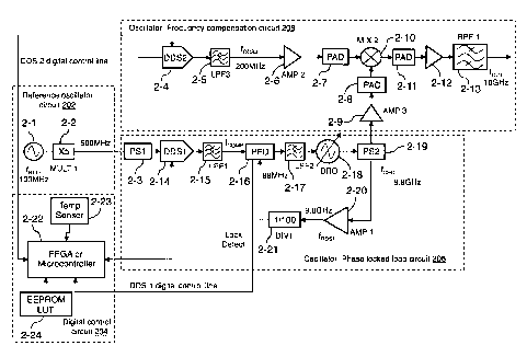
as prior art
with regard to the present invention.
SUMMARY
[0004] In a first aspect, the present disclosure provides a digitally
compensated
phase locked oscillator (DCPLO), comprising: a DCPLO input for receiving a
reference
signal at a known frequency; a DCPLO output for outputting a signal at a
desired
frequency; a phased locked loop (PLL), the phased locked loop comprising: a
phase
frequency detector; an oscillator; a PLL output coupled to the output; a first
direct digital
synthesizer (DDS), the first DDS having an output coupled to the PLL to supply
a DDS
signal to the PLL for adjusting a frequency within the PLL; a temperature
sensor; and a
processor coupled to the first DDS, the phase frequency detector, and the
temperature
sensor, the processor configured to set the frequency of the first DDS
according to a
temperature sensed by the temperature sensor so as to maintain the PLL in a
phase
locked state.
[0005] In some embodiments, the digitally compensated phase locked
oscillator
further comprises: a storage medium coupled to processor, the storage medium
storing a
plurality of first DDS frequencies and associated temperature values; wherein
the
processor is configured to set the frequency of the first DDS by: determining
the
- 1 -
CA 02931341 2016-05-24
WO 2015/074133
PCT/CA2013/050901
temperature sensed by the temperature sensor; identifying a temperature value
stored in
the storage medium closest to the sensed temperature; identifying a first DDS
frequency
stored in the storage medium associated with the identified temperature; and
operating
the first DDS at the identified frequency.
[0006] In various embodiments, the digitally compensated phase locked
oscillator
further comprises a frequency compensation circuit coupled to an output of the
PLL, the
frequency compensation circuit comprising: a second DDS having an input
coupled to the
processor; a mixer, for mixing an output of the second DDS and the output of
the PLL to
produce a mixed signal; and a bandpass filter coupled to an output of the
mixer for
selecting a sideband of the mixed signal. In some embodiments, the processor
is further
configured to set the frequency of the second DDS to produce a mixed signal
having a
desired frequency.
[0007] In various embodiments, the phased locked loop comprises: an
image
rejection mixer coupled between the oscillator and the phase frequency
detector; and a
power splitter (PS) having an input coupled to an output of the image
rejection mixer, a
first PS output coupled to the phase frequency detector and a second PS output
coupled
to the DCPLO output; the first DDS comprises a dual channel DDS having two
outputs in
quadrature for driving an IF port of the image rejection mixer.
[0008] In some embodiments, the digitally compensated phase locked
oscillator
further comprises: a frequency compensation circuit coupled to an output of
the PLL, the
frequency compensation circuit comprising: a second DDS having an input
coupled to the
processor; a mixer, for mixing an output of the second DDS and the output of
the PLL to
produce a mixed signal; and a bandpass filter coupled to an output of the
mixer for
selecting a sideband of the mixed signal. In various embodiments, the
processor is further
configured to set the frequency of the second DDS to produce a mixed signal
having a
desired frequency.
[0009] In some embodiments, the phased locked loop further comprises:
an
image rejection mixer coupled between the oscillator and the phase frequency
detector;
and a power splitter (PS) having an input coupled to an output of the image
rejection
mixer, a first PS output coupled to the phase frequency detector and a second
PS output
coupled to the DCPLO output. In various embodiments, the DCPLO further
comprises a
90 degree hybrid coupler coupled between the output of the first DDS and an IF
port of
the image rejection mixer.
[0010] In another aspect, the present disclosure provides a method of
calibrating
the digitally compensated phase locked oscillator, the method comprising: a.
setting the
- 2 -
CA 02931341 2016-05-24
WO 2015/074133
PCT/CA2013/050901
temperature to a first temperature; b. loading a minimum operating
temperature, a
maximum operating temperature, and an output frequency from the storage
medium; c.
measuring a temperature associated with the DCPLO; d. sweeping the frequency
of the
first DDS across a frequency range; e. recording each frequency of the first
DDS at which
the PLL is locked against the measured temperature; f. after completing the
sweep,
calculating a mid frequency of the first DDS based on each of the recorded
frequencies;
and g. storing the mid frequency and the recorded temperature in a look up
table.
[0011] In some embodiments, the method further comprises: h. setting
the
temperature to a second temperature; and repeating b to g for the second
temperature.
[0012] Other aspects and features of the present disclosure will become
apparent
to those ordinarily skilled in the art upon review of the following
description of specific
embodiments in conjunction with the accompanying figures.
BRIEF DESCRIPTION OF THE DRAWINGS
[0013] Embodiments of the present disclosure will now be described, by way
of
example only, with reference to the attached Figures.
[0014] Figure 1 is a graph illustrating several plots of resonator
magnitude and
phase as a function of frequency for a variety of temperatures;
[0015] Figures 2 to 5 are block diagrams of digitally compensated phase
locked
oscillator circuits in accordance with various embodiments;
[0016] Figure 6 is a flow chart diagram illustrating an example method
of
calibrating a digitally compensated phase locked DRO in accordance with the
present
disclosure; and
[0017] Figure 7 is a flow chart diagram illustrating a method of
setting a frequency
in a digitally compensated phase locked DRO in accordance with the present
disclosure.
DETAILED DESCRIPTION
[0018] For simplicity and clarity of illustration, reference numerals
may be
repeated among the figures to indicate corresponding or analogous elements.
Numerous
details are set forth to provide an understanding of the embodiments described
herein.
The example embodiments may be practiced without these details. In other
instances,
well-known methods, procedures, and components have not been described in
detail to
avoid obscuring the embodiments described. The description is not to be
considered as
limited to the scope of the example embodiments described herein.
- 3 -
CA 02931341 2016-05-24
WO 2015/074133
PCT/CA2013/050901
[0019] Two common applications of radio systems are: RADAR and radio
communications. In case of a RADAR system the information is instantiated on a
transmitted radio frequency pulse by the target whereas in a radio
communication
apparatus information is instantiated by the radio transmission device itself.
In both
RADAR and radio communication systems noise present in the stable local
oscillator
causes decreases in the signal to noise power ratio making the reception
system less
sensitive to the information signal. A point is reached where the noise
present in the
transmission and reception apparatus relative to the information signal power
causes the
signal not to be received. In the case of a radio communication system
increased system
noise results in a failure of the system to accurately transmit and receive
information. In
the case of RADAR increased in system noise result in a reduction in the
target detection
range. It is consequently advantageous for radio communication and RADAR
systems
apparatus to generate very little intrinsic noise in order to maximize the
sensitivity to the
information signal.
[0020] The stable local oscillator present in all radio systems ideally
would
produce a signal just at the required operating frequency. In real stable
local oscillators
the power spectral density of the oscillator is distributed over a range of
frequencies
centered about the desired frequency at which most of the oscillator's power
is located.
Spectral broadening of the stable local oscillator is caused by random time
varying phase
perturbations termed phase noise. Phase noise in the transmitter and receiver
stable
local oscillator results in a reduction in the receiver sensitivity. In RADAR
systems phase
noise in the RADAR transceiver stable local oscillator manifests as an
uncertainty in the
Doppler frequency shift and consequently an uncertainty with respect to the
target
velocity. It is consequently advantageous in both radio communications systems
and
RADAR systems to reduce the phase noise contribution of the stable local
oscillator.
[0021] A free running oscillator forms the basic component of a phase
locked
loop. The phase locked loop enables the phase stability of a free running
oscillator to be
corrected with respect to a stable reference oscillator. The stable reference
oscillator
typically operates at a frequency significantly less than that of the free
running oscillator.
The frequency and phase stability of a free running oscillator is determined
by the
resonator used in the positive feedback path of the oscillator. In order to
sustain
oscillation it is necessary for the positive feedback loop of the free running
oscillator to
exhibit more gain than loss and an overall phase shift around the loop equal
to an integer
multiple of 360 degrees.
- 4 -
CA 02931341 2016-05-24
WO 2015/074133
PCT/CA2013/050901
[0022] It is standard practice to phase lock a free running oscillator
which
operates at the desired system frequency, to a fixed frequency crystal
reference. The
operation of phase locking the free running oscillator maintains the
oscillator at a
frequency determined by a multiple of the crystal reference frequency. As the
temperature of the system changes the phase shift across the oscillator loop
components
will change resulting in a change in the operating impedance of the resonant
element of
the oscillator. If the oscillation frequency moves away from the resonance
frequency of
the resonator as a result of changes in the environmental temperature then the
resonator
insertion loss will increase. If there is a sufficiently large increase in
temperature then the
insertion loss of the resonator will exceed the feedback gain of the
oscillator and the
oscillations will stop.
[0023] The change in resonator insertion loss is illustrated in Figure
1. Figure 1 is
graph illustrating several plots of resonator magnitude and phase as a
function of
frequency for a variety of temperatures. Plots 101, 103, and 106 illustrate
resonator
phase as a function frequency for temperatures negative 40 C, positive 25 C,
and
positive 85 C, respectively. Plots 102, 104, and 105, illustrate the resonator
magnitude as
a function of frequency for temperatures positive 25 C, positive 85 C, and
negative 40 C,
respectively. Each of points 1-1, 1-3 and 1-6 represent the resonator phase at
10GHz.
Each of points 1-2, 1-4 and 1-5 represent the resonator insertion loss at
lOGHz. Point 1-2
represents the lowest insertion loss of the resonator, as the operating
temperature is
increased or decreased the insertion loss increases to that of points 1-4 and
1-5.
[0024] The rate of change in insertion loss of the resonator increases
with
resonator quality factor. In order to minimize the oscillator phase noise a
high quality
factor is required, consequently, in the case of high quality factor low noise
oscillators
there is a tradeoff between the phase noise and operating temperature range.
Some
forms of narrow band oscillators, such as dielectric resonator oscillators,
require precise
frequency centering of the resonator, using a mechanical tuning screw, to
ensure that the
oscillation condition is met over the operating temperature range. Even in the
case of
oscillators that employ such mechanical frequency setting the phase noise of
the
oscillator is degraded at the upper and lower operating temperatures because
the rate of
change of phase as a function of frequency offset from resonance decreases
with
increasing offset from the oscillator resonance frequency. Decreasing the
resonator rate
of change of phase increases the instantaneous frequency excursions in the
oscillator
loop required to compensate for random phase fluctuations in the loop
components,
which in turn leads to higher output phase noise levels from the oscillator.
The change in
- 5 -
CA 02931341 2016-05-24
WO 2015/074133
PCT/CA2013/050901
resonator phase gradient is shown in Figure 1. Point 1-3 is the point of
maximum phase
gradient and consequently lowest phase noise which occurs when the oscillation
frequency and resonator resonance frequency are equal. As the oscillator
temperature
increases or decreases the phase gradient decreases as shown by points 1-1 and
1-6,
the reduction in phase gradient results in an increase in the oscillator phase
noise and
subsequent degradation in system performance.
[0025] As mentioned certain resonators such as dielectric resonators
and cavity
resonator use a mechanical tuning screw for frequency centering. Such
mechanical
tuning screws add complexity in the manufacturing process through the
requirement for a
manual alignment phase. Design reliability is also impacted by the use of such
screws as
very small changes in the screw depth can have significant impact on the
operational
frequency of the oscillator. Not using a tuning screw, however, places
stringent
requirements on the oscillator design to meet a specific oscillation
frequency. Practically,
as the tolerance on the oscillation frequency is decreased the time spent in
test and tune
to correct for component variation introduced during manufacture increases. A
way to
mitigate such problems is to reduce the quality factor of the resonator to
make the design
less sensitive to the resonator mechanical tolerances, however, reduction in
resonator
quality factor results in an increase in oscillator phase noise and as such
reduces the
ultimate system performance achievable.
[0026] Various embodiments disclosed herein avoid the use of a mechanical
adjustment or resonator quality factor reduction and provides a means by which
the
oscillator can be maintained at its lowest phase noise over the operational
temperature
range of the system. Furthermore, the approach reduces the tolerance placed on
the
oscillator center frequency which can reduce and even eliminate the
requirement for post
production tuning. The embodiments described herein are applied primarily to a
phase
locked dielectric resonator oscillators, however, various embodiments
described herein
could equally be applied to optimize the phase noise performance of any
oscillator over
extended temperature range operation whilst reducing the tolerance on the
oscillation
design center frequency to improve manufacturing yield and reduce design test
and tune
time.
[0027] An embodiment of the invention is described in detail with
reference to the
block diagram of Figure 2. Figure 2 represents a general embodiment of the
invention.
The block diagram of Figure 2 consists of four main sub circuits consisting
of: the
reference oscillator circuit 202; the digital control circuit 204; the offset
phase locked loop
206 and the oscillator frequency compensation circuit 208.
- 6 -
CA 02931341 2016-05-24
WO 2015/074133
PCT/CA2013/050901
[0028] The operation of the circuit is described with respect to
application to a
dielectric resonator oscillator, DRO, however, for those skilled in the art
generalization of
the approach to other oscillator technologies will be obvious based on the
present
disclosure. It is assumed that the DRO, 2-18, has been designed for operation
at 10GHz.
The DRO is also assumed to have no mechanical frequency adjustment screw. The
frequency of DDS 1, 2-14, is initially set to 95MHz, since the actual
operating frequency
of the DRO is 9.8GHz the phase frequency detector, 2-16, lock detect circuit
registers a
logic level low indicating an unlocked state. The FPGA , 2-22, of the digital
control circuit
on receiving the unlock status, records the system operating temperature using
temperature sensor, 2-23, and initiates a frequency sweep of DDS 1, 2-14, from
95MHz
to 105MHz in steps of 100KHz. During the frequency sweep the lock detect
signal will
toggle from low to high and then back to low signifying a range of frequencies
over which
the phase locked loop is locked. The locked frequency settings and operating
temperature are stored in the EEPROM, 2-24, and on completion of the sweep the
central
value of the locked range is calculated and programmed into DDS1, 2-14, by the
digital
control circuit FPGA, 2-22.
[0029] First operation of the embodiment described herein consequently
establishes phase lock of the DRO based on a blind frequency search. The DDS1
output
frequency is known because of the mathematical relationship it has to the
reference
oscillator frequency. In order for the phase locked loop to be locked the DRO
frequency
must be exactly equal to DDS 1 frequency multiplied by the value of the fixed
frequency
divider DIV 1, 2-21, present in the phase locked loop feedback path,
consequently, under
locked condition the DRO frequency is known. Based on the block diagram of
Figure 2
the DRO frequency would be determined to be 9.8GHz. 00S2, 2-4, is then
programmed
to output 200MHz, which when mixed with the DRO 9.8GHz signal in mixer MIX 2,
2-10,
establishes the required 10GHz signal as the upper sideband. The band pass
filter, BPF
1, 2-13, is selected to reject the lower sideband leaving the desired 10GHz
output signal.
[0030] The operational temperature of the system is monitored by the
temperature sensor 2-23. In production test and calibration of the unit in
accordance with
various embodiments described herein would be placed in a temperature chamber
and
cycled over the operational temperature range. Every 20 C the lock range scan
is
conducted and the center frequency of the lock range stored in the look up
table located
in the EEPROM, 2-24, along with the associated temperature. Once this
calibration cycle
has been completed the frequency of DDS 1,2-14, can be adjusted in order to
maintain
the DRO, 2-18, in the center of the lock range irrespective of the operating
temperature. It
- 7 -
CA 02931341 2016-05-24
WO 2015/074133
PCT/CA2013/050901
should be noted that the center of the lock range also represents the
resonance
frequency of the dielectric resonator present in the DRO, 2-18, and as such
the lowest
phase noise operating point for the DRO. Various embodiments disclosed herein
ensure
that the DRO, 2-18, is always operating in its lowest phase noise mode.
[0031] In the case that the DRO frequency is say 10.2 GHz the 200MHz DDS 2,
2-4, frequency setting is still used, however, the lower sideband is now
selected from
mixer MIX 2, 2-10. Various embodiments thus enable the arbitrary DRO frequency
associated with the lowest phase noise condition to be corrected to the
required output
frequency by mixing with the adjustable output frequency of 00S2. Low
frequency
operation of DDS 2 ensures that the DDS phase noise does not limit the phase
noise of
the output signal of the system. Use of higher frequency DDS for DDS 2 can be
employed
if increased rejection of the unwanted sidebands from MIX 2 is required.
[0032] A second implementation of the embodiments disclosed herein is
presented in Figure 3. The digitally compensated phase locked oscillator
circuit of Figure
3 includes a reference oscillator circuit 302, a digital control circuit 304,
and an offset
phase locked loop circuit 306. In the implementation of Figure 3 the
comparison
frequency, fcomp, is fixed at 100MHz. An offset signal is mixed with the DRO
signal to
establish the correct conditions for phase lock of the loop. The offset signal
is generated
by 0051, 3-11, which in this embodiment is a dual channel DDS capable of
providing two
outputs in quadrature necessary to drive the IF port of the image rejection
mixer 3-7. The
basic operation of the embodiments remains the same as in the case of the
block
diagram of Figure 2. The operational temperature is recorded and the frequency
of DDS 1
changed whilst monitoring the lock detection signal. Following the frequency
sweep DDS
1 is programmed with the frequency at the center of the lock range. Under
locked
operation the signal output from power splitter PS 3, 3-8, has to be the
comparison
frequency multiplied by the divide ratio of DIV 2, 3-9. Consequently, in the
embodiment of
Figure 3, an additional mixer is not required to correct to DRO phase locked
frequency.
The extracted frequency is equal to the comparison frequency multiplied by the
division
setting in DIV 2. The use of an offset phase locked loop 306 also is
advantageous in that
it reduces the phase noise and spurious contribution of the DDS1 to the source
output
[0033] Figure 4 illustrates another embodiment of a digitally
compensated phase
locked oscillator, which comprises a reference oscillator circuit 402, a
digital control circuit
404, an offset phase locked loop circuit 406, and an oscillator frequency
compensation
circuit 408. In the alternate embodiment of Figure 4 the offset phase locked
loop 406 is
used as in Figure 3 but the frequency compensation path is re-introduced. The
approach
- 8 -
CA 02931341 2016-05-24
WO 2015/074133
PCT/CA2013/050901
is included as it provides additional flexibility in terms of frequency
planning and spurious
reduction. Once again the underlying principle of operation remains the same
the offset
loop is used to establish phase lock between the reference and the DRO at the
optimal
operating point of the DRO with respect to its phase noise performance and the
compensation path corrects for the variability in the DRO operating frequency.
[0034] Figure 5 illustrates another embodiment of a digitally
compensated phase
locked oscillator, which comprises a reference oscillator circuit 502, a
digital control circuit
504, an offset phase locked loop circuit 506, and an oscillator frequency
compensation
circuit 508. In the implementation of Figure 5 a hybrid power splitter has
been used to
create the quadrature signals required by the image rejection mixer, 5-18,
this approach
allows the use of a single channel DDS 1, 5-22, and could be implemented as a
simplification to the embodiment of Figure 4.
[0035] In various embodiments disclosed herein the characteristics of
the
oscillator are determined over the operating temperature of the circuit as
part of the initial
circuit calibration. Figure 6 illustrates a flow chart of an example method of
calibrating a
digitally compensated phase locked oscillator in accordance with the present
disclosure.
The method may be carried out by software executed by, for example, one or
more
processors. The processor can be, for example, a FPGA or a microcontroller.
Programming of the processor for carrying out such a method is within the
scope of a
person of ordinary skill in the art given the present description. The method
may contain
additional or fewer processes than shown and/or described, and may be
performed in a
different order. In some embodiments, computer-readable code executable by at
least
one processor to perform the method may be stored in a computer-readable
medium,
such as a non-transitory computer-readable medium.
[0036] At 6-1, calibration is initiated.
[0037] At 6-2, the processor loads the minimum and maximum operating
temperatures an output frequency from a memory device. The memory device can
be, for
example, an Electrically Erasable Programmable Read-Only Memory (EEPROM) as
illustrated in figures 2 to 5. In various embodiments, the processor can be,
for example, a
field-programmable gate array (FPGA) or a microcontroller.
[0038] At 6-3, the temperature is measured by a temperature sensor.
[0039] At 6-4, a processor determines whether the temperature is within
a
threshold distance from the minimum operating temperature. In some
embodiments, the
threshold is 5 C. If it is determined that the temperature is not within a
threshold distance
of the minimum operating temperature, then the temperature is measured again
at 6-3.
- 9 -
CA 02931341 2016-05-24
WO 2015/074133
PCT/CA2013/050901
On the other hand, if it is determined that the measured temperature is within
a threshold
distance of the minimum operating temperature, then the method proceeds to 6-
5.
[0040] At 6-5, the processor sets the frequency of DDS 1 to the minimum
sweep
frequency.
[0041] At 6-6, the lock status of the PLL is checked.
[0042] At 6-7, it is determined whether the PLL is in a locked state.
If the PLL is in
a locked state, then the method proceeds to 6-8 followed by 6-9. If the PLL is
not in a
locked state, the method proceeds to 6-9 and 6-8 is omitted.
[0043] At 6-8, the DDS 1 frequency and the measured temperature are
stored in
the memory device. In the present disclosure, the terms "stored" and
"recorded", when
used in reference to a memory device, are used interchangeably.
[0044] At 6-9, it is determined whether the current DDS1 frequency is
equal to the
maximum sweep frequency. If the DDS 1 frequency is not at the maximum sweep
frequency, then 6-10 is executed. Otherwise, the method proceeds to 6-11.
[0045] At 6-10, the DDS 1 frequency is incremented. For example, in some
embodiments it is incremented by 100kHz. After 6-10 has been executed, the
method
proceeds to 6-3.
[0046] At 6-11, a mid-frequency of DDS 1 is calculated based on the DDS
1
frequencies stored in memory at 6-8.
[0047] At 6-12, a frequency value for DDS 2 is calculated based on the
output
frequency and the DDS 1 value.
[0048] At 6-13, the measured temperature and the mid-frequency of DDS 1
is
stored in memory. In various embodiments disclosed herein, these values are
stored in a
lookup table.
[0049] At 6-14, DDS 1 is reset to the minimum sweep frequency value.
[0050] At 6-15, the processor determines whether the temperature is
within a
threshold distance from the maximum operating temperature. In some
embodiments, the
threshold is 5 C. If it is determined that the temperature is not within a
threshold distance
of the maximum operating temperature, then the temperature is measured again
at 6-16.
On the other hand, if it is determined that the measured temperature is within
a threshold
distance of the maximum operating temperature, then the method proceeds to 6-
17.
[0051] At 6-16, the minimum operating temperature is incremented. In
some
embodiments, the minimum operating temperature is increased by 20 C.
[0052] At 6-17, the calibration complete flag is set.
[0053] At 6-18, the calibration is completed.
- 10-
CA 02931341 2016-05-24
WO 2015/074133
PCT/CA2013/050901
[0054] After calibration of the unit, the frequency setting method of
Figure 7
operates to maintain optimal operation of the source over the calibration
temperature
range. Figure 7 is a flow chart illustrating an example of a method of
operating a system
including a digitally compensated phase locked oscillator such as those
illustrated in
Figures 2 to 5 of the present disclosure. The method may be carried out by
software
executed by, for example, a processor. The processor can be, for example, a
FPGA or a
microcontroller. Programming of the processor for carrying out such a method
is within
the scope of a person of ordinary skill in the art given the present
description. The method
may contain additional or fewer processes than shown and/or described, and may
be
performed in a different order. In some embodiments, computer-readable code
executable by at least one processor to perform the method may be stored in a
computer-
readable medium, such as a non-transitory computer-readable medium.
[0055] At 7-1, the temperature sensor is read.
[0056] At 7-2, the temperature sensor reading is stored in the
operating
temperature variable.
[0057] At 7-3, the processor identifies the temperature value stored in
the lookup
table that is closest to the temperature read by the temperature sensor and
stored in the
operating temperature variable. In some embodiments, this is achieved by
subtracting the
operating temperature variable from each of the values stored in the lookup
table and
storing the results in a new table. Then the value having the smallest
magnitude in the
new table is selected.
[0058] At 7-4, the DDS 1 and DDS 2 frequency setting values associated
with the
identified temperature are loaded from memory.
[0059] At 7-5, as the system is operated the temperature is measured.
[0060] At 7-6, the processor determines whether the measured temperature is
within a threshold value of the stored operating temperature variable value.
In some
embodiments, the threshold corresponds to 5 C. If the measured temperature is
within
the threshold value the stored operating temperature, then the system
continues to
operate with the current DDS 1 and DDS 2 frequency settings and the
temperature is
measured again at 7-5. On the other hand, if the temperature measured at 7-5
is not
within the threshold, then the method returns to 7-2.
[0061] In the preceding description, for purposes of explanation,
numerous details
are set forth in order to provide a thorough understanding of the embodiments.
However,
it will be apparent to one skilled in the art that these specific details are
not required. In
other instances, well-known electrical structures and circuits are shown in
block diagram
- 11 -
CA 02931341 2016-05-24
WO 2015/074133
PCT/CA2013/050901
form in order not to obscure the understanding. For example, specific details
are not
provided as to whether the embodiments described herein are implemented as a
software
routine, hardware circuit, firmware, or a combination thereof.
[0062] Embodiments of the disclosure can be represented as a computer
program
product stored in a machine-readable medium (also referred to as a computer-
readable
medium, a processor-readable medium, or a computer usable medium having a
computer-readable program code embodied therein). The machine-readable medium
can
be any suitable tangible, non-transitory medium, including magnetic, optical,
or electrical
storage medium including a diskette, compact disk read only memory (CD-ROM),
memory device (volatile or non-volatile), or similar storage mechanism. The
machine-
readable medium can contain various sets of instructions, code sequences,
configuration
information, or other data, which, when executed, cause a processor to perform
steps in a
method according to an embodiment of the disclosure. Those of ordinary skill
in the art
will appreciate that other instructions and operations necessary to implement
the
described implementations can also be stored on the machine-readable medium.
The
instructions stored on the machine-readable medium can be executed by a
processor or
other suitable processing device, and can interface with circuitry to perform
the described
tasks.
[0063] The above-described embodiments are intended to be examples
only.
Alterations, modifications and variations can be effected to the particular
embodiments by
those of skill in the art without departing from the scope, which is defined
solely by the
claims appended hereto.
- 12-