Note: Descriptions are shown in the official language in which they were submitted.
CA 02931471 2016-05-24
WO 2015/077782 PCT/US2014/067440
1
WIRELESS CHARGING COIL
SPECIFICATION
BACKGROUND
FIELD OF THE DISCLOSURE
The present disclosure relates to a wireless charging coil and methods for
manufacturing thereof. More specifically, the present disclosure relates to a
bifilar parallel
wound, series connected wireless charging coil.
RELATED ART
Wireless power transfer is the transfer of electrical power from a base
station
(transferring power) to a mobile device (consuming power) through
electromagnetic induction
(inductive power) and/or resonant frequency method. Wireless power transfer is
becoming
increasingly popular in mobile devices, and particularly in smartphones. A
popular standard
for inductive charging technology is the Qi interface standard developed by
the Wireless
Power Consortium, which has several protocols to allow the wireless transfer
of electrical
power between electronic devices. Other standards may make use of
electromagnetic
induction or resonant frequency to wirelessly charge devices. A mobile device
(or any other
electronic device) must meet certain requirements and performance standards in
order to be Qi
compliant.
Consumers generally want their mobile devices to be small and thin but also
powerful
and efficient, which are often counteracting goals. More specifically,
charging coils must vary
the material thickness to lower resistance and increase efficiency. Further,
maximizing these
goals can lead to performance and manufacturing limitations.
What would be desirable, but has not yet been developed, is a thinner and more
efficient wireless charging coil for wireless power transfer between
electronic devices.
CA 02931471 2016-05-24
WO 2015/077782 PCT/US2014/067440
2
SUMMARY
The present disclosure relates to wireless charging coils and methods for
making
thereof. More specifically, the present disclosure relates to a planar bifilar
parallel-wound,
series connected wireless charging coil. The coil has a thinner thickness
(e.g., low profile), an
increased density (e.g., high fill factor), and higher efficiency (e.g., lower
resistance) than
conventional wireless charging coils.
CA 02931471 2016-05-24
WO 2015/077782 PCT/US2014/067440
3
BRIEF DESCRIPTION OF THE DRAWINGS
The foregoing features of the disclosure will be apparent from the following
Detailed
Description, taken in connection with the accompanying drawings, in which:
FIG. 1 is a diagram showing processing steps for manufacturing a wireless
charging
coil;
FIG. 2 is a schematic view of a first stamped coil with tie bars;
FIG. 3 is a schematic view of a second stamped coil with tie bars;
FIG. 4 is a schematic view of an assembled coil after the tie bars of the
first and
second stamped coils have been removed;
FIG. 5 is a schematic view of the assembled wireless charging coil with
jumpers
attached;
FIG. 6 is a close up view of portion A of FIG. 5;
FIG. 7 is a schematic view of an electrical component assembly including a
wireless
charging coil and NFC antenna;
FIG. 8 is a schematic view of an assembled wireless charging coil with planar
bifilar
coils;
FIG. 9 is a cross-sectional view of a portion of the wireless charging coil of
FIG. 8;
FIG. 10 is a schematic view of an assembled wireless charging coil with
stacked
bifilar coils;
FIG. 11 is a cross-sectional view of a portion of the wireless charging coil
of FIG. 10;
FIG. 12 is a perspective view of an electrical component assembly;
FIG. 13 is an exploded view of the electrical component assembly of FIG. 12
FIG. 14 is a perspective view of a resonant coil;
FIG. 15 is a perspective view of a resonant coil assembly;
FIG. 16 is a perspective view of a folded stamped resonant coil;
FIG. 17 is a perspective view of the coil of FIG. 16 partially opened;
FIG. 18 is a perspective view of the coil of FIG. 16 fully opened;
FIG. 19 is an exploded view of a low profile electrical component assembly;
and
FIG. 20 is a perspective view of the filler material of FIG. 19;
FIG. 21 is a diagram showing processing steps for manufacturing a wireless
charging
coil with adhesive;
CA 02931471 2016-05-24
WO 2015/077782 PCT/US2014/067440
4
FIG. 22 is a partial cross-sectional view of a first stamped coil when applied
to a first
laminate;
FIG. 23 is a partial cross-sectional view of an assembled coil positioned
between a
first and second laminate;
FIG. 24 is partial cross-sectional view of an assembled coil;
FIG. 25 is a partial top view of the assembled coil of FIG. 24; and
FIG. 26 is a top view of an assembled coil of the present disclosure.
CA 02931471 2016-05-24
WO 2015/077782 PCT/US2014/067440
DETAILED DESCRIPTION
The present disclosure relates to a wireless charging coil and methods of
making same.
As discussed in more detail below in connection with FIGS. 1 ¨ 7, the stamped
metal wireless
charging coil comprises a series of parallel traces connected in a bifilar
fashion. In other
5 words, the wireless charging coil includes first and second coils that
are parallel, closely
spaced, and connected in series such that the first and second coils have
parallel currents. The
first and second coils could be stacked or planar and connected in series
and/or parallel to
meet performance requirements (e.g., electrical requirements, power
requirements, etc.). The
wireless charging coil could be used in any battery powered device,
particularly in mobile
devices (e.g., smartphones, tablets, watches, etc.). The wireless charging
coil can be made to
be Qi compliant, but could be adjusted to comply with any wireless transfer
protocol. A
wireless charging coil with a greater amount of conductive material, such as
copper, can be
positioned within a given space by varying (e.g., increasing) the thickness of
the coil, which
increases energy availability. Compared with other wireless charging coils,
the wireless
charging coils described herein exhibit an increased magnetic coupling
effectiveness (e.g.,
magnetic field strength) and thereby transmit energy at a higher efficiency.
FIG. 1 is a diagram showing processing steps 10 for manufacturing a wireless
charging coil of the present disclosure. In step 12, a metal sheet is stamped
to form a first coil
with tie bars. The metal sheet could be any of a variety of materials suitable
for wireless
power transfer (e.g., copper, copper alloy, aluminum, aluminum alloy, etc.).
In step 14, a
metal sheet (e.g., the same metal sheet or a different metal sheet) is stamped
to form a second
coil with tie bars. In step 16, the first coil is stamped to remove the tie
bars. In step 18, the
second coil is stamped to remove the tie bars. In step 20, the first and
second coils are
assembled together. In step 22, the assembled coil is applied to a ferrite
substrate. In step 24,
jumpers (e.g., leads) are attached to electrically connect the first and
second coils in series
(e.g., an inside end of the first coil is electrically connected to the
outside end of the second
coil via a jumper).
The steps described above could be interchanged, consolidated, or omitted
completely.
For example, the coils could be stamped without first forming tie bars, and/or
the first and
second coils could be applied directly to the ferrite (without being assembled
first), etc.
6
Additionally, the coil could be photo-chemically etched or machined instead of
stamped, or
made by any other suitable manufacturing process.
FIG. 2 is a view of a first stamped coil 30 with tie bars. The first coil 30
can be a
generally rectangular planar spiral trace 31, although the trace 31 could form
any suitable
shape (e.g., circular planar spiral). The dimensions of the coil 30 could vary
depending on the
application of the coil 30 (e.g., as used in mobile devices, wearable devices,
cars, etc.). The
coil 30 could be of any suitable thickness, such as between 0.003 in. and
0.020 in., etc., but
could be thicker for higher powered applications. The coil 30 could be of any
suitable overall
dimensions, such as between 0.25 in. and 4 in. in width and/or between 0.25
in. and 4 in. in
height. The trace 31 could also be of any suitable dimensions. For example,
the trace 31
could be between 0.005 in. and 0.250 in. in width. The dimensions could vary
depending on
physical and performance requirements of the mobile device (e.g., required
frequency). The
coil 30 could be made of any suitable material for wireless power transfer,
such as, for
example, copper, copper alloy, aluminum, aluminum alloy, tempered copper alloy
(e.g.,
C110), etc.
The trace 31 of the coil 30 revolves around a center any number of times
(e.g., 5, 10,
etc.), such as to comply with any inductive or resonant power requirements.
The trace 31
spirals to form an inside portion 32 at the center of the coil 30. As a
result, the coil 30 has an
inside end 34 and an outside end 36. The spaces 38 between the trace 31 are
configured to be
wide enough (e.g., 0.0285 in.) to accommodate the second stamped coil
(described in more
detail below). Tie bars 40 can be positioned at a plurality of locations
throughout these spaces
38 to maintain the general shape of the coil 30 (e.g., prevent unwinding or
deformation of the
shape), such as during transportation of the coil 30 between locations or
between stations. The
outside end 36 could extend out at an angle, such as a generally ninety degree
angle. The
inside end 34 and outside end 36 can be disposed towards the same side of the
coil 30, but
could be at any of a variety of locations in the coil 30.
FIG. 3 is a view of a second stamped coil 50 with tie bars. The second coil 50
shares
most of the same features and characteristics of the first coil shown in FIG.
2. The second
coil 50 can be a generally rectangular planar spiral trace 51, although the
trace 51 could form
any suitable shape (e.g., circular planar spiral). The dimensions of the coil
50 could vary
depending on the application of the coil 50 (e.g., as used in mobile devices,
wearable devices,
CA 2931471 2019-11-21
=
7
cars, etc.). The coil 50 could be of any suitable thickness, such as between
0.003 in. and 0.020
in., etc., but could be thicker for higher powered applications. The coil 50
could be of any
suitable overall dimensions, such as between 0.25 in. and 4 in. in width
and/or between 0.25
in. and 4 in. in height. The trace 51 could also be of any suitable
dimensions. For example
the trace 51 could be between 0.005 in. and 0.250 in. in width. The dimensions
could vary
depending on physical and performance requirements of the mobile device (e.g.,
required
frequency). The coil 50 could be made of any suitable material for wireless
power transfer,
such as, for example, copper, copper alloy, aluminum, aluminum alloy, tempered
copper alloy
(e.g., C110), etc.
The trace 51 of the coil 50 revolves around a center any number of times
(e.g., 5, 10,
etc.), such as to comply with any inductive or resonant power requirements.
The trace 51
spirals to form an inside portion 52 at the center of the coil 50. As a
result, the coil 50 has an
inside end 54 and an outside end 56. The spaces 58 between the trace 51 are
configured to be
wide enough (e.g., 0.0285 in.) to accommodate the first stamped coil 30
(described above).
Tie bars 60 can be positioned at a plurality of locations throughout these
spaces 58 to maintain
the general shape of the coil 50 (e.g., prevent unwinding or deformation of
the shape), such as
during transportation of the coil 50 between locations or between stations.
The outside end 56
does not extend out as with the first coil 30 (but could). The inside end 54
and outside end 56
can be disposed towards the same side of the coil 50, but could be at any of a
variety of
.. locations in the coil 50.
FIG. 4 is a view of an assembled coil 170 after the tie bars of the first and
second
stamped coils 130, 150 have been removed. As shown, the first and second coils
130, 150 fit
into each other. More specifically, the first coil 130 fits into the space
formed between the
trace 151 of the second coil 150, and conversely, the second coil 150 fits
into the space formed
between the trace 131 of the first coil 130. However, when assembled, there
are small gaps
between the trace 131 of the first coil 130 and the trace 151 of the second
coil 150 (e.g., 0.003
in., 0.004 in., etc.), as discussed below in more detail. As a result,
together the first and
second coils 130, 150 together form a parallel planar spiral. Also shown, the
inside end 134 of
the first coil 130 is adjacent to the inside end 154 of the second coil 150,
and the outside end
136 of the first coil 130 is adjacent to the outside end 156 of the second
coil 150. However,
the ends could be any relative distance from one another. This stamping method
could have
CA 2931471 2019-11-21
CA 02931471 2016-05-24
WO 2015/077782 PCT/US2014/067440
8
an average space width variation of at least approximately 0.003 in. for the
assembled coil
170. The maximum and minimum variance are dependent on the assembled coil 170
dimensions (e.2., overall height and width).
The tight tolerances and rectangular cross-sectional shape of the traces 130,
131 could
result in a fill ratio (e.g., 85%) greater than current industry coils (e.g.,
65%), such as wound
coils, etched coils, etc. For example, the rectangular cross-sectional shape
achieved from
stamping (see FIG. 9 below) provides a potentially greater fill ratio than the
circular cross-
sectional shape of a round wire (e.g., round copper wire). More specifically,
a 0.010 in.
diameter insulated round wire (0.009 diameter in. wire with 0.0005 in.
insulation) could
provide a 65% fill ratio, compared to a stamped coil with a rectangular cross
section having a
0.006 thickness and 0.003 spacing gap. Further, the wireless charging coil 170
can operate
under higher ambient temperatures than other current industry wires (e.g.,
Litz wire), and is
not susceptible to degradation by vibration, shock, or heat. This is partly
because the wireless
charging coil 170 is made of a single-monolithic conductor (e.g., not a multi-
strand wire).
This can be compared to the individual strands of a Litz wire, which has
insulation material
separating each of the individual wire strands which cannot withstand higher
temperatures.
FIG. 5 is a view of the assembled wireless charging coil 270 with jumpers
attached.
Although not shown, a jumper could be attached to the first outside end 236.
As shown, the
inside end 234 of the first coil 230 is electrically connected to the outside
end 256 of the
second coil 250 by a first jumper 274. These ends 234, 256 are relatively
proximate to one
another, and disposed on the same side of the coil 270 to allow for a short
jumper 274. A
second jumper 276 is then used to electrically connect the inside end 254 of
the second coil
with the mobile device circuitry. The outside end 236 and inside end 254 are
relatively
proximate and disposed towards the same side of the coil 270, to provide for a
short jumper
276 and for ease of electrical wiring with the electronic device. The result
is a pair of parallel,
closely spaced coils 230, 250 connected in series such that the first and
second traces 230, 250
have parallel currents (e.g., the currents of each trace are in the same
clockwise or counter-
clockwise direction).
When fully assembled with the other components of the electronic device, the
inside
portion 272 of the assembled coil 270 is insulated (e.g., by plastic and glue)
to ensure proper
performance. The assembled wireless charging coil 270 can have any number of
windings,
CA 02931471 2016-05-24
WO 2015/077782 PCT/US2014/067440
9
depending upon electrical requirements. The wireless charging coil 270 could
be used in any
battery powered device, such as smartphones. The assembled coil 270 could be
of any
suitable overall dimensions (e.g., L142 in. width and L457 in. height, etc.).
The coil length
could be of any suitable length (e.g., 48.459 in.).
FIG. 6 is a close up view of portion A of FIG. 5. As shown, there are very
small gaps
278 (e.g., voids) between the trace 231 of the first coil 230 and the trace
251 of the second coil
250 (e.g., 0.003 in., 0.004 in., etc.), although there could be increased gaps
280 at the corners
to account for the bends in the traces 231, 251 (e.g., such that the gap
increase alternates).
These tight tolerances could result in a fill ratio greater than current
industry methods.
The assembled wireless charging coil 270 could provide direct current (DC)
resistance
(ohms), alternating current (AC) resistance, and/or AC/DC resistance ratios at
a number of
different values depending on the dimensions of the charging coil 270 and
material(s) used in
construction of the charging coil. The values could be adjusted to achieve
high AC/DC ratios
to meet induction standards. The coil dimensions could be varied to achieve
varying
resistance depending on the performance characteristics required. For example,
for a
resistance of 0.232 ohms using C110 alloy, the traces 230, 250 could have a
cross section of
0.0001234 in.2 (e.g., 0.005 in. thickness and 0.0246 in. width, or 0.004 in.
thickness and
0.0308 in. width, etc.), and for a resistance of 0.300 ohms using C110 alloy,
the traces 230,
250 could have a cross section of 0.0000953 in.2 (e.g., 0.005 in. thickness
and 0.019 in. width,
or 0.004 in. thickness and 0.0238 in. width, etc.). The stamped wireless
charging coil 270 can
achieve a high trace thickness and/or high overall aspect ratio compared to
other current
industry methods (e.g., printed circuit board (PCB) etched coils).
FIG. 7 is a view of an electrical component assembly 390 including a wireless
charging coil 370. More specifically, the wireless charging coil 370 is
attached to ferrite
substrate 392 and in conjunction with a near field communication (NFC) antenna
394 having
contact paddles. The wireless charging coil 370 and NFC antenna 394 could have
contact
pads (e.g., gold) to connect the wireless charging coil 370 and NFC antenna
394 to the
circuitry of the mobile device. The assembly comprises a first jumper 374, a
second jumper
376, and a third jumper 377 connecting the various ends of the coil 370, as
explained above in
more detail. There could be a film (e.g., clear plastic) over the wireless
charging coil 370 and
NFC antenna 394, with the jumpers 374, 376, 377 on top of the film and only
going through
CA 02931471 2016-05-24
WO 2015/077782 PCT/US2014/067440
the film at the points of connection. This prevents accidentally shorting any
of the electrical
connections of the coil 370. Alternatively, the jumpers 374, 376, 377 could be
insulated so
that a film is not needed. To minimize space, the wireless charging coil 370
is within the NFC
antenna 394 with jumpers 376, 377 that extend to the outside of the NFC
antenna 394.
5 However, the wireless charging coil 370 and jumpers 376, 377 could be
placed at any location
relative to the NFC antenna 394.
The total thickness of the assembly could vary depending on various potential
needs
and requirements. For example, the jumpers could be 0.05-0.08 mm thick, the
film could be
0.03 mm thick, the NFC antenna 394 and coil 370 could be 0.08 mm thick, and
the ferrite 392
10 .. could be 0.2 mm thick for a total wireless charging coil thickness of
approximately 0.36 mm.
FIG. 8 is a schematic view of an assembled wireless charging coil 470 with
planar
bifilar coils. As discussed above, the wireless charging coil 470 includes a
first coil 430 (e.g.,
trace) and a second coil 450 (e.g., trace). The assembled coil 470 is
manufactured and
operates in the manner discussed above with respect to FIGS. 1-7. The first
coil 430 and the
second coil 450 can have any desired thickness, such as to meet different
power requirements.
The first coil 430 and second coil 450 could be connected in series or
parallel.
The width of the first and/or second coil 430, 450 could vary along the length
of the
coil to optimize performance of the assembled wireless charging coil 470.
Similarly, the
thickness of the first and second coils 430, 450 could change over the length
of the coil. For
example, the width (and/or thickness) of the first coil 430 could gradually
increase (or narrow)
from a first end 434 towards a middle of the coil 430, and the width (and/or
thickness) could
likewise gradually narrow (or increase) from the middle to the second end 436
of the coil 430
(e.g., a spiral coil of wide-narrow-wide), thereby varying the cross-sectional
area throughout.
Any variation of width (e.g., cross-section) or thickness could be used,
and/or these
dimensions could be maintained constant over portions of the coil, according
to desired
performance characteristics.
Additionally (or alternatively), the spaces between the windings of the coil
could be
varied to optimize performance of the wireless charging coil 470. For example,
the gap width
between the traces could be wider towards the outside of the first coil 430
and narrower
towards the inside of the first coil 430 (or the opposite). Similarly, the
distance between the
first coil 430 and second coil 450 in the assembled coil 470 could also be
varied to optimize
CA 02931471 2016-05-24
WO 2015/077782 PCT/US2014/067440
11
performance. Further, the geometry of the edges of the coil could be varied
(e.g., scalloped,
castellated, etc.), such as to reduce eddy currents.
FIG. 9 is a cross-sectional view of a portion of the wireless charging coil of
FIG. 8.
The first coil 430 comprises sections 414-424 and the second coil 450
comprises sections 402-
412. As shown, the cross-section of the first coil 430 becomes gradually wider
and then
narrower from a first end to a second end of the first coil 430. As a result,
sections 414 and
424 are the narrowest (e.g., 0.025 in.), followed by sections 404 and 422
(e.g., 0.030 in.), and
sections 418 and 420 are the widest (e.g., 0.035 in.). In the same way, the
cross-section of the
second coil 450 becomes gradually wider and then narrower from a first end to
a second end
.. of the second coil 450. As a result, sections 402 and 412 are the
narrowest, and sections 406
and 408 are the widest. Changes in the dimensions of the cross section of the
antenna can
likewise be varied in other manners.
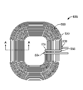
FIG. 10 is a schematic view of an assembled wireless charging coil 570 with
stacked
bifilar coils. As discussed above, the wireless charging coil 570 includes a
first coil 530 and a
.. second coil 550. The assembled coil 570 is manufactured and operates in the
manner
discussed above with respect to FIGS. 1-7, as well as that discussed in FIGS.
8-9, except that
the first and second coils 530, 550 are stacked instead of planar. The first
coil 530 includes a
first end 534 and a second end 536, and the second coil 550 includes a first
end 554 and a
second end 556. Further, varying the skew or offset (e.2., stacking distance)
of the first coil
.. 530 relative to the second coil 550 can affect the performance of the
wireless charging coil
570. The first coil 530 and second coil 550 could be connected in series or
parallel.
FIG. 11 is a cross-sectional view of a portion of the wireless charging coil
of FIG. 10.
This coil 570 is similar to that of FIGS. 8-9, including a first coil 530 with
sections 514-524
and a second coil 550 with sections 502-512, except that the first and second
coils 530, 550
.. are stacked instead of planar.
FIGS. 12-13 are views showing an electrical component assembly 690. More
specifically, FIG. 12 is a perspective view of an electrical component
assembly 690. The
electrical component assembly 690 comprises a ferrite shield 692, a pressure
sensitive
adhesive (PSA) layer 602 positioned on the ferrite shield 692, an assembled
coil 670 (e.g.,
bifilar coil) positioned therebetween, and jumpers 674, 676 positioned on the
PSA layer 602.
=
12
FIG. 13 is an exploded view of the electrical component assembly 690 of FIG.
12.
The bifilar coil 670 includes a first coil 630 having an inside end 634 and an
outside end 636
interconnected with a second coil 650 having an inside end 654 and an outside
end 656. The
inside and outside ends are on the same side of the assembled coil 670 for
ease of use and
assembly (e.g., minimize the distance to electrically connect the ends).
Ferrite shield 692 includes a first hole 696 and a second hole 698 positioned
to
correlate with the placement of the inside end 634 of the first coil 630 and
the inside end 654
of the second coil 650 (e.g., when the coil 670 is placed onto the ferrite
shield 692. Although
holes 696, 698 are shown as circular, any shape and size openings could be
used (e.g., one
rectangular opening, etc.). These holes 696, 698 facilitate assembly and
welding of the
electrical component assembly 690.
PSA layer 602 and ferrite shield 692 are similarly sized to one another, and
although
shown as rectangular, both could be of any shape (e.g., circular). PSA layer
secures the
relative placement of the assembled coil 670 to the ferrite shield 692. PSA
layer 602 could
have adhesive on one or both sides, and could include a polyethylene
terephthalate (PET) film
area 604 free of adhesive on one or both sides. PET film area 604 facilitates
assembly and
welding of the electrical component assembly 690
PSA layer 602 includes a first hole 606 and a second hole 608 in the PET film
area 604
which correlate in position with the placement of the inside end 634 of the
first coil 630 and
the inside end 654 of the second coil 650 (as well as the first hole 696 and
second hole 698 of
the ferrite substrate 692). Although holes 606, 608 are shown as circular, any
shape and size
openings could be used (e.g., one rectangular opening). Holes 606, 608 provide
access
through the PSA layer 602 to electrically connect jumpers 674, 676 with the
inside ends 634,
654 of the assembled coil 670. The PET film area 604 facilitates attachment of
the jumpers
674, 676 to the assembly 690.
FIG. 14 is a perspective view of a resonant coil 730. Resonant coil 730 could
be a
generally rectangular planar spiral trace 731, although the trace 731 could
form any suitable
shape. The resonant coil 730 includes an inside end 734 and an outside end
736. The trace
731 is stamped on a strip or sheet of metal (e.g., copper, aluminum, etc.).
The dimensions of
the coil 730 could vary depending on the application of the coil 730. The coil
730 could be of
CA 2931471 2019-11-21
CA 02931471 2016-05-24
WO 2015/077782 PCT/US2014/067440
13
any suitable dimensions. The dimensions could vary depending on physical and
performance
requirements. The coil 730 could be made of any suitable material for wireless
power
transfer, such as, for example, copper, copper alloy, aluminum, aluminum
alloy, tempered
copper alloy (e.g., C110), etc. The gaps between the windings of the trace 731
are larger for a
.. resonant coil than for other types of inductive coils due to performance
requirements.
Stamping provides a scalable process for high volume production with high
yields.
The stamped trace 731 is not prone to unwinding and can allow for a thicker
trace. This is
advantageous compared with other existing technologies. For example, winding
wire (e.g.,
copper) to a specific pattern on a surface is difficult and the wound wire can
unwind. Further,
etched copper is expensive and could be limited to a maximum thickness (e.g.,
0.004 in.
thick).
The trace 731 of the resonant coil 730 includes a first side 737 and a second
side 739
offset from the first side 737 by angled portions 741 of the trace 731. The
angled portions 741
are aligned with one another (e.g., occur along line B-B), and angled in the
same direction. In
.. other words, angled portions 741 are all angled toward a particular side of
the coil 730 (e.g.,
towards one side of line A-A), such that a first portion 737 (e.g., upper
portion) of the coil 730
is shifted relative to a second portion 739 (e.g., lower portion) of the coil
730.
FIG. 15 is a perspective view of a resonant coil assembly 790, including the
first
resonant coil 730 from FIG. 14. The resonant coil assembly 790 includes a
first coil 730 and
.. a second coil 750, which are identical to one another (which minimizes
manufacturing costs).
The resonant coil assembly 790 could be laminated such that the first coil 730
and second coil
750 are laminated to a film 702 (e.g., PET film), such as by an adhesive
(e.g., heat activated,
pressure sensitive, etc.) to provide more stability in downstream operations.
The first coil 730
could be adhered to one side of the film 702 and the second coil 750 could be
adhered to the
opposite side of the film 702.
The first coil 730 includes an outside end 736 and an inside end 734, and the
second
coil 750 includes an outside end 756 and an inside end 754. The first coil 730
and second coil
750 could be exactly the same size and shape coil, except that the second coil
750 is rotated
180 degrees about line D-D. In this way, the trace 731 of the first coil 730
is positioned
between the gap formed by the windings of the trace 751 of the second coil 750
(and vice-
versa), except at the angled portions of each coil along line D-D, where the
traces cross one
CA 02931471 2016-05-24
WO 2015/077782 PCT/US2014/067440
14
another. The inside end 734 of the first coil 730 could be adjacent to (and in
electrical
connection with) the inside end 754 of the second coil 750, and the outside
end 736 of the first
coil 730 could be adjacent to the outside end 756 of the second coil 750.
FIGS. 16-18 are views of a stamped resonant coil 870. FIG. 16 is a perspective
view
of a folded stamped resonant coil 870. The coil 870 comprises connector sheet
871, a first set
of traces 831 of a first coil portion 830 with ends thereof connected to an
edge of the
connector sheet 871 at connection points 873, and a second set of traces 851
of a second coil
portion 850 with ends thereof connected to the same edge of the connector
sheet 871 at
connection points 873. To create the stamped resonant coil 870, a (single)
sheet of metal is
stamped to form the first set of traces 831 and the second set of traces 851
(e.g., such that the
arcs of each trace of the first and second sets of traces 831, 851 are
oriented in the same
direction). The ends of the first and second set of traces 831, 851 are then
connected to the
same edge of connector sheet 871 (e.g., insulation material). The connector
sheet 871
facilitates wiring of the sets of traces 831, 851 to each other, as well as
facilitates the
connection of the stamped resonant coil 870 to electronic circuitry. The ends
of the first and
second set of traces 831, 851 are then wired to each other, such as by using a
series of jumpers
and/or traces. For example, the jumpers and/or traces could be in the
connector sheet 871 and
could run parallel to the connector sheet (and perpendicular to the first and
second sets of
traces 831, 851).
FIG. 17 is a perspective view of the coil 870 of FIG. 16 partially opened. As
shown,
the first set of traces 831 of the first coil portion 830 are bent at
connection points 873. FIG.
18 is a perspective view of the coil 870 of FIG. 16 fully opened. As shown,
the first set of
traces 831 of the first coil portion 830 continue to be bent at connection
points 873 until the
first coil portion 830 is planar with the second coil portion 850. Bending of
the traces could
result in fracturing on the outside surface thereof, in which case, ultrasonic
welding could be
used to ensure electrical conductivity. Alternatively, the first and second
sets of traces 831,
851 could connect to opposing edges of the connector sheet 871, such that
bending could not
be required. Stamping (and bending) in this way reduces the amount of scrap
generated,
thereby increasing material utilization.
CA 02931471 2016-05-24
WO 2015/077782 PCT/US2014/067440
FIG. 19 is an exploded view of a low profile electrical component assembly
990.
More specifically, the low profile electrical component assembly 990 comprises
a substrate
992 (e.g., PET layer), a filler material layer 933 (e.g., rubber, foam,
durometer, etc.), a coil
930 (e.g., resonant coil), and a protective layer 902. The protective layer
902 could be partly
5 translucent and could comprise a tab (e.g., for applying or removing).
FIG. 20 is a perspective view of the filler material 933 of FIG. 19. Filler
material 933
comprises grooves 935 which correspond in size and shape to that of the coil
930. In this way,
the coil 930 is nested in filler material 933, which protects the coil shape
from bending and/or
deformation. Such an assembly facilitates handling of the coil 930 for
subsequent operations.
10 FIG. 21 is a diagram showing processing steps 1000 for manufacturing a
wireless
charging coil with adhesive (e.g., glue). In step 1002, a metal sheet is
stamped to form a first
coil with tie bars. In step 1004, a metal sheet is stamped to form a second
coil with tie bars.
In step 1006, a first coil is applied to a first laminate (e.g., plastic
substrate, Transilwrap) with
an adhesive layer to adhere thereto. In step 1008, a second coil is applied to
a second laminate
15 (e.2., plastic substrate, Transilwrap) with an adhesive layer to adhere
thereto. In step 1010, the
first coil is stamped to remove tie bars. In step 1012, the second coil is
stamped to remove tie
bars. Accordingly, the first coil and second coil are fixed in place as a
result of the adhesive
layer on the plastic laminate. In step 1014 the first coil with the laminate
adhered thereto, is
assembled with the second coil with the laminate adhered thereto. More
specifically, as
discussed above, the first coil with a spiral trace fits into the space formed
between a trace of a
second coil , and conversely, the second coil fits into the space formed
between the trace of
the first coil, thereby forming an assembled coil. As a result, the assembled
coil is positioned
between (e.g., sandwiched between) the first laminate and the second laminate.
In step 1016, a heat press is applied to the assembled coil to displace and
set the
adhesive layer from the first and second laminates. More specifically, the
heat applied should
be hot enough to melt the adhesive (e.g., more than 220-250 F), but not hot
enough to melt
the plastic laminate. The pressure applied pushes the first coil towards the
second laminate,
such that the adhesive of the second laminate positioned in between the trace
of the second
coil is displaced and forced between the spaces between the first trace of the
first coil and the
second trace of the second coil. Squeezing the first and second coils together
(e.g., with heat
and/or pressure) migrates the adhesive to the spaces in between the traces
(e.g., to insulate
CA 02931471 2016-05-24
WO 2015/077782 PCT/US2014/067440
16
them from one another). This covers or coats the traces of the first coil and
the second coil,
and bonds the first coil to the second coil. The pressure, heat, and duration
could vary
depending on the desired cycle time for manufacturing the assembled coil. It
is noted that
such a process could result in a planar offset of the first coil from the
second coil when
assembled together.
FIG. 22 is a partial cross-sectional view of a first stamped coil 1130 when
applied to a
first laminate 1123. The first laminate 1123 includes an adhesive layer 1127
applied to a
surface thereof. When the first stamped coil 1130 is applied to the first
laminate 1123, some
of the adhesive 1127 is displaced to the sides, such that the displaced
adhesive 1127
accumulates against the sides of the trace 1131 of the first stamped coil
1130. Accordingly,
the adhesive 1127 on the sides and underneath the trace 1131 of the first
stamped coil 1130
prevents the trace 1131 from moving relative to the first laminate 1123.
FIG. 23 is a partial cross-sectional view of an assembled coil positioned
between a
first laminate 1123 and second laminate 1125. As described above, when
assembled, the first
coil 1130 with a first trace 1131 fits into the space formed between a second
trace 1151 of a
second coil 1150, and conversely, the second coil 1150 fits into the space
formed between the
first trace 1131 of the first coil 1130, thereby forming an assembled coil
1170. As a result, the
assembled coil 1170 is positioned between (e.g., sandwiched between) the first
laminate 1123
and the second laminate 1125. This displaces the first adhesive 1127 between
the first trace
1131 of the first coil 1130, and displaces the second adhesive 1129 between
the second trace
1151 of the second coil 1150.
When the first and second adhesive layers 1127, 1129 are set (e.g., by
pressure and/or
heat), the adhesive covers the surface of the traces 1131, 1151 (e.g., by
melting), and acts as
an insulator and stabilizer for the traces 1131, 1151. In other words, the
first and second coils
1130, 1150 are bonded together. This prevents relative movement of the traces
1131, 1151,
which prevents the first stamped coil 1130 from contacting the second stamped
coil 1150 and
shorting out the assembled coil 1170. As an example, the first and second
stamped coils
1130, 1150 could each be 0.0125 in. thick, and each adhesive layer 1127, 1129
could be
0.0055 in. thick, for a total thickness of 0.0225 in. After pressure and/or
heat have been
applied, the total thickness could be 0.0205 in., with a total adhesive
displacement of 0.002 in.
CA 02931471 2016-05-24
WO 2015/077782 PCT/US2014/067440
17
FIGS. 24-25 are partial views of an assembled coil 1170. More specifically,
FIG. 24
is partial cross-sectional view of an assembled coil 1170, and FIG. 25 is a
partial top view of
the assembled coil 1170 of FIG. 24. As described in detail above, the first
stamped coil 1030
includes a planar spiral trace 1031, which spirals to form an inside portion
1032 at the center
of the coil 1030. The assembled coil 1170 comprises (as discussed above) a
first coil 1130
with a spiral trace 1131, which fits into the space formed between a trace
1151 of a second
coil 1150, and conversely, the second coil 1150 fits into the space formed
between the trace
1131 of the first coil 1130. Accordingly, the first and second coils 1130,
1150 form a parallel
planar spiral.
As discussed above, a first laminate 1123 (e.g., Transilwrap) with a first
adhesive layer
is applied to the first stamped coil 1130, and a second laminate 1125 (e.g.,
Transilwrap) with a
second adhesive layer applied to the second stamped coil 1150. As a result,
the first and
second stamped coils 1130, 1150 are positioned between the first and second
laminates 1123,
1125. When the first and second coils 1130, 1150 are assembled with one
another, the
adhesive 1127 (dyed black for clarity) is displaced to fill the spaces between
the first and
second traces 1131,1151.
FIG. 25 shows the displacement of adhesive 1127 when the first coil 1130 and
second
coil 1150 are assembled. More specifically, the adhesive 1127 (dyed black for
clarity) is
shown between the first trace 1131 and the second trace 1151. Further, in the
particular
example shown, more pressure has been exerted on the left side first and
second traces 1131a,
1151a, than the right side traces 1131b, 1151b. As a result, less adhesive
1127 has been
displaced on the right side than the left side, thereby making the right side
trace 1151b less
visible than the left side trace 1151a (as a result of the black dyed adhesive
1127).
FIG. 26 is a top view of an assembled coil 1270 of the present disclosure. As
discussed above, the assembled coil 1270 comprises a first coil 1030 with a
first spiral trace
1031 having an inside end 1034 and an outside end 1036, a second coil 1050
with a second
spiral trace 1051 having an inside end 1054 and an outside end 1056, a first
jumper 1277
attached to the outside end 1236 of the first coil 1230, a second jumper 1274
attached to the
inside end 1234 of the first coil 1230 and the outside end 1256 of the second
coil 1250, and a
third jumper 1276 attached to the inside end 1254 of the second coil 1250. The
first and
second spiral coils 1030, 1050 forming an inside portion 1272.
CA 02931471 2016-05-24
WO 2015/077782 PCT/US2014/067440
18
A laminate 1227 (e.g., film, adhesive film, plastic film, etc.) covers the
assembled coil
1270 including the inside portion 1272. As explained above, the adhesive layer
of the
laminate 1227 stabilizes the first coil 1230 and second coil 1250 and
insulates them. This
prevents relative movement of the first and second coil 1230, 1250 and
prevents the first and
second coils 1230, 1250 from accidentally contacting one another and shorting
out the
assembled coil 1270
The laminate 1227 could define one or more cutouts. More specifically, the
laminate
1227 could define an inside cutout 1223 to provide access to (e.g., expose)
the first inside end
.. 1234 of the first coil 1230 and the second inside end 1254 of the second
coil 1250. The
laminate 1227 could also define an outside cutout 1225 to provide access to
(e.g., expose) the
first outside end 1236 of the first coil 1230 and the second outside end 1256
of the second coil
1250. The first cutout 1223 could extend to substantially of the inside
portion 1272. The
assembled coil 1270 (and the first and second coils 1230, 1250 thereof) could
be of any
material and/or style (e.g., A6 style coil).
For any of the embodiments discussed above, the wireless charging coil (e.g.,
bifilar
coil) could be constructed and then (e.g., at a different location and/or
time) the first and
second coils of the wireless charging coil, whether stacked or planar, could
be electrically
connected to each other in series or parallel depending on electrical
requirements.
Having thus described the system and method in detail, it is to be understood
that the
foregoing description is not intended to limit the spirit or scope thereof. It
will be understood
that the embodiments of the present disclosure described herein are merely
exemplary and that
a person skilled in the art may make any variations and modification without
departing from
the spirit and scope of the disclosure. All such variations and modifications,
including those
discussed above, are intended to be included within the scope of the
disclosure.