Note: Descriptions are shown in the official language in which they were submitted.
CA 02931692 2016-05-25
WO 2015/080990 PCT/US2014/067024
PEROVSKITE AND OTHER SOLAR CELL MATERIALS
BACKGROUND
[0001] Use of photovoltaics (PVs) to generate electrical power from solar
energy or
radiation may provide many benefits, including, for example, a power source,
low or zero
emissions, power production independent of the power grid, durable physical
structures (no
moving parts), stable and reliable systems, modular construction, relatively
quick installation,
safe manufacture and use, and good public opinion and acceptance of use.
[0002] The features and advantages of the present disclosure will be readily
apparent
to those skilled in the art. While numerous changes may be made by those
skilled in the art,
such changes are within the spirit of the invention.
BRIEF DESCRIPTION OF THE DRAWINGS
[0003] FIGURE 1 is an illustration of DSSC design depicting various layers of
the
DSSC according to some embodiments of the present disclosure.
[0004] FIGURE 2 is another illustration of DSSC design depicting various
layers of
the DSSC according to some embodiments of the present disclosure.
[0005] FIGURE 3 is an example illustration of BHJ device design according to
some
embodiments of the present disclosure.
[0006] FIGURE 4 is a schematic view of a typical photovoltaic cell including
an
active layer according to some embodiments of the present disclosure.
[0007] FIGURE 5 is a schematic of a typical solid state DSSC device according
to
some embodiments of the present disclosure.
[0008] FIGURE 6 is a depiction of components of an exemplar hybrid PV battery
according to some embodiments of the present disclosure.
[0009] FIGURE 7 is a stylized diagram illustrating components of an exemplar
PV
device according to some embodiments of the present disclosure.
[0010] FIGURE 8A is a stylized diagram illustrating a hybrid PV battery
according to
some embodiments of the present disclosure.
[0011] FIGURE 8B is an electrical equivalent diagram relating to a hybrid PV
battery
according to some embodiments of the present disclosure.
[0012] FIGURE 9 is a stylized diagram showing components of an exemplar PV
device according to some embodiments of the present disclosure.
[0013] FIGURE 10 is a stylized diagram showing components of an exemplar PV
device according to some embodiments of the present disclosure.
1
CA 02931692 2016-05-25
WO 2015/080990 PCT/US2014/067024
[0014] FIGURE 11 is a stylized diagram showing components of an exemplar PV
device according to some embodiments of the present disclosure.
DETAILED DESCRIPTION OF PREFERRED EMBODIMENTS
[0015] Improvements in various aspects of PV technologies compatible with
organic,
non-organic, and/or hybrid PVs promise to further lower the cost of both OPVs
and other
PVs. For example, some solar cells, such as solid-state dye-sensitized solar
cells, may take
advantage of novel cost-effective and high-stability alternative components,
such as solid-
state charge transport materials (or, colloquially, "solid state
electrolytes"). In addition,
various kinds of solar cells may advantageously include interfacial and other
materials that
may, among other advantages, be more cost-effective and durable than
conventional options
currently in existence.
[0016] The present disclosure relates generally to compositions of matter,
apparatus
and methods of use of materials in photovoltaic cells in creating electrical
energy from solar
radiation. More specifically, this disclosure relates to photoactive and other
compositions of
matter, as well as apparatus, methods of use, and formation of such
compositions of matter.
[0017] Examples of these compositions of matter may include, for example, hole-
transport materials, and/or materials that may be suitable for use as, e.g.,
interfacial layers,
dyes, and/or other elements of PV devices. Such compounds may be deployed in a
variety of
PV devices, such as heterojunction cells (e.g., bilayer and bulk), hybrid
cells (e.g., organics
with CH3NH3PbT3, ZnO nanorods or PbS quantum dots), and DSSCs (dye-sensitized
solar
cells). The latter, DSSCs, exist in three forms: solvent-based electrolytes,
ionic liquid
electrolytes, and solid-state hole transporters (or solid-state DSSCs, i.e.,
SS-DSSCs). SS-
DSSC structures according to some embodiments may be substantially free of
electrolyte,
containing rather hole-transport materials such as spiro-OMeTAD, CsSnI3, and
other active
materials.
[0018] Some or all of materials in accordance with some embodiments of the
present
disclosure may also advantageously be used in any organic or other electronic
device, with
some examples including, but not limited to: batteries, field-effect
transistors (FETs), light-
emitting diodes (LEDs), non-linear optical devices, memristors, capacitors,
rectifiers, and/or
rectifying antennas.
[0019] In some embodiments, the present disclosure may provide PV and other
similar devices (e.g., batteries, hybrid PV batteries, multi-junction PVs,
FETs, LEDs etc.).
Such devices may in some embodiments include improved active material,
interfacial layers,
2
CA 02931692 2016-05-25
WO 2015/080990 PCT/US2014/067024
and/or one or more perovskite materials. A perovskite material may be
incorporated into
various of one or more aspects of a PV or other device. A perovskite material
according to
some embodiments may be of the general formula CMX3, where: C comprises one or
more
cations (e.g., an amine, ammonium, a Group 1 metal, a Group 2 metal, and/or
other cations or
cation-like compounds); M comprises one or more metals (exemplars including
Fe, Co, Ni,
Cu, Sn, Pb, Bi, Ge, Ti, and Zr); and X comprises one or more anions.
Perovskite materialss
according to various embodiments are discussed in greater detail below.
[0020] Photovoltaic Cells and Other Electronic Devices
[0021] Some PV embodiments may be described by reference to various
illustrative
depictions of solar cells as shown in FIGs. 1, 3, 4, and 5. For example, an
exemplary PV
architecture according to some embodiments may be substantially of the form
substrate-
anode-IFL-active layer-IFL-cathode. The active layer of some embodiments may
be
photoactive, and/or it may include photoactive material. Other layers and
materials may be
utilized in the cell as is known in the art. Furthermore, it should be noted
that the use of the
term "active layer" is in no way meant to restrict or otherwise define,
explicitly or implicitly,
the properties of any other layer ¨ for instance, in some embodiments, either
or both IFLs
may also be active insofar as they may be semiconducting. In particular,
referring to FIG. 4,
a stylized generic PV cell 2610 is depicted, illustrating the highly
interfacial nature of some
layers within the PV. The PV 2610 represents a generic architecture applicable
to several PV
devices, such as DSSC PV embodiments. The PV cell 2610 includes a transparent
layer 2612
of glass (or material similarly transparent to solar radiation) which allows
solar radiation
2614 to transmit through the layer. The transparent layer of some embodiments
may also be
referred to as a substrate (e.g., as with substrate layer 1507 of FIG. 1), and
it may comprise
any one or more of a variety of rigid or flexible materials such as: glass,
polyethylene, PET,
Kapton, quartz, aluminum foil, gold foil, or steel. The photoactive layer 2616
is composed of
electron donor or p-type material 2618 and electron acceptor or n-type
material 2620. The
active layer or, as depicted in FIG. 4, the photo-active layer 2616, is
sandwiched between two
electrically conductive electrode layers 2622 and 2624. In FIG. 4, the
electrode layer 2622 is
an ITO material. As previously noted, an active layer of some embodiments need
not
necessarily be photoactive, although in the device shown in FIG. 4, it is. The
electrode layer
2624 is an aluminum material. Other materials may be used as is known in the
art. The cell
2610 also includes an interfacial layer (IFL) 2626, shown in the example of
FIG. 4 as a
PEDOT:PSS material. The IFL may assist in charge separation. In some
embodiments, the
IFL 2626 may comprise a photoactive organic compound according to the present
disclosure
3
CA 02931692 2016-05-25
WO 2015/080990 PCT/US2014/067024
as a self-assembled monolayer (SAM) or as a thin film. In other embodiments,
the IFL 2626
may comprise a thin-coat bilayer, which is discussed in greater detail below.
There also may
be an IFL 2627 on the aluminum-cathode side of the device. In some
embodiments, the IFL
2627 on the aluminum-cathode side of the device may also or instead comprise a
photoactive
organic compound according to the present disclosure as a self-assembled
monolayer (SAM)
or as a thin film. In other embodiments, the IFL 2627 on the aluminum-cathode
side of the
device may also or instead comprise a thin-coat bilayer (again, discussed in
greater detail
below). An IFL according to some embodiments may be semiconducting in
character, and
may be either p-type or n-type. In some embodiments, the IFL on the cathode
side of the
device (e.g., IFL 2627 as shown in FIG. 4) may be p-type, and the IFL on the
anode side of
the device (e.g., IFL 2626 as shown in FIG. 4) may be n-type. In other
embodiments,
however, the cathode-side IFL may be n-type and the anode-side IFL may be p-
type. The
cell 2610 is attached to leads 2630 and a discharge unit 2632, such as a
battery.
[0022] Yet further embodiments may be described by reference to FIG. 3, which
depicts a stylized BHJ device design, and includes: glass substrate 2401; ITO
(tin-doped
indium oxide) electrode 2402; interfacial layer (IFL) 2403; photoactive layer
2404; and
LiF/A1 cathodes 2405. The materials of BHJ construction referred to are mere
examples; any
other BHJ construction known in the art may be used consistent with the
present disclosure.
In some embodiments, the photoactive layer 2404 may comprise any one or more
materials
that the active or photoactive layer 2616 of the device of FIG. 4 may
comprise.
[0023] FIG. 1 is a simplified illustration of DSSC PVs according to some
embodiments, referred to here for purposes of illustrating assembly of such
example PVs. An
example DSSC as shown in FIG. 1 may be constructed according to the following:
electrode
layer 1506 (shown as fluorine-doped tin oxide, FTO) is deposited on a
substrate layer 1507
(shown as glass). Mesoporous layer ML 1505 (which may in some embodiments be
Ti02) is
deposited onto the electrode layer 1506, then the photoelectrode (so far
comprising substrate
layer 1507, electrode layer 1506, and mesoporous layer 1505) is soaked in a
solvent (not
shown) and dye 1504. This leaves the dye 1504 bound to the surface of the ML.
A separate
counter-electrode is made comprising substrate layer 1501 (also shown as
glass) and
electrode layer 1502 (shown as Pt/FTO). The photoelectrode and counter-
electrode are
combined, sandwiching the various layers 1502 - 1506 between the two substrate
layers 1501
and 1507 as shown in FIG. 1, and allowing electrode layers 1502 and 1506 to be
utilized as a
cathode and anode, respectively. A layer of electrolyte 1503 is deposited
either directly onto
the completed photoelectrode after dye layer 1504 or through an opening in the
device,
4
CA 02931692 2016-05-25
WO 2015/080990 PCT/US2014/067024
typically a hole pre-drilled by sand-blasting in the counter-electrode
substrate 1501. The cell
may also be attached to leads and a discharge unit, such as a battery (not
shown). Substrate
layer 1507 and electrode layer 1506, and/or substrate layer 1501 and electrode
layer 1502
should be of sufficient transparency to permit solar radiation to pass through
to the
photoactive dye 1504. In some embodiments, the counter-electrode and/or
photoelectrode
may be rigid, while in others either or both may be flexible. The substrate
layers of various
embodiments may comprise any one or more of: glass, polyethylene, PET, Kapton,
quartz,
aluminum foil, gold foil, and steel. In certain embodiments, a DSSC may
further include a
light harvesting layer 1601, as shown in FIG. 2, to scatter incident light in
order to increase
the light's path length through the photoactive layer of the device (thereby
increasing the
likelihood the light is absorbed in the photoactive layer).
[0024] In other embodiments, the present disclosure provides solid state
DSSCs.
Solid-state DSSCs according to some embodiments may provide advantages such as
lack of
leakage and/or corrosion issues that may affect DSSCs comprising liquid
electrolytes.
Furthermore, a solid-state charge carrier may provide faster device physics
(e.g., faster charge
transport). Additionally, solid-state electrolytes may, in some embodiments,
be photoactive
and therefore contribute to power derived from a solid-state DSSC device.
[0025] Some examples of solid state DSSCs may be described by reference to
FIG. 5,
which is a stylized schematic of a typical solid state DSSC. As with the
example solar cell
depicted in, e.g., FIG. 4, an active layer comprised of first and second
active (e.g., conducting
and/or semi-conducting) material (2810 and 2815, respectively) is sandwiched
between
electrodes 2805 and 2820 (shown in FIG. 5 as Pt/FTO and FTO, respectively). In
the
embodiment shown in FIG. 5, the first active material 2810 is p-type active
material, and
comprises a solid-state electrolyte. In certain embodiments, the first active
material 2810
may comprise an organic material such as spiro-OMeTAD and/or poly(3-
hexylthiophene), an
inorganic binary, ternary, quaternary, or greater complex, any solid
semiconducting material,
or any combination thereof. In some embodiments, the first active material may
additionally
or instead comprise an oxide and/or a sulfide, and/or a selenide, and/or an
iodide (e.g.,
CsSnI3). Thus, for example, the first active material of some embodiments may
comprise
solid-state p-type material, which may comprise copper indium sulfide, and in
some
embodiments, it may comprise copper indium gallium selenide. The second active
material
2815 shown in FIG. 5 is n-type active material and comprises TiO2 coated with
a dye. In
some embodiments, the second active material may likewise comprise an organic
material
such as spiro-OMeTAD, an inorganic binary, ternary, quaternary, or greater
complex, or any
CA 02931692 2016-05-25
WO 2015/080990 PCT/US2014/067024
combination thereof. In some embodiments, the second active material may
comprise an
oxide such as alumina, and/or it may comprise a sulfide, and/or it may
comprise a selenide.
Thus, in some embodiments, the second active material may comprise copper
indium sulfide,
and in some embodiments, it may comprise copper indium gallium selenide metal.
The
second active material 2815 of some embodiments may constitute a mesoporous
layer.
Furthermore, in addition to being active, either or both of the first and
second active materials
2810 and 2815 may be photoactive. In other embodiments (not shown in FIG. 5),
the second
active material may comprise a solid electrolyte. In addition, in embodiments
where either of
the first and second active material 2810 and 2815 comprise a solid
electrolyte, the PV device
may lack an effective amount of liquid electrolyte. Although shown and
referred to in FIG. 5
as being p-type, a solid state layer (e.g., first active material comprising
solid electrolyte) may
in some embodiments instead be n-type semiconducting. In such embodiments,
then, the
second active material (e.g., TiO2 (or other mesoporous material) as shown in
FIG. 5) coated
with a dye may be p-type semiconducting (as opposed to the n-type
semiconducting shown
in, and discussed with respect to, FIG. 5).
[0026] Substrate layers 2801 and 2825 (both shown in FIG. 5 as glass) form the
respective external top and bottom layers of the exemplar cell of FIG. 5.
These layers may
comprise any material of sufficient transparency to permit solar radiation to
pass through to
the active/photoactive layer comprising dye, first and second active and/or
photoactive
material 2810 and 2815, such as glass, polyethylene, PET, Kapton, quartz,
aluminum foil,
gold foil, and/or steel. Furthermore, in the embodiment shown in FIG. 5,
electrode 2805
(shown as Pt/FTO) is the cathode, and electrode 2820 is the anode. As with the
exemplar
solar cell depicted in FIG. 4, solar radiation passes through substrate layer
2825 and electrode
2820 into the active layer, whereupon at least a portion of the solar
radiation is absorbed so as
to produce one or more excitons to enable electrical generation.
[0027] A solid state DSSC according to some embodiments may be constructed in
a
substantially similar manner to that described above with respect to the DSSC
depicted as
stylized in FIG. 1. In the embodiment shown in FIG. 5, p-type active material
2810
corresponds to electrolyte 1503 of FIG. 1; n-type active material 2815
corresponds to both
dye 1504 and ML 1505 of FIG. 1; electrodes 2805 and 2820 respectively
correspond to
electrode layers 1502 and 1506 of FIG. 1; and substrate layers 2801 and 2825
respectively
correspond to substrate layers 1501 and 1507.
[0028] Various embodiments of the present disclosure provide improved
materials
and/or designs in various aspects of solar cell and other devices, including
among other
6
CA 02931692 2016-05-25
WO 2015/080990 PCT/US2014/067024
things, active materials (including hole-transport and/or electron-transport
layers), interfacial
layers, and overall device design.
[0029] Interfacial Layers
[0030] The present disclosure in some embodiments provides advantageous
materials
and designs of one or more interfacial layers within a PV, including thin-coat
IFLs. Thin-
coat IFLs may be employed in one or more IFLs of a PV according to various
embodiments
discussed herein.
[0031] First, as previously noted, one or more IFLs (e.g., either or both IFLs
2626 and
2627 as shown in FIG. 4) may comprise a photoactive organic compound of the
present
disclosure as a self-assembled monolayer (SAM) or as a thin film. When a
photoactive
organic compound of the present disclosure is applied as a SAM, it may
comprise a binding
group through which it may be covalently or otherwise bound to the surface of
either or both
of the anode and cathode. The binding group of some embodiments may comprise
any one
or more of COOH, SiX3 (where X may be any moiety suitable for forming a
ternary silicon
compound, such as Si(OR)3 and SiC13), SO3, PO4H, OH, CH2X (where X may
comprise a
Group 17 halide), and 0. The binding group may be covalently or otherwise
bound to an
electron-withdrawing moiety, an electron donor moiety, and/or a core moiety.
The binding
group may attach to the electrode surface in a manner so as to form a
directional, organized
layer of a single molecule (or, in some embodiments, multiple molecules) in
thickness (e.g.,
where multiple photoactive organic compounds are bound to the anode and/or
cathode). As
noted, the SAM may attach via covalent interactions, but in some embodiments
it may attach
via ionic, hydrogen-bonding, and/or dispersion force (i,e., Van Der Waals)
interactions.
Furthermore, in certain embodiments, upon light exposure, the SAM may enter
into a
zwitterionic excited state, thereby creating a highly-polarized IFL, which may
direct charge
carriers from an active layer into an electrode (e.g., either the anode or
cathode). This
enhanced charge-carrier injection may, in some embodiments, be accomplished by
electronically poling the cross-section of the active layer and therefore
increasing charge-
carrier drift velocities towards their respective electrode (e.g., hole to
anode; electrons to
cathode). Molecules for anode applications of some embodiments may comprise
tunable
compounds that include a primary electron donor moiety bound to a core moiety,
which in
turn is bound to an electron-withdrawing moiety, which in turn is bound to a
binding group.
In cathode applications according to some embodiments, IFL molecules may
comprise a
tunable compound comprising an electron poor moiety bound to a core moiety,
which in turn
is bound to an electron donor moiety, which in turn is bound to a binding
group. When a
7
CA 02931692 2016-05-25
WO 2015/080990 PCT/US2014/067024
photoactive organic compound is employed as an IFL according to such
embodiments, it may
retain photoactive character, although in some embodiments it need not be
photoactive.
[0032] In addition or instead of a photoactive organic compound SAM IFL, a PV
according to some embodiments may include a thin interfacial layer (a "thin-
coat interfacial
layer" or "thin-coat IFL") coated onto at least a portion of either the first
or the second active
material of such embodiments (e.g., first or second active material 2810 or
2815 as shown in
FIG. 5). And, in turn, at least a portion of the thin-coat IFL may be coated
with a dye. The
thin-coat IFL may be either n- or p-type; in some embodiments, it may be of
the same type as
the underlying material (e.g., TiO2 or other mesoporous material, such as TiO2
of second
active material 2815). The second active material may comprise TiO2 coated
with a thin-coat
IFL comprising alumina (e.g., A1203) (not shown in FIG. 5), which in turn is
coated with a
dye. References herein to TiO2 and/or titania are not intended to limit the
ratios of tin and
oxide in such tin-oxide compounds described herein. That is, a titania
compound may
comprise titanium in any one or more of its various oxidation states (e.g.,
titanium I, titanium
II, titanium III, titanium IV), and thus various embodiments may include
stoichiometric
and/or non-stoichiometric amounts of titanium and oxide. Thus, various
embodiments may
include (instead or in addition to Ti02) Tix0y, where x may be any value,
integer or non-
integer, between 1 and 100. In some embodiments, x may be between
approximately 0.5 and
3. Likewise, y may be between approximately 1.5 and 4 (and, again, need not be
an integer).
Thus, some embodiments may include, e.g., TiO2 and/or Ti203. In addition,
titania in
whatever ratios or combination of ratios between titanium and oxide may be of
any one or
more crystal structures in some embodiments, including any one or more of
anatase, rutile,
and amorphous.
[0033] Other exemplar metal oxides for use in the thin-coat IFL of some
embodiments may include semiconducting metal oxides, such as NiO, W03, V205,
or Mo03.
The exemplar embodiment wherein the second (e.g., n-type) active material
comprises TiO2
coated with a thin-coat IFL comprising A1203 could be formed, for example,
with a precursor
material such as Al(NO3)3.xH20, or any other material suitable for depositing
A1203 onto the
TiO2, followed by thermal annealing and dye coating. In example embodiments
wherein a
Mo03 coating is instead used, the coating may be formed with a precursor
material such as
Na2Mo4=2H20; whereas a V205 coating according to some embodiments may be
formed with
a precursor material such as NaV03; and a W03 coating according to some
embodiments
may be formed with a precursor material such as NaW04.1-120. The concentration
of
precursor material (e.g., Al(NO3)3.xH20) may affect the final film thickness
(here, of A1203)
8
CA 02931692 2016-05-25
WO 2015/080990 PCT/US2014/067024
deposited on the TiO2 or other active material. Thus, modifying the
concentration of
precursor material may be a method by which the final film thickness may be
controlled. For
example, greater film thickness may result from greater precursor material
concentration.
Greater film thickness may not necessarily result in greater PCE in a PV
device comprising a
metal oxide coating. Thus, a method of some embodiments may include coating a
TiO2 (or
other mesoporous) layer using a precursor material having a concentration in
the range of
approximately 0.5 to 10.0 mM; other embodiments may include coating the layer
with a
precursor material having a concentration in the range of approximately 2.0 to
6.0 mM; or, in
other embodiments, approximately 2.5 to 5.5 mM.
[0034] Furthermore, although referred to herein as A1203 and/or alumina, it
should be
noted that various ratios of aluminum and oxygen may be used in forming
alumina. Thus,
although some embodiments discussed herein are described with reference to
A1203, such
description is not intended to define a required ratio of aluminum in oxygen.
Rather,
embodiments may include any one or more aluminum-oxide compounds, each having
an
aluminum oxide ratio according to AlxOy, where x may be any value, integer or
non-integer,
between approximately 1 and 100. In some embodiments, x may be between
approximately
1 and 3 (and, again, need not be an integer). Likewise, y may be any value,
integer or non-
integer, between 0.1 and 100. In some embodiments, y may be between 2 and 4
(and, again,
need not be an integer). In addition, various crystalline forms of AlxOy may
be present in
various embodiments, such as alpha, gamma, and/or amorphous forms of alumina.
[0035] Likewise, although referred to herein as Mo03, W03, and V205, such
compounds may instead or in addition be represented as MoxOy, Wx0y, and VxOy,
respectively. Regarding each of Mox0y and Wx0y, x may be any value, integer or
non-
integer, between approximately 0.5 and 100; in some embodiments, it may be
between
approximately 0.5 and 1.5. Likewise, y may be any value, integer or non-
integer, between
approximately 1 and 100. In some embodiments, y may be any value between
approximately
1 and 4. Regarding Vx0y, x may be any value, integer or non-integer, between
approximately
0.5 and 100; in some embodiments, it may be between approximately 0.5 and 1.5.
Likewise,
y may be any value, integer or non-integer, between approximately 1 and 100;
in certain
embodiments, it may be an integer or non-integer value between approximately 1
and 10.
[0036] Similarly, references in some exemplar embodiments herein to CsSnI3 are
not
intended to limit the ratios of component elements in the cesium-tin-iodine
compounds
according to various embodiments. Some embodiments may include stoichiometric
and/or
non-stoichiometric amounts of tin and iodide, and thus such embodiments may
instead or in
9
CA 02931692 2016-05-25
WO 2015/080990 PCT/US2014/067024
addition include various ratios of cesium, tin, and iodine, such as any one or
more cesium-tin-
iodine compounds, each having a ratio of CsxSnyIz. In such embodiments, x may
be any
value, integer or non-integer, between 0.1 and 100. In some embodiments, x may
be between
approximately 0.5 and 1.5 (and, again, need not be an integer). Likewise, y
may be any
value, integer or non-integer, between 0.1 and 100. In some embodiments, y may
be between
approximately 0.5 and 1.5 (and, again, need not be an integer). Likewise, z
may be any
value, integer or non-integer, between 0.1 and 100. In some embodiments, z may
be between
approximately 2.5 and 3.5. Additionally CsSnI3 can be doped or compounded with
other
materials, such as SnF2, in ratios of CsSnI3:SnF2 ranging from 0.1:1 to 100:1,
including all
values (integer and non-integer) in between.
[0037] In addition, a thin-coat IFL may comprise a bilayer. Thus, returning to
the
example wherein the thin-coat IFL comprises a metal-oxide (such as alumina),
the thin-coat
IFL may comprise Ti02-plus-metal-oxide. Such a thin-coat 'FL may have a
greater ability to
resist charge recombination as compared to mesoporous TiO2 or other active
material alone.
Furthermore, in forming a TiO2 layer, a secondary TiO2 coating is often
necessary in order to
provide sufficient physical interconnection of TiO2 particles, according to
some embodiments
of the present disclosure. Coating a bilayer thin-coat IFL onto mesoporous
TiO2 (or other
mesoporous active material) may comprise a combination of coating using a
compound
comprising both metal oxide and TiC14, resulting in an bilayer thin-coat IFL
comprising a
combination of metal-oxide and secondary TiO2 coating, which may provide
performance
improvements over use of either material on its own.
[0038] The thin-coat IFLs and methods of coating them onto TiO2 previously
discussed may, in some embodiments, be employed in DSSCs comprising liquid
electrolytes.
Thus, returning to the example of a thin-coat IFL and referring back to FIG. 1
for an example,
the DSSC of FIG. 1 could further comprise a thin-coat IFL as described above
coated onto
the mesoporous layer 1505 (that is, the thin-coat IFL would be inserted
between mesoporous
layer 1505 and dye 1504).
[0039] In some embodiments, the thin-coat IFLs previously discussed in the
context
of DSSCs may be used in any interfacial layer of a semiconductor device such
as a PV (e.g.,
a hybrid PV or other PV), field-effect transistor, light-emitting diode, non-
linear optical
device, memristor, capacitor, rectifier, rectifying antenna, etc. Furthermore,
thin-coat IFLs of
some embodiments may be employed in any of various devices in combination with
other
compounds discussed in the present disclosure, including but not limited to
any one or more
of the following of various embodiments of the present disclosure: solid hole-
transport
CA 02931692 2016-05-25
WO 2015/080990 PCT/US2014/067024
material such as active material and additives (such as, in some embodiments,
chenodeoxycholic acid or 1,8-diiodooctane).
[0040] Other Exemplar Electronic Devices
[0041] Another example device according to some embodiments is a monolithic
thin-
film PV and battery device, or hybrid PV battery.
[0042] A hybrid PV battery according to some embodiments of the present
disclosure
may generally include a PV cell and a battery portion sharing a common
electrode and
electrically coupled in series or parallel. For example, hybrid PV batteries
of some
embodiments may be described by reference to FIG. 6, which is a stylized
diagram of
components of an exemplar hybrid PV battery, and includes: an encapsulant
3601; at least
three electrodes 3602, 3604, and 3606, at least one of which is a common
electrode (here
3604) shared by the PV portion of the device and the battery portion of the
device; a PV
active layer 3603; a battery active layer 3605; and a substrate 3607. In such
example
embodiments, the PV cell of the device may comprise one electrode 3602 (which
may in
some embodiments be referred to as a PV electrode) and the PV active layer
3603, while the
battery of the device may comprise the other non-shared electrode 3606 (which
may in some
embodiments be referred to as a battery electrode) and the battery active
layer 3605. The PV
cell and the battery portion of such embodiments share the common electrode
3604. In some
embodiments, the hybrid PV battery may be monolithic, that is, imprinted on a
single
substrate. In such embodiments, both the PV cell and the battery portion
should be thin-film
type devices. In some embodiments, both the PV cell and the battery may be
capable of
being printed by high-throughput techniques such as ink-jet, die-slot,
gravure, and imprint
roll-to-roll printing.
[0043] The PV cell of some embodiments may include a DSSC, a BHJ, a hybrid PV,
or any other PV known in the art, such as cadmium telluride (CdTe) PVs, or
CIGS (copper-
indium-gallium-selenide) PVs. For example, in embodiments where the PV cell of
a hybrid
PV battery comprises a DSSC, the PV cell may be described by comparison
between the
exemplar liquid electrolyte DSSC of FIG. 1 and the PV cell of the exemplar
hybrid PV
battery of FIG. 6. Specifically, PV electrode 3602 may correspond to electrode
layer 1502;
PV active layer 3603 may correspond to electrolyte 1503, dye 1504, and ML
1505; and
common electrode 3604 may correspond to electrode layer 1506. Any other PV may
similarly correspond to the PV cell components of some embodiments of a hybrid
PV battery,
as will be apparent to one of ordinary skill in the art with the benefit of
this disclosure.
Furthermore, as with the PV devices discussed herein, the PV active layer
within the PV cell
11
CA 02931692 2016-05-25
WO 2015/080990 PCT/US2014/067024
of the device may in some embodiments comprise any one or more of: an
interfacial layer,
and first and/or second active material (each of which may be n-type or p-type
semiconducting, and either or both of which may include a metal-oxide
interfacial layer
according to various embodiments discussed herein).
[0044] The battery portion of such devices may be composed according to
batteries
known in the art, such as lithium ion or zinc air. In some embodiments, the
battery may be a
thin-film battery.
[0045] Thus, for example, a hybrid PV battery according to some embodiments
may
include a DSSC integrated with a zinc-air battery. Both devices are thin-film
type and are
capable of being printed by high-throughput techniques such as ink-jet roll-to-
roll printing, in
accordance with some embodiments of the present disclosure. In this example,
the zinc-air
battery is first printed on a substrate (corresponding to substrate 3607)
completed with
counter-electrode. The battery counter-electrode then becomes the common
electrode
(corresponding to common electrode 3604) as the photoactive layer
(corresponding to PV
active layer 3603) is subsequently printed on the electrode 3604. The device
is completed
with a final electrode (corresponding to PV electrode 3602), and encapsulated
in an
encapsulant (corresponding to encapsulant 3601). The encapsulant may comprise
epoxy,
polyvinylidene fluoride (PVDF), ethyl-vinyl acetate (EVA), Parylene C, or any
other material
suitable for protecting the device from the environment.
[0046] In some embodiments, a hybrid PV battery may provide several advantages
over known batteries or PV devices. In embodiments in which the hybrid PV
battery is
monolithic, it may exhibit increased durability due to the lack of connecting
wires. The
combination of two otherwise separate devices into one (PV and battery)
further may
advantageously reduce overall size and weight compared to use of a separate PV
to charge a
separate battery. In embodiments in which the hybrid PV battery comprises a
thin-film type
PV cell and battery portion, the thin-type PV cell may advantageously be
capable of being
printed in-line with a battery on substrates known to the battery industry,
such as polyimides
(e.g., Kapton or polyethylene terephthalate (PET)). In addition, the final
form factor of such
hybrid PV batteries may, in some embodiments, be made to fit form factors of
standard
batteries (e.g., for use in consumer electronics, such as coin, AAA, AA, C, D,
or otherwise;
or for use in, e.g., cellular telephones). In some embodiments, the battery
could be charged
by removal from a device followed by placement in sunlight. In other
embodiments, the
battery may be designed such that the PV cell of the battery is externally-
facing from the
device (e.g., the battery is not enclosed in the device) so that the device
may be charged by
12
CA 02931692 2016-05-25
WO 2015/080990 PCT/US2014/067024
exposure to sunlight. For example, a cellular telephone may comprise a hybrid
PV battery
with the PV cell of the battery facing the exterior of the phone (as opposed
to placing the
battery entirely within a covered portion of the phone).
[0047] In addition, some embodiments of the present disclosure may provide a
multi-
photoactive-layer PV cell. Such a cell may include at least two photoactive
layers, each
photoactive layer separated from the other by a shared double-sided conductive
(i.e.,
conductor/insulator/conductor) substrate. The photoactive layers and shared
substrate(s) of
some embodiments may be sandwiched between conducting layers (e.g., conducting
substrates, or conductors bound or otherwise coupled to a substrate). In some
embodiments,
any one or more of the conductors and/or substrates may be transparent to at
least some
electromagnetic radiation within the UV, visible, or IR spectrum.
[0048] Each photoactive layer may have a makeup in accordance with the active
and/or photoactive layer(s) of any of the various PV devices discussed
elsewhere herein
(e.g., DSSC, BHJ, hybrid). In some embodiments, each photoactive layer may be
capable of
absorbing different wavelengths of electromagnetic radiation. Such
configuration may be
accomplished by any suitable means which will be apparent to one of ordinary
skill in the art
with the benefit of this disclosure.
[0049] An exemplary multi-photoactive-layer PV cell according to some
embodiments may be described by reference to the stylized diagram of FIG. 7,
which
illustrates the basic structure of some such PV cells. FIG. 7 shows first and
second
photoactive layers (3701 and 3705, respectively) separated by a shared double-
sided
conductive substrate 3710 (e.g., FIG. 7 shows an architecture of the general
nature
conductor/insulator/conductor). The two photoactive layers 3701 and 3705, and
the shared
substrate 3710, are sandwiched between first and second conductive substrates
3715 and
3720. In this exemplary set-up, each photoactive layer 3701 and 3705 comprises
a dye in
accordance with a DSSC-like configuration. Further, the dye of the first
photoactive layer
3701 is capable of absorbing electromagnetic radiation at a first portion of
the visible EM
spectrum (e.g., incident blue and green light 3750 and 3751), while the dye of
the second
photoactive layer 3705 is capable of absorbing electromagnetic radiation at a
second,
different, portion of the visible EM spectrum (e.g., red and yellow light 3755
and 3756). It
should be noted that, while not the case in the device illustrated in FIG. 7,
devices according
to some embodiments may include dyes (or other photoactive layer materials)
capable of
absorbing radiation in ranges of wavelengths that, while different,
nonetheless overlap. Upon
excitation in each photoactive layer (e.g., by incident solar radiation),
holes may flow from
13
CA 02931692 2016-05-25
WO 2015/080990 PCT/US2014/067024
the first photoactive layer 3701 to the first conductive substrate 3715, and
likewise from the
second photoactive layer 3705 to the second conductive substrate 3720.
Concomitant
electron transport may accordingly take place from each photoactive layer 3701
and 3705 to
the shared conductive substrate 3710. An electrical conductor or conductors
(e.g., lead 3735
as in FIG. 7) may provide further transport of holes away from each of the
first and second
conductive substrates 3715 and 3720 toward a negative direction 3730 of the
circuit (e.g.,
toward a cathode, negative battery terminal, etc.), while a conductor or
conductors (e.g., leads
3745 and 3746 as in FIG. 7) may carry electrons away from the shared substrate
3710, toward
a positive direction 3735 of the circuit.
[0050] In some embodiments, two or more multi-photoactive-layer PV cells may
be
connected or otherwise electrically coupled (e.g., in series). For example,
referring back to
the exemplary embodiment of FIG. 7, the wire 3735 conducting electrons away
from each of
the first and second conductive substrates 3715 and 3720 may in turn be
connected to a
double-sided shared conductive substrate of a second multi-photoactive-layer
PV cell (e.g., a
shared conductive substrate corresponding to shared conductive substrate 3710
of the
exemplary PV cell of FIG. 7). Any number of PV cells may be so connected in
series. The
end effect in some embodiments is essentially multiple parallel PV cell pairs
electrically
coupled in series (wherein each multi-photoactive-layer PV cell with two
photoactive layers
and a shared double-sided conductive substrate could be considered a pair of
parallel PV
cells). Similarly, a multi-photoactive-layer PV cell with three photoactive
layers and two
shared double-sided conductive substrates sandwiched between each photoactive
layer could
equivalently be considered a trio of parallel PV cells, and so on for multi-
photoactive-layer
PV cells comprising four, five, and more photoactive layers.
[0051] Furthermore, electrically coupled multi-photoactive-layer PV cells may
further
be electrically coupled to one or more batteries to form a hybrid PV battery
according to
certain embodiments.
[0052] In certain embodiments, the electrical coupling of two or more multi-
photoactive-layer PV cells (e.g., series connection of two or more units of
parallel PV cell
pairs) in series may be carried out in a form similar to that illustrated in
FIG. 8A, which
depicts a series electrical coupling of four multi-photoactive-layer PV cells
3810, 3820, 3830,
and 3840 between a capping anode 3870 and capping cathode 3880. The PV cells
3810,
3820, 3830, and 3840 have a common first outer substrate 3850, and PV cells
3820 and 3830
have a common second outer substrate 3851. In addition, a common shared
substrate 3855
runs the length of the series connection, and for each PV cell corresponds to
the shared
14
CA 02931692 2016-05-25
WO 2015/080990 PCT/US2014/067024
substrate 3710 of the embodiment stylized in FIG. 7. Each of the multi-
photoactive-layer PV
cells 3810, 3820, 3830, and 3840 shown in the embodiment of FIG. 8A includes
two
photoactive layers (e.g., photoactive layers 3811 and 3812 in PV cell 3810)
and two
photoelectrodes (e.g., photoelectrodes 3815 and 3816 in PV cell 3810). A
photoactive layer
according to this and other corresponding embodiments may include any
photoactive and/or
active material as disclosed hereinabove (e.g., first active material, second
active material,
and/or one or more interfacial layers), and a photoelectrode may include any
substrate and/or
conductive material suitable as an electrode as discussed herein. In some
embodiments, the
arrangement of photoactive layers and photoelectrodes may alternate from cell
to cell (e.g., to
establish electrical coupling in series). For example, as shown in FIG. 8A,
cell 3810 is
arranged between the shared outer substrates according to:
photoelectrode¨photoactive
layer¨shared substrate¨photoactive layer¨photoelectrode, while cell 3820
exhibits an
arrangement wherein the photoelectrodes and photoactive layers are swapped
relative to
adjacent cell 3810, and cell 3830 likewise exhibits an arrangement wherein the
photoelectrodes and photoactive layers are swapped relative to adjacent cell
3820 (and
therefore arranged similarly to cell 3810). FIG. 8A additionally shows a
plurality of
transparent conductors (3801, 3802, 3803, 3804, 3805, 3806, 3807, and 3808)
coupled to
portions of each of the common substrates 3850, 3851, and 3855 so as to enable
electrical
coupling of the PV cells 3810, 3820, 3830, and 3840. In addition, FIG. 8A
shows electrical
coupling of the series of PV cells to a battery (here, Li-Ion battery 3860) in
accordance with
some embodiments. Such coupling may enable the PV cells to charge the Li-Ion
battery in a
similar fashion to the charging of hybrid PV-batteries of some embodiments
previously
discussed. FIG. 8B is an electrical equivalent diagram showing the resulting
current flow in
the device of FIG. 8A.
[0053] Additives
[0054] As previously noted, PV and other devices according to some embodiments
may include additives (which may be, e.g., any one or more of acetic acid,
propanoic acid,
trifluoroacetic acid, chenodeoxycholic acid, deoxycholic acid, 1,8-
diiodooctane, and 1,8-
dithiooctane). Such additives may be employed as pretreatments directly before
dye soaking
or mixed in various ratios with a dye to form the soaking solution. These
additives may in
some instances function, for example, to increase dye solubility, preventing
dye molecule
clustering, by blocking open active sites, and by inducing molecular ordering
amongst dye
molecules. They may be employed with any suitable dye, including a photoactive
compound
according to various embodiments of the present disclosure as discussed
herein.
CA 02931692 2016-05-25
WO 2015/080990 PCT/US2014/067024
[0055] Composite Perovskite Material Device Design
[0056] In some embodiments, the present disclosure may provide composite
design of
PV and other similar devices (e.g., batteries, hybrid PV batteries, FETs, LEDs
etc.) including
one or more perovskite materials. A perovskite material may be incorporated
into various of
one or more aspects of a PV or other device. A perovskite material according
to some
embodiments may be of the general formula CMX3, where: C comprises one or more
cations
(e.g., an amine, ammonium, a Group 1 metal, a Group 2 metal, and/or other
cations or cation-
like compounds); M comprises one or more metals (exemplars including Fe, Co,
Ni, Cu, Sn,
Pb, Bi, Ge, Ti, and Zr); and X comprises one or more anions. In some
embodiments, C may
include one or more organic cations.
[0057] In certain embodiments, C may include an ammonium, an organic cation of
the general formula [NR4]+ where the R groups can be the same or different
groups. Suitable
R groups include, but are not limited to: methyl, ethyl, propyl, butyl, pentyl
group or isomer
thereof; any alkane, alkene, or alkyne CxHy, where x = 1 - 20, y = 1 - 42,
cyclic, branched or
straight-chain; alkyl halides, CxHyXz, x = 1 - 20, y = 0 - 42, z = 1 - 42, X =
F, Cl, Br, or I;
any aromatic group (e.g., phenyl, alkylphenl, alkoxyphenyl, pyridine,
naphthalene); cyclic
complexes where at least one nitrogen is contained within the ring (e.g.,
pyridine, pyrrole,
pyrrolidine, piperidine, tetrahydroquinoline); any sulfur-containing group
(e.g., sulfoxide,
thiol, alkyl sulfide); any nitrogen-containing group (nitroxide, amine); any
phosphorous
containing group (phosphate); any boron-containing group (e.g., boronic acid);
any organic
acid (e.g., acetic acid, propanoic acid); and ester or amide derivatives
thereof; any amino acid
(e.g., glycine, cysteine, proline, glutamic acid, arginine, serine,
histindine, 5-
ammoniumvaleric acid) including alpha, beta, gamma, and greater derivatives;
any silicon
containing group (e.g., siloxane); and any alkoxy or group, -0CxHy, where x =
0 - 20, y = 1
-42.
[0058] In certain embodiments, C may include a formamidinium, an organic
cation of
the general formula [R2NCHNR2]+ where the R groups can be the same or
different groups.
Suitable R groups include, but are not limited to: hydrogen, methyl, ethyl,
propyl, butyl,
pentyl group or isomer thereof; any alkane, alkene, or alkyne CxHy, where x =
1 - 20, y = 1 -
42, cyclic, branched or straight-chain; alkyl halides, CxHyXz, x = 1 - 20, y =
0 - 42, z = 1 -
42, X = F, Cl, Br, or I; any aromatic group (e.g., phenyl, alkylphenl,
alkoxyphenyl, pyridine,
naphthalene); cyclic complexes where at least one nitrogen is contained within
the ring (e.g.,
imidazole, benzimidazole, dihydropyrimidine,
(azolidinylidenemethyl)pyrrolidine, triazole);
any sulfur-containing group (e.g., sulfoxide, thiol, alkyl sulfide); any
nitrogen-containing
16
CA 02931692 2016-05-25
WO 2015/080990 PCT/US2014/067024
group (nitroxide, amine); any phosphorous containing group (phosphate); any
boron-
containing group (e.g., boronic acid); any organic acid (acetic acid,
propanoic acid) and ester
or amide derivatives thereof; any amino acid (e.g., glycine, cysteine,
proline, glutamic acid,
arginine, serine, histindine, 5-ammoniumvaleric acid) including alpha, beta,
gamma, and
greater derivatives; any silicon containing group (e.g., siloxane); and any
alkoxy or group, -
0CxHy, where x = 0 - 20, y = 1 - 42.
[0059] In certain embodiments, C may include a guanidinium, an organic cation
of
the general formula [(R2N)2C=NR2]+ where the R groups can be the same or
different groups.
Suitable R groups include, but are not limited to: hydrogen, methyl, ethyl,
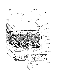
propyl, butyl,
pentyl group or isomer thereof; any alkane, alkene, or alkyne CxHy, where x =
1 - 20, y = 1 -
42, cyclic, branched or straight-chain; alkyl halides, CxHyXz, x = 1 - 20, y =
0 - 42, z = 1 -
42, X = F, Cl, Br, or I; any aromatic group (e.g., phenyl, alkylphenl,
alkoxyphenyl, pyridine,
naphthalene); cyclic complexes where at least one nitrogen is contained within
the ring (e.g.,
octahydropyrimido[1,2-a]pyrimidine, pyrimido[1,2-a]pyrimidine,
hexahydroimidazo[1,2-
a]imidazole, hexahydropyrimidin-2-imine); any sulfur-containing group (e.g.,
sulfoxide,
thiol, alkyl sulfide); any nitrogen-containing group (nitroxide, amine); any
phosphorous
containing group (phosphate); any boron-containing group (e.g., boronic acid);
any organic
acid (acetic acid, propanoic acid) and ester or amide derivatives thereof; any
amino acid (e.g.,
glycine, cysteine, proline, glutamic acid, arginine, serine, histindine, 5-
ammoniumvaleric
acid) including alpha, beta, gamma, and greater derivatives; any silicon
containing group
(e.g., siloxane); and any alkoxy or group, -0CxHy, where x = 0 - 20, y = 1 -
42.
[0060] In certain embodiments, C may include an ethene tetramine cation, an
organic
cation of the general formula [(R2N)2C=C(NR2)2]+ where the R groups can be the
same or
different groups. Suitable R groups include, but are not limited to: hydrogen,
methyl, ethyl,
propyl, butyl, pentyl group or isomer thereof; any alkane, alkene, or alkyne
CxHy, where x =
1 - 20, y = 1 - 42, cyclic, branched or straight-chain; alkyl halides, CxHyXz,
x 1 - 20, y = 0
- 42, z = 1 - 42, X = F, Cl, Br, or I; any aromatic group (e.g., phenyl,
alkylphenl,
alkoxyphenyl, pyridine, naphthalene); cyclic complexes where at least one
nitrogen is
contained within the ring (e.g., 2-hexahydropyrimidin-2-
ylidenehexahydropyrimidine,
octahydropyrazino [2,3 -b]pyrazine, pyrazino [2,3 -b] pyrazine, quinoxalino
[2,3-b] quinoxaline);
any sulfur-containing group (e.g., sulfoxide, thiol, alkyl sulfide); any
nitrogen-containing
group (nitroxide, amine); any phosphorous containing group (phosphate); any
boron-
containing group (e.g., boronic acid); any organic acid (acetic acid,
propanoic acid) and ester
or amide derivatives thereof; any amino acid (e.g., glycine, cysteine,
proline, glutamic acid,
17
CA 02931692 2016-05-25
WO 2015/080990 PCT/US2014/067024
arginine, serine, histindine, 5-ammoniumvaleric acid) including alpha, beta,
gamma, and
greater derivatives; any silicon containing group (e.g., siloxane); and any
alkoxy or group, -
0CxHy, where x = 0 - 20, y = 1 - 42.
[0061] In some embodiments, X may include one or more halides. In certain
embodiments, X may instead or in addition include a Group 16 anion. In certain
embodiments, the Group 16 anion may be sulfide or selenide. In some
embodiments, each
organic cation C may be larger than each metal M, and each anion X may be
capable of
bonding with both a cation C and a metal M. Examples of perovskite materials
according to
various embodiments include CsSnI3 (previously discussed herein) and CsxSnyI,
(with x, y,
and z varying in accordance with the previous discussion). Other examples
include
compounds of the general fointula CsSnX3, where X may be any one or more of:
13, 12 95F0 05;
12C1; 1C12; and C13. In other embodiments, X may comprise any one or more of
I, Cl, F, and
Br in amounts such that the total ratio of X as compared to Cs and Sn results
in the general
stoichiometry of CsSnX3. In some embodiments, the combined stoichiometry of
the elements
that constitute X may follow the same rules as Iz as previously discussed with
respect to
CsxSnyIz. Yet other examples include compounds of the general formula
RNH3PbX3, where
R may be Cnll2n+1, with n ranging from 0-10, and X may include any one or more
of F, Cl,
Br, and I in amounts such that the total ratio of X as compared to the cation
RNH3 and metal
Pb results in the general stoichiometry of RNH3PbX3. Further, some specific
examples of R
include H, alkyl chains (e.g., CH3, CH3CH2, CH3CH2CH2, and so on), and amino
acids (e.g.,
glycine, cysteine, proline, glutamic acid, arginine, serine, histindine, 5-
ammoniumvaleric
acid) including alpha, beta, gamma, and greater derivatives.
[0062] In some embodiments, a perovskite material may be included in a PV or
other
device as active material. For example, one or more perovskite materials may
serve as either
or both of first and second active material of some embodiments (e.g., active
materials 2810
and 2815 of FIG. 5). In more general terms, some embodiments of the present
disclosure
provide PV or other devices having an active layer comprising one or more
perovskite
materials. In such embodiments, perovskite material (that is, material
including any one or
more perovskite materials(s)) may be employed in active layers of various
architectures.
Furthermore, perovskite material may serve the function(s) of any one or more
components
of an active layer (e.g., charge transport material, mesoporous material,
photoactive material,
and/or interfacial material, each of which is discussed in greater detail
below). In some
embodiments, the same perovskite materials may serve multiple such functions,
although in
other embodiments, a plurality of perovskite materials may be included in a
device, each
18
CA 02931692 2016-05-25
WO 2015/080990 PCT/US2014/067024
perovskite material serving one or more such functions. In certain
embodiments, whatever
role a perovskite material may serve, it may be prepared and/or present in a
device in various
states. For example, it may be substantially solid in some embodiments. In
other
embodiments, it may be a solution (e.g., perovskite material may be dissolved
in liquid and
present in said liquid in its individual ionic subspecies); or it may be a
suspension (e.g., of
perovskite material particles). A solution or suspension may be coated or
otherwise
deposited within a device (e.g., on another component of the device such as a
mesoporous,
interfacial, charge transport, photoactive, or other layer, and/or on an
electrode). Perovskite
materials in some embodiments may be formed in situ on a surface of another
component of a
device (e.g., by vapor deposition as a thin-film solid). Any other suitable
means of forming a
solid or liquid layer comprising perovskite material may be employed.
[0063] In general, a perovskite material device may include a first electrode,
a second
electrode, and an active layer comprising a perovskite material, the active
layer disposed at
least partially between the first and second electrodes. In some embodiments,
the first
electrode may be one of an anode and a cathode, and the second electrode may
be the other of
an anode and cathode. An active layer according to certain embodiments may
include any
one or more active layer components, including any one or more of: charge
transport
material; liquid electrolyte; mesoporous material; photoactive material (e.g.,
a dye, silicon,
cadmium telluride, cadmium sulfide, cadmium selenide, copper indium gallium
selenide,
gallium arsenide, germanium indium phosphide, semiconducting polymers, other
photoactive
materials)); and interfacial material. Any one or more of these active layer
components may
include one or more perovskite materials. In some embodiments, some or all of
the active
layer components may be in whole or in part arranged in sub-layers. For
example, the active
layer may comprise any one or more of: an interfacial layer including
interfacial material; a
mesoporous layer including mesoporous material; and a charge transport layer
including
charge transport material. In some embodiments, photoactive material such as a
dye may be
coated on, or otherwise disposed on, any one or more of these layers. In
certain
embodiments, any one or more layers may be coated with a liquid electrolyte.
Further, an
interfacial layer may be included between any two or more other layers of an
active layer
according to some embodiments, and/or between a layer and a coating (such as
between a dye
and a mesoporous layer), and/or between two coatings (such as between a liquid
electrolyte
and a dye), and/or between an active layer component and an electrode.
Reference to layers
herein may include either a final arrangement (e.g., substantially discrete
portions of each
material separately definable within the device), and/or reference to a layer
may mean
19
CA 02931692 2016-05-25
WO 2015/080990 PCT/US2014/067024
arrangement during construction of a device, notwithstanding the possibility
of subsequent
intermixing of material(s) in each layer. Layers may in some embodiments be
discrete and
comprise substantially contiguous material (e.g., layers may be as
stylistically illustrated in
FIG. 1). In other embodiments, layers may be substantially intermixed (as in
the case of, e.g.,
BHJ, hybrid, and some DSSC cells), an example of which is shown by first and
second active
material 2618 and 2620 within photoactive layer 2616 in FIG. 4. In some
embodiments, a
device may comprise a mixture of these two kinds of layers, as is also shown
by the device of
FIG. 4, which contains discrete contiguous layers 2627, 2626, and 2622, in
addition to a
photoactive layer 2616 comprising intermixed layers of first and second active
material 2618
and 2620. In any case, any two or more layers of whatever kind may in certain
embodiments
be disposed adjacent to each other (and/or intermixedly with each other) in
such a way as to
achieve a high contact surface area. In certain embodiments, a layer
comprising perovskite
material may be disposed adjacent to one or more other layers so as to achieve
high contact
surface area (e.g., where a perovskite material exhibits low charge mobility).
In other
embodiments, high contact surface area may not be necessary (e.g., where a
perovskite
material exhibits high charge mobility).
[0064] A perovskite material device according to some embodiments may
optionally
include one or more substrates. In some embodiments, either or both of the
first and second
electrode may be coated or otherwise disposed upon a substrate, such that the
electrode is
disposed substantially between a substrate and the active layer. The materials
of composition
of devices (e.g., substrate, electrode, active layer and/or active layer
components) may in
whole or in part be either rigid or flexible in various embodiments. In some
embodiments, an
electrode may act as a substrate, thereby negating the need for a separate
substrate.
[0065] Furthermore, a perovskite material device according to certain
embodiments
may optionally include light-harvesting material (e.g., in a light-harvesting
layer, such as
Light Harvesting Layer 1601 as depicted in the exemplary PV represented in
FIG. 2). In
addition, a perovskite material device may include any one or more additives,
such as any
one or more of the additives discussed above with respect to some embodiments
of the
present disclosure.
[0066] Description of some of the various materials that may be included in a
perovskite material device will be made in part with reference to FIG. 9. FIG.
9 is a stylized
diagram of a perovskite material device 3900 according to some embodiments.
Although
various components of the device 3900 are illustrated as discrete layers
comprising
contiguous material, it should be understood that FIG. 9 is a stylized
diagram; thus,
CA 02931692 2016-05-25
WO 2015/080990 PCT/US2014/067024
embodiments in accordance with it may include such discrete layers, and/or
substantially
intermixed, non-contiguous layers, consistent with the usage of "layers"
previously discussed
herein. The device 3900 includes first and second substrates 3901 and 3913. A
first
electrode 3902 is disposed upon an inner surface of the first substrate 3901,
and a second
electrode 3912 is disposed on an inner surface of the second substrate 3913.
An active layer
3950 is sandwiched between the two electrodes 3902 and 3912. The active layer
3950
includes a mesoporous layer 3904; first and second photoactive materials 3906
and 3908; a
charge transport layer 3910, and several interfacial layers. FIG. 9
furthermore illustrates an
example device 3900 according to embodiments wherein sub-layers of the active
layer 3950
are separated by the interfacial layers, and further wherein interfacial
layers are disposed
upon each electrode 3902 and 3912. In particular, second, third, and fourth
interfacial layers
3905, 3907, and 3909 are respectively disposed between each of the mesoporous
layer 3904,
first photoactive material 3906, second photoactive material 3908, and charge
transport layer
3910. First and fifth interfacial layers 3903 and 3911 are respectively
disposed between (i)
the first electrode 3902 and mesoporous layer 3904; and (ii) the charge
transport layer 3910
and second electrode 3912. Thus, the architecture of the example device
depicted in FIG. 9
may be characterized as: substrate¨electrode¨active layer¨electrode¨substrate.
The
architecture of the active layer 3950 may be characterized as: interfacial
layer¨mesoporous
layer¨interfacial layer¨photoactive material¨interfacial layer¨photoactive
material¨
interfacial layer¨charge transport layer¨interfacial layer. As noted
previously, in some
embodiments, interfacial layers need not be present; or, one or more
interfacial layers may be
included only between certain, but not all, components of an active layer
and/or components
of a device.
[0067] A substrate, such as either or both of first and second substrates 3901
and
3913, may be flexible or rigid. If two substrates are included, at least one
should be
transparent or translucent to electromagnetic (EM) radiation (such as, e.g.,
UV, visible, or IR
radiation). If one substrate is included, it may be similarly transparent or
translucent,
although it need not be, so long as a portion of the device permits EM
radiation to contact the
active layer 3950. Suitable substrate materials include any one or more of:
glass; sapphire;
magnesium oxide (MgO); mica; polymers (e.g., PET, PEG, polypropylene,
polyethylene,
etc.); ceramics; fabrics (e.g., cotton, silk, wool); wood; drywall; metal; and
combinations
thereof.
[0068] As previously noted, an electrode (e.g., one of electrodes 3902 and
3912 of
FIG. 9) may be either an anode or a cathode. In some embodiments, one
electrode may
21
CA 02931692 2016-05-25
WO 2015/080990 PCT/US2014/067024
function as a cathode, and the other may function as an anode. Either or both
electrodes 3902
and 3912 may be coupled to leads, cables, wires, or other means enabling
charge transport to
and/or from the device 3900. An electrode may constitute any conductive
material, and at
least one electrode should be transparent or translucent to EM radiation,
and/or be arranged in
a manner that allows EM radiation to contact at least a portion of the active
layer 3950.
Suitable electrode materials may include any one or more of: indium tin oxide
or tin-doped
indium oxide (ITO); fluorine-doped tin oxide (FT0); cadmium oxide (CdO); zinc
indium tin
oxide (ZITO); aluminum zinc oxide (AZO); aluminum (Al); gold (Au); calcium
(Ca);
magnesium (Mg); titanium (Ti); steel; carbon (and allotropes thereof); and
combinations
thereof.
[0069] Mesoporous material (e.g., the material included in mesoporous layer
3904 of
FIG. 9) may include any pore-containing material. In some embodiments, the
pores may
have diameters ranging from about 1 to about 100 nm; in other embodiments,
pore diameter
may range from about 2 to about 50 nm. Suitable mesoporous material includes
any one or
more of: any interfacial material and/or mesoporous material discussed
elsewhere herein;
aluminum (Al); bismuth (Bi); indium (In); molybdenum (Mo); niobium (Nb);
nickel (Ni);
silicon (Si); titanium (Ti); vanadium (V); zinc (Zn); zirconium (Zr); an oxide
of any one or
more of the foregoing metals (e.g., alumina, ceria, titania, zinc oxide,
zircona, etc.); a sulfide
of any one or more of the foregoing metals; a nitride of any one or more of
the foregoing
metals; and combinations thereof.
[0070] Photoactive material (e.g., first or second photoactive material 3906
or 3908 of
FIG. 9) may comprise any photoactive compound, such as any one or more of
silicon (in
some instances, single-crystalline silicon), cadmium telluride, cadmium
sulfide, cadmium
selenide, copper indium gallium selenide, gallium arsenide, germanium indium
phosphide,
one or more semiconducting polymers, and combinations thereof. In certain
embodiments,
photoactive material may instead or in addition comprise a dye (e.g., N719,
N3, other
ruthenium-based dyes). In some embodiments, a dye (of whatever composition)
may be
coated onto another layer (e.g., a mesoporous layer and/or an interfacial
layer). In some
embodiments, photoactive material may include one or more perovskite
materials.
Perovskite-material-containing photoactive substance may be of a solid form,
or in some
embodiments it may take the form of a dye that includes a suspension or
solution comprising
perovskite material. Such a solution or suspension may be coated onto other
device
components in a manner similar to other dyes. In some embodiments, solid
perovskite-
containing material may be deposited by any suitable means (e.g., vapor
deposition, solution
22
CA 02931692 2016-05-25
WO 2015/080990
PCT/US2014/067024
deposition, direct placement of solid material, etc.).
Devices according to various
embodiments may include one, two, three, or more photoactive compounds (e.g.,
one, two,
three, or more perovskite materials, dyes, or combinations thereof). In
certain embodiments
including multiple dyes or other photoactive materials, each of the two or
more dyes or other
photoactive materials may be separated by one or more interfacial layers. In
some
embodiments, multiple dyes and/or photoactive compounds may be at least in
part
intermixed.
[0071] Charge transport material (e.g., charge transport material of charge
transport
layer 3910 in FIG. 9) may include solid-state charge transport material (i.e.,
a colloquially
labeled solid-state electrolyte), or it may include a liquid electrolyte
and/or ionic liquid. Any
of the liquid electrolyte, ionic liquid, and solid-state charge transport
material may be referred
to as charge transport material. As used herein, "charge transport material"
refers to any
material, solid, liquid, or otherwise, capable of collecting charge carriers
and/or transporting
charge carriers. For instance, in PV devices according to some embodiments, a
charge
transport material may be capable of transporting charge carriers to an
electrode. Charge
carriers may include holes (the transport of which could make the charge
transport material
just as properly labeled "hole transport material") and electrons. Holes may
be transported
toward an anode, and electrons toward a cathode, depending upon placement of
the charge
transport material in relation to either a cathode or anode in a PV or other
device. Suitable
examples of charge transport material according to some embodiments may
include any one
or more of: perovskite material; I/13"; Co complexes; polythiophenes (e.g.,
poly(3-
hexylthiophene) and derivatives thereof, or P3HT); carbazole-based copolymers
such as
polyheptadecanylcarbazole dithienylbenzothiadiazole and derivatives thereof
(e.g.,PCDTBT);
other copolymers such as polycyclopentadithiophene¨benzothiadiazole and
derivatives
thereof (e.g., PCPDTBT); poly(triaryl amine) compounds and derivatives thereof
(e.g.,
PTAA); Spiro-OMeTAD; fullerenes and/or fullerene derivatives (e.g., C60,
PCBM); and
combinations thereof. In certain embodiments, charge transport material may
include any
material, solid or liquid, capable of collecting charge carriers (electrons or
holes), and/or
capable of transporting charge carriers. Charge transport material of some
embodiments
therefore may be n- or p-type active and/or semi-conducting material. Charge
transport
material may be disposed proximate to one of the electrodes of a device. It
may in some
embodiments be disposed adjacent to an electrode, although in other
embodiments an
interfacial layer may be disposed between the charge transport material and an
electrode (as
shown, e.g., in FIG. 9 with the fifth interfacial layer 3911). In certain
embodiments, the type
23
CA 02931692 2016-05-25
WO 2015/080990 PCT/US2014/067024
of charge transport material may be selected based upon the electrode to which
it is
proximate. For example, if the charge transport material collects and/or
transports holes, it
may be proximate to an anode so as to transport holes to the anode. However,
the charge
transport material may instead be placed proximate to a cathode, and be
selected or
constructed so as to transport electrons to the cathode.
[0072] As previously noted, devices according to various embodiments may
optionally include an interfacial layer between any two other layers and/or
materials,
although devices according to some embodiments need not contain any
interfacial layers.
Thus, for example, a perovskite material device may contain zero, one, two,
three, four, five,
or more interfacial layers (such as the example device of FIG. 9, which
contains five
interfacial layers 3903, 3905, 3907, 3909, and 3911). An interfacial layer may
include a thin-
coat interfacial layer in accordance with embodiments previously discussed
herein (e.g.,
comprising alumina and/or other metal-oxide particles, and/or a titania/metal-
oxide bilayer,
and/or other compounds in accordance with thin-coat interfacial layers as
discussed
elsewhere herein). An interfacial layer according to some embodiments may
include any
suitable material for enhancing charge transport and/or collection between two
layers or
materials; it may also help prevent or reduce the likelihood of charge
recombination once a
charge has been transported away from one of the materials adjacent to the
interfacial layer.
Suitable interfacial materials may include any one or more of: any mesoporous
material
and/or interfacial material discussed elsewhere herein; Al; Bi; In; Mo; Ni;
platinum (Pt); Si;
Ti; V; Nb; Zn; Zr; oxides of any of the foregoing metals (e.g., alumina,
silica, titania); a
sulfide of any of the foregoing metals; a nitride of any of the foregoing
metals; functionalized
or non-functionalized alkyl silyl groups; graphite; graphene; fullerenes;
carbon nanotubes;
and combinations thereof (including, in some embodiments, bilayers of combined
materials).
In some embodiments, an interfacial layer may include perovskite material.
[0073] A device according to the stylized representation of FIG. 9 may in some
embodiments be a PV, such as a DSSC, BHJ, or hybrid solar cell. In some
embodiments,
devices according to FIG. 9 may constitute parallel or serial multi-cell PVs,
batteries, hybrid
PV batteries, FETs, LEDS, and/or any other device discussed herein. For
example, a BHJ of
some embodiments may include two electrodes corresponding to electrodes 3902
and 3912,
and an active layer comprising at least two materials in a heterojunction
interface (e.g., any
two of the materials and/or layers of active layer 3950). In certain
embodiments, other
devices (such as hybrid PV batteries, parallel or serial multi-cell PVs, etc.)
may comprise an
active layer including a perovskite material, corresponding to active layer
3950 of FIG. 9. In
24
CA 02931692 2016-05-25
WO 2015/080990 PCT/US2014/067024
short, the stylized nature of the depiction of the exemplar device of FIG. 9
should in no way
limit the permissible structure or architecture of devices of various
embodiments in
accordance with FIG. 9.
[0074] Additional, more specific, example embodiments of perovskite devices
will be
discussed in terms of further stylized depictions of example devices. The
stylized nature of
these depictions, FIGs. 11-12, similarly is not intended to restrict the type
of device which
may in some embodiments be constructed in accordance with any one or more of
FIGs. 11-
12. That is, the architectures exhibited in FIGs. 11-12 may be adapted so as
to provide the
BHJs, batteries, FETs, hybrid PV batteries, serial multi-cell PVs, parallel
multi-cell PVs and
other similar devices of other embodiments of the present disclosure, in
accordance with any
suitable means (including both those expressly discussed elsewhere herein, and
other suitable
means, which will be apparent to those skilled in the art with the benefit of
this disclosure).
[0075] FIG. 10 depicts an example device 4100 in accordance with various
embodiments. The device 4100 illustrates embodiments including first and
second glass
substrates 4101 and 4109. Each glass substrate has an FTO electrode disposed
upon its inner
surface (first electrode 4102 and second electrode 4108, respectively), and
each electrode has
an interfacial layer deposited upon its inner surface: TiO2 first interfacial
layer 4103 is
deposited upon first electrode 4102, and Pt second interfacial layer 4107 is
deposited upon
second electrode 4108. Sandwiched between the two interfacial layers are: a
mesoporous
layer 4104 (comprising Ti02); photoactive material 4105 (comprising the
perovskite material
MAPbI3); and a charge transport layer 4106 (here comprising CsSnI3).
[0076] FIG. 11 depicts an example device 4300 that omits a mesoporous layer.
The
device 4300 includes a perovskite material photoactive compound 4304
(comprising
MAPbI3) sandwiched between first and second interfacial layers 4303 and 4305
(comprising
titania and alumina, respectively). The titania interfacial layer 4303 is
coated upon an FTO
first electrode 4302, which in turn is disposed on an inner surface of a glass
substrate 4301.
The spiro-OMeTAD charge transport layer 4306 is coated upon an alumina
interfacial layer
4305 and disposed on an inner surface of a gold second electrode 4307.
[0077] As will be apparent to one of ordinary skill in the art with the
benefit of this
disclosure, various other embodiments are possible, such as a device with
multiple
photoactive layers (as exemplified by photoactive layers 3906 and 3908 of the
example
device of FIG. 9). In some embodiments, as discussed above, each photoactive
layer may be
separated by an interfacial layer (as shown by third interfacial layer 3907 in
FIG. 9).
Furthermore, a mesoporous layer may be disposed upon an electrode such as is
illustrated in
CA 02931692 2016-05-25
WO 2015/080990
PCT/US2014/067024
FIG. 9 by mesoporous layer 3904 being disposed upon first electrode 3902.
Although FIG. 9
depicts an intervening interfacial layer 3903 disposed between the two, in
some embodiments
a mesoporous layer may be disposed directly on an electrode.
[0078] Additional Perovskite Material Device Examples
[0079] Other example perovskite material device architectures will be apparent
to
those of skill in the art with the benefit of this disclosure. Examples
include, but are not
limited to, devices containing active layers having any of the following
architectures:
(1) liquid electrolyte¨perovskite material¨mesoporous layer; (2) perovskite
material¨
dye¨mesoporous layer; (3) first perovskite material¨second perovskite
material¨
mesoporous layer; (4) first perovskite material¨second perovskite material;
(5) first
perovskite material¨dye--second perovskite material; (6) solid-state charge
transport
material¨perovskite material; (7) solid-state charge transport material __
dye¨perovskite
material¨mesoporous layer; (8) solid-state charge transport
material¨perovskite material¨
dye¨mesoporous layer; (9) solid-state charge transport material¨dye¨perovskite
material¨mesoporous layer; and (10) solid-state charge transport
material¨perovskite
material¨dye¨mesoporous layer. The individual components of each example
architecture
(e.g., mesoporous layer, charge transport material, etc.) may be in accordance
with the
discussion above for each component. Furthermore, each example architecture is
discussed
in more detail below.
[0080] As a particular example of some of the aforementioned active layers, in
some
embodiments, an active layer may include a liquid electrolyte, perovskite
material, and a
mesoporous layer. The active layer of certain of these embodiments may have
substantially
the architecture: liquid electrolyte¨perovskite material¨mesoporous layer. Any
liquid
electrolyte may be suitable; and any mesoporous layer (e.g., Ti02) may be
suitable. In some
embodiments, the perovskite material may be deposited upon the mesoporous
layer, and
thereupon coated with the liquid electrolyte. The perovskite material of some
such
embodiments may act at least in part as a dye (thus, it may be photoactive).
[0081] In other example embodiments, an active layer may include perovskite
material, a dye, and a mesoporous layer. The active layer of certain of these
embodiments
may have substantially the architecture: perovskite material¨dye¨mesoporous
layer. The
dye may be coated upon the mesoporous layer and the perovskite material may be
disposed
upon the dye-coated mesoporous layer. The perovskite material may function as
hole-
transport material in certain of these embodiments.
26
CA 02931692 2016-05-25
WO 2015/080990 PCT/US2014/067024
[0082] In yet other example embodiments, an active layer may include first
perovskite material, second perovskite material, and a mesoporous layer. The
active layer of
certain of these embodiments may have substantially the architecture: first
perovskite
material¨second perovskite material¨mesoporous layer. The first and second
perovskite
material may each comprise the same perovskite material(s) or they may
comprise different
perovskite materials. Either of the first and second perovskite materials may
be photoactive
(e.g., a first and/or second perovskite material of such embodiments may
function at least in
part as a dye).
[0083] In certain example embodiments, an active layer may include first
perovskite
material and second perovskite material. The active layer of certain of these
embodiments
may have substantially the architecture: first perovskite material¨second
perovskite
material. The first and second perovskite materials may each comprise the same
perovskite
material(s) or they may comprise different perovskite materials. Either of the
first and
second perovskite materials may be photoactive (e.g., a first and/or second
perovskite
material of such embodiments may function at least in part as a dye). In
addition, either of
the first and second perovskite materials may be capable of functioning as
hole-transport
material. In some embodiments, one of the first and second perovskite
materials functions as
an electron-transport material, and the other of the first and second
perovskite materials
functions as a dye. In some embodiments, the first and second perovskite
materials may be
disposed within the active layer in a manner that achieves high interfacial
area between the
first perovskite material and the second perovskite material, such as in the
arrangement
shown for first and second active material 2810 and 2815, respectively, in
FIG. 5 (or as
similarly shown by p- and n-type material 2618 and 2620, respectively, in FIG.
4).
[0084] In further example embodiments, an active layer may include first
perovskite
material, a dye, and second perovskite material. The active layer of certain
of these
embodiments may have substantially the architecture: first perovskite
material¨dye¨second
perovskite material. Either of the first and second perovskite materials may
function as
charge transport material, and the other of the first and second perovskite
materials may
function as a dye. In some embodiments, both of the first and second
perovskite materials
may at least in part serve overlapping, similar, and/or identical functions
(e.g., both may
serve as a dye and/or both may serve as hole-transport material).
[0085] In some other example embodiments, an active layer may include a solid-
state
charge transport material and a perovskite material. The active layer of
certain of these
embodiments may have substantially the architecture: solid-state charge
transport material-
27
CA 02931692 2016-05-25
WO 2015/080990 PCT/US2014/067024
perovskite material. For example, the perovskite material and solid-state
charge transport
material may be disposed within the active layer in a manner that achieves
high interfacial
area, such as in the arrangement shown for first and second active material
2810 and 2815,
respectively, in FIG. 5 (or as similarly shown by p- and n-type material 2618
and 2620,
respectively, in FIG. 4).
[0086] In other example embodiments, an active layer may include a solid-state
charge transport material, a dye, perovskite material, and a mesoporous layer.
The active
layer of certain of these embodiments may have substantially the architecture:
solid-state
charge transport material dye¨perovskite material¨mesoporous layer. The
active layer of
certain other of these embodiments may have substantially the architecture:
solid-state charge
transport material¨perovskite material¨dye¨mesoporous layer. The perovskite
material
may in some embodiments serve as a second dye. The perovskite material may in
such
embodiments increase the breadth of the spectrum of visible light absorbed by
a PV or other
device including an active layer of such embodiments. In certain embodiments,
the
perovskite material may also or instead serve as an interfacial layer between
the dye and
mesoporous layer, and/or between the dye and the charge transport material.
[0087] In some example embodiments, an active layer may include a liquid
electrolyte, a dye, a perovskite material, and a mesoporous layer. The active
layer of certain
of these embodiments may have substantially the architecture: solid-state
charge transport
material¨dye¨perovskite material¨mesoporous layer. The active layer of certain
other of
these embodiments may have substantially the architecture: solid-state charge
transport
material¨perovskite material¨dye¨mesoporous layer. The perovskite material may
serve
as photoactive material, an interfacial layer, and/or a combination thereof.
[0088] Some embodiments provide BHJ PV devices that include perovskite
materials.
For example, a BHJ of some embodiments may include a photoactive layer (e.g.,
photoactive
layer 2404 of FIG. 3), which may include one or more perovskite materials. The
photoactive
layer of such a BHJ may also or instead include any one or more of the above-
listed example
components discussed above with respect to DSSC active layers. Further, in
some
embodiments, the BHJ photoactive layer may have an architecture according to
any one of
the exemplary embodiments of DSSC active layers discussed above.
[0089] In some embodiments, any PV or other like device may include an active
layer
according to any one or more of the compositions and/or architectures
discussed above. For
example, an active layer including perovskite material may be included in a
hybrid PV
battery, for example as PV Active Layer 3603 of the exemplary hybrid PV
battery depicted in
28
CA 02931692 2016-05-25
WO 2015/080990 PCT/US2014/067024
FIG. 6, and/or as Battery Active Layer 3605 of FIG. 6. As another example
embodiment, an
active layer including perovskite material may be included in a multi-
photoactive-layer PV
cell, such as either or both of the first and second photoactive layers 3701
and 3705 of the
exemplary cell shown in the stylized diagram of FIG. 7. Such a multi-
photoactive-layer PV
cell including an active layer with perovskite material could furthermore be
incorporated
within a series of electrically coupled multi-photoactive-layer PV cells (in
some
embodiments, in accordance with the structure as shown, e.g., in FIG. 8A).
[0090] In some embodiments, any of the active layers including perovskite
materials
incorporated into PVs or other devices as discussed herein may further include
any of the
various additional materials also discussed herein as suitable for inclusion
in an active layer.
For example, any active layer including perovskite material may further
include an interfacial
layer according to various embodiments discussed herein (such as, e.g., a thin-
coat interfacial
layer). By way of further example, an active layer including perovskite
material may further
include a light harvesting layer, such as Light Harvesting Layer 1601 as
depicted in the
exemplary PV represented in FIG. 2.
[0091] Therefore, the present invention is well adapted to attain the ends and
advantages mentioned as well as those that are inherent therein. The
particular embodiments
disclosed above are illustrative only, as the present invention may be
modified and practiced
in different but equivalent manners apparent to those skilled in the art
having the benefit of
the teachings herein. Furthermore, no limitations are intended to the details
of construction
or design herein shown, other than as described in the claims below. It is
therefore evident
that the particular illustrative embodiments disclosed above may be altered or
modified and
all such variations are considered within the scope and spirit of the present
invention. In
particular, every range of values (of the form, "from about a to about b," or,
equivalently,
"from approximately a to b," or, equivalently, "from approximately a-b")
disclosed herein is
to be understood as referring to the power set (the set of all subsets) of the
respective range of
values, and set forth every range encompassed within the broader range of
values. Also, the
terms in the claims have their plain, ordinary meaning unless otherwise
explicitly and clearly
defined by the patentee.
29