Note: Descriptions are shown in the official language in which they were submitted.
CA 02932698 2016-06-10
- 1 -
BIDIRECTIONAL MOSFET SWITCH AND MULTIPLEXER
The invention relates to a bidirectional MOSFET switch and a multiplexer
comprising at least two bidirectional MOSFET switches.
The present circuit topology is based on an already known MOSFET circuit
topology for bidirectional signal interconnection that is also referred to as
"common source" and is illustrated in figure 1.
In order to switch the transistors into the on state, a control current is
necessary
which generates the required gate-source voltage across the resistor R1 and
charges the input capacitances of the two gates Ti and T2. If this control
voltage is galvanically coupled to the signal voltage, it must be greater or
less
than the signal voltage depending on MOSFET types used (N- or P-channel),
within the scope of the transistor specification, in order that Ti and T2 can
be
switched into the on state. This may be technically difficult in the case of
high-
voltage signals. What is also disadvantageous is that the control current can
be
superposed with the signal current and flows via the terminals A or B to the
opposite potential. As a result, this circuit variant is unfavorable for an
interconnection of measurement voltage signals.
Therefore, here the control current is often generated photovoltaically (see
figure 2), which firstly provides for the galvanic isolation for the purpose
of
driving and secondly prevents the control current from being superposed with
the signal current. What is disadvantageous here is that the driving of the
gates
of Ti and T2 requires a relatively high control current which must primarily
first
of all supply the LED1. The control current generated on the secondary side,
e.g. from a photodiode (D1), is relatively small, which is an obstacle to
rapidly
switching on Ti and T2.
If this type of switch is required multiply, for example in a realization of a
multiplexer, this type of galvanically isolated driving has to be realized
individually for each transistor pair. This is technically complex.
CA 02932698 2016-06-10
- 2 -
In test engineering and metrology, for example for automated connection
testers, there is the objective of interconnecting signal voltages and
currents by
means of a switching matrix which consists of up to several thousand
individual
switches and has to interconnect currents up to well within the amperes range
and voltages of up to a few kilovolts. If the signal voltage is a dangerous
contact
voltage, the stipulations for air clearances and creepage paths and insulation
from the respectively relevant safety standard (e.g. IEC60950, IEC61010 etc.)
must be complied with for each driving for safety reasons, in order to
reliably
isolate driving and switches from one another. The large distances, owing to
the mixed construction of switching element, on the one hand, and drive lines,
on the other hand, which must also be insulated from the other switching
elements of the matrix, make it more difficult to implement the construction
with
a high packing density, which makes the construction more expensive, or
causes the construction to become larger.
A further variant for galvanic isolation in relation to the photovoltaic
driving is
capacitive driving, by means of two small capacitors. However, the latter can
only transmit AC signals, which then ultimately have to be rectified again in
order to supply the required gate-source voltage for Ti and T2.
Furthermore, the complex, expensive variant of driving by means of a
transformer is known. Here as well only AC signals can be transmitted, which
then have to be rectified on the secondary side.
The galvanic isolation during driving prevents the drive current from being
superposed with the current to be interconnected and allows the drive voltage
to be able to have a different potential than the signal voltage. A technical
difficulty is posed here by the energy to be transmitted, which has to be
transmitted as efficiently as possible via the galvanic isolation in order to
charge
the gates of the two transistors Ti and T2, in order that the latter can
switch
into the on state rapidly enough. In conventional driving by means of
photovoltaics, a relatively large amount of energy is required in order to
compensate for the losses of the LED-receiver diode coupling section, which
CA 02932698 2016-06-10
- 3 -
would lead to high power losses in the case of a multiplexer arrangement
having many switches.
The invention is based on the object, then, of improving a bidirectional
MOSFET
circuit topology.
This object is achieved by means of a bidirectional MOSFET switch as claimed
in claim 1 and a multiplexer as claimed in claim 11.
The bidirectional MOSFET switch according to the invention comprises an input
and an output and two MOSFET transistors, which are connected to one
another by their source and gate terminals, wherein the input and the output
are connected to a respective drain terminal of the two MOSFET transistors,
and comprises a control input galvanically isolated by means of a potential
isolation, said control input being connected to a control unit configured to
switch a control current for a FET transistor via a further MOSFET transistor,
said FET transistor being configured to generate, by means of the control
current, a gate voltage Vgs between gate and source at the two MOSFET
transistors for the switching thereof, and a floating voltage source, which is
galvanically connected to the input and is configured to generate a gate
control
current for the two MOSFET transistors.
The bidirectional MOSFET switch according to the invention has the advantage
that even for AC voltage signals a low control current is sufficient for the
circuit
topology.
The FET transistor may be configured to convert the control current into a
gate-
source voltage, by means of a current saturation and a high-resistance state
brought about thereby, in order to switch on the two MOSFET transistors. Said
control current is limited by the FET transistor by virtue of the latter
attaining
saturation. It then constitutes a high-resistance constant-current source. In
this
regard, an increased switch-on current flows only momentarily until the gates
of Ti and T2 are charged.
CA 02932698 2016-06-10
- 4 -
The FET transistor in a state in which a control current does not flow through
may be configured to connect the gates of the two MOSFET transistors to the
source of the two MOSFET transistors at low resistance, in order to switch off
the two MOSFET transistors. The low resistance of the FET transistor has the
advantage that when interconnecting AC signals only correspondingly small RC
elements with the parasitic capacitances of Ti and T2 are formed and so the
leakage current behavior is improved by virtue of the fact that the Vgs of Ti
and
T2 can be kept below the transistor threshold voltage more reliably.
The floating voltage source or floating voltage supply may be galvanically
connected to one of the two drain terminals of the two MOSFET transistors.
This allows a simple realization of the supply for the control unit. The
floating
voltage source may be the secondary side of a DC/DC converter, a battery or
a voltage generated by a generator, for example by an energy harvester or a
solar cell.
The floating voltage source may be the voltage and/or current supply for the
control unit, which simplifies the circuit construction.
The floating voltage source may be configured to generate the control current
in order to control the FET transistor at high resistance and to charge the
gate
capacitances of the two MOSFET transistors. In this regard, an increased
switch-on current flows only momentarily until the gates of Ti and T2 are
charged. As a result, the transistors Ti and T2 are switched into the on state
more rapidly.
The control unit may be configured to store the switching state of the further
MOSFET transistor. In the simplest case, the control unit may be a flip-flop
that
stores the switching state of the analog switch. This allows simple
bidirectional
switching.
The further MOSFET transistor may be configured to switch the gate control
current of the floating voltage source depending on the stored switching state
of the control unit. This allows simple bidirectional switching.
CA 02932698 2016-06-10
- 5 -
The two MOSFET transistors may be N-channel types and the floating voltage
source may be connected by its negative potential to the drain terminal of one
of the two MOSFET transistors, or the two MOSFET transistors may be P-
channel types and the floating voltage source may be connected by its positive
potential to the drain terminal of one of the two MOSFET transistors. In this
way, the circuit may be realized in a simple manner for both types of
transistors.
The further MOSFET transistor may be of the P-channel type if the two
MOSFET transistors are N-channel types, or wherein the further MOSFET
transistor is of the N-channel type if the two MOSFET transistors are P-
channel
types. In this way, the circuit may be realized in a simple manner for both
types
of transistors.
The multiplexer according to the invention comprises at least two
bidirectional
MOSFET switches as described above, wherein a potential isolation and a
floating voltage source are provided jointly for all the bidirectional MOSFET
switches. The multiplexer according to the invention has the advantage that
even for AC voltage signals a low control current is sufficient for the
circuit
topology, which allows a high scalability in the case of multiplexers, in
particular
for switching matrices.
The invention is explained below in exemplary embodiments with reference to
the associated drawings, in which:
Figure 1 shows a bidirectional MOSFET switch from the prior art;
Figure 2 shows a bidirectional MOSFET switch with photovoltaically
generated control current from the prior art;
Figure 3 shows a bidirectional MOSFET switch in accordance with one
exemplary embodiment of the invention;
CA 02932698 2016-06-10
- 6 -
Figure 4 shows a multiplexer in accordance with one exemplary
embodiment of the invention;
Figure 5 shows a bidirectional MOSFET switch with snubber in
accordance with one exemplary embodiment of the invention;
and
Figure 6 shows a bidirectional MOSFET switch comprising
complementary transistors in comparison with figure 3 in
accordance with one exemplary embodiment of the invention.
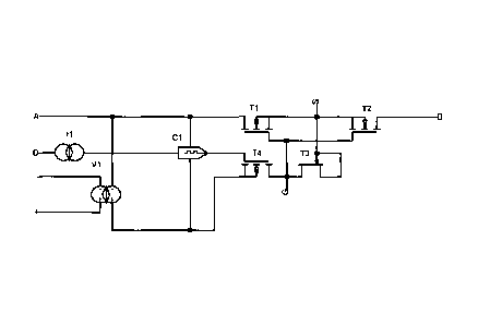
Figure 3 shows a first exemplary embodiment of a bidirectional MOSFET switch
or a circuit topology consisting of two MOSFET transistors Ti and T2. The two
MOSFET transistors Ti and T2 are connected to one another by their source
terminals S and gate terminals G and constitute as it were the actual
bidirectional switching element. The otherwise customary gate-source resistor
is replaced by a FET transistor T3 having a low "pinch off' voltage. The FET
transistor T3 is connected to the source of the two MOSFET transistors Ti and
T2 by its gate terminal and is source terminal. The drain terminal is
connected
.. to the gate of the two MOSFET transistors Ti and T2.
If no drive current flows, the FET transistor T3 constitutes a relatively low-
resistance connection which connects the gate terminals to the source
terminals of Ti and T2. In this regard, the gates are discharged and the two
transistors Ti and T2 are switched into the off state. A resistor having a
high
resistance that is otherwise used, in order to keep the control current low,
would
constitute a disadvantage when interconnecting AC signals since it forms an
RC element with the parasitic capacitances of Ti and T2. This would
disadvantageously influence the leakage current behavior of Ti and T2 in that,
in the case of fast potential shifts at S, the potential at G can no longer be
compensated for by S. This could have the effect that Ti and T2 possibly
already become somewhat conducting as a result of the voltage Vgs produced.
Furthermore, a resistor having a high resistance leads to slower switch-off
times
of Ti and T2.
CA 02932698 2016-06-10
- 7 -
The disadvantages mentioned above are avoided by the use of the FET
transistor T3. Depending on the polarity of the signal voltage it may happen
that
although one of the two "body" diodes of Ti or T2 conducts, one of the two
transistors Ti or T2 is also always switched in the reverse direction, which
ensures that the switch is in the off state independently of polarity.
The circuit topology according to the invention furthermore consists of a
further
circuit part in order to switch the two transistors Ti and T2 into the on
state. A
"floating" voltage supply source V1 is galvanically connected to an input A of
the circuit on the secondary side. This constitutes the supply for a control
unit
or driving unit C1, which in the simplest case is a flip-flop as switching
state
storage unit. Furthermore, the drain terminal of the transistor Ti is
connected
to the input A. The drain terminal of the transistor T2 is connected to an
output
B of the circuit.
The input of the control unit C1 is connected to a drive line or a drive bus D
of
the circuit in which a potential isolation 11 is provided. The output of the
control
unit Cl drives a further MOSFET switching transistor T4. If D is a drive bus,
the
decoding of the drive signal for T4 is also performed in the control unit Cl.
If T4
is switched on, the source V1 drives a control current via T4 to the FET T3.
Said
control current is limited by the FET T3 by virtue of the latter attaining
saturation
and then constituting a high-resistance constant-current source. As a result,
a
higher switch-on current than the constant current established by the FET T3
flows only momentarily at the switch-on instant until the gates of Ti and T2
are
charged. The potential isolation II ensures that the control current flows
only in
the circuit V1, T4, T3, and Ti.
As a result, the transistors Ti and T2 are switched into the on state more
rapidly. This and the drive current that is limited in a controlled manner
constitute an advantage of this circuit in order to keep down the control
current
power loss and the switching power loss of Ti and T2. Via the "body" diode of
Ti, the control current can always flow back to the source V1 even in the off
state of Ti, as a result of which Ti and T2 can always be driven by the
control
current, independently of the potential at S. A further advantage of this
circuit
topology is the fact that the control current can flow from the floating
source V1
CA 02932698 2016-06-10
- 8 -
only in the circuit V1, T4, T3, and Ti and cannot flow via the terminals A or
B
and, consequently, outside the terminals A and B, it is not superposed with
the
signal current.
All components in these circuits mentioned only have to have a sufficiently
high
functional isolation with regard to the signal voltage level, and this is
significantly easier to realize than a safety-relevant isolation with respect
to the
drive lines for dangerous contact voltages. In figure 3, the transistors Ti
and
T2 are embodied as normally off N-channel MOSFET transistors, while the
transistor T4 is embodied as a normally off P-channel MOSFET transistor.
Figure 4 illustrates a circuit topology as a multiplexer, here as a 1:2
multiplexer.
Accordingly, two bidirectional MOSFET switches from figure 3 are provided,
which are connected to the input A in parallel and produce two outputs B and
B1.
Advantageously, the potential isolation 11 is realized centrally for both
driving
units Cl and C2 and for the voltage source V1, for example a DC/DC converter.
This constitutes a significant technical simplification with regard to the
demand
of air clearances and creepage paths, insulation, number of components and
packing density. This is the case in particular for multiplexers having a
large
number of individual switches such as, for example, 1:1000 multiplexers.
The drive line D and the supply voltage V1 can be isolated from the signal
voltage centrally outside the region of a circuit board, separately from the
region
of the interconnection of the signal voltage. Within the "switching region",
as a
result of the galvanic coupling to terminal A, they have the same potential,
or
only a potential that is different as a result of the secondary-side voltage
of V1,
with respect to the signal voltage at A, as a result of which the isolation
requirements relative to A are only very low. This increases the packing
density
of such a switching matrix or makes it functionally more reliable since no
voltage
flashovers from the potential at A to the drive electronics C can occur.
CA 02932698 2016-06-10
- 9 -
For driving the circuit at D only a low power is required since the latter no
longer
has to directly drive the gates of Ti and T2. As a result, the technical
implementation is simplified and the drive power can be reduced.
The potential isolation II ensures that the control current flows only in the
circuit
V1, T4, T3, and Ti. By virtue of the fact that the potential isolation in a
multiplexer arrangement is not needed for each individual switch (in the
extreme case only once per multiplexer) and the signal power is low since the
drive signal at D only has to drive high-resistance inputs, the losses as a
result
of the potential isolation have a less pronounced effect.
The circuit topology according to the invention may be supplemented in a
simple manner by the customary snubbers comprising current-limiting resistors
and voltage-limiting diodes, as is illustrated in figure 5. Such snubbers may
also
be used in the multiplexer in accordance with figure 4. In specific detail, a
zener
diode Z1 is connected between source S and gate G, and a resistor R1 is
connected between source and FET T3, and a resistor R2 is connected
between the further MOSFET T4 and the FET T3 or gate G.
The circuit topology according to the invention may be constructed using
commercially available N- or P-channel MOSFET transistors as switching
transistors Ti and T2; power or high-voltage transistors or HF transistors may
also be involved here. Figure 6 illustrates a complementary choice of
transistors
in comparison with figure 3. Such circuitry arrangements may also be used in
the multiplexer in accordance with figure 4.