Note: Descriptions are shown in the official language in which they were submitted.
CA 2933627 2017-05-11
INTEGRATORS FOR SENSOR APPLICATIONS
Technical Field
[0001] Embodiments herein relate to the field of sensors, and, more
specifically, to the
processing of sensor signals.
Background
[0002] Many medical sensors, such as continuous glucose monitoring (CGM)
sensors include
transimpedance amplifier circuitry for amplifying a sensor current signal.
Such sensors often
include a high resolution analog-to-digital converter (ADC) to further process
the amplified
signal. However, high resolution ADCs are typically more expensive and more
energy intensive
than lower resolution ADCs. Additionally, such sensors typically have low
voltage-per-level and
voltage-to-current ratios, and thus often exhibit undesirable sensitivity to
electrical noise.
[0003] As an example, in order for existing glucose monitoring systems to
achieve the minimum
typically desired resolution of 5 picoamperes/level and cover the full range
of current
magnitudes produced by a CGM sensor (which, for illustrative purposes, may be
approximately
microamperes), an ADC with a dynamic range of (5 microamperes)/(5
picoamperes/level) =
1,000,000 levels is needed, corresponding to a 20-bit ADC (2^20 = 1,048,576).
The
transimpedance amplifier circuitry typically included in such systems often
has a maximum
output voltage of approximately 3 volts. The voltage-to-level ratio of such a
system is then (3
volts)/(1,048,576 levels) = 2.9 microvolts/level. Additionally, the value of
the feedback resistor
included in a transimpedance amplifier is typically selected so that the
maximum range of
voltage outputs are achieved: for a maximum output voltage of 3 volts and a
maximum current of
5 microamperes, the value of the feedback resistor is typically selected to be
as close as possible
to (3 volts)/(5 microamperes) = 600 kiloohms. Assuming that the typical
operating range of
sensor current is 1 picoampere (much lower than the initial 5 microampere
value), the voltage-to-
current ratio under typical operation is (1 picoampere)x(600 kiloohms) = 0.6
microvolts/picoampere. For systems with voltage-to- level and voltage-to-
current ratios this low,
special hardware requirements are typically imposed and expensive components
are typically
used to protect sensitive circuitry from electrical noise.
1
CA 2933627 2017-05-11
Brief Description of the Drawings
[0004] Embodiments will be readily understood by the following detailed
description in
conjunction with tile accompanying drawings and the appended claims.
Embodiments are
illustrated by way of example and not by way of limitation in the figures of
the accompanying
drawings.
[0005] Figure 1 is a block diagram of an electronics assembly including an
integrator circuit and
a reset circuit, in accordance with various aspects;
[0006] Figure 2 illustrates an example sensor signal and corresponding
integrator output signal
that may be generated by an electronics assembly. such as the electronics
assembly of Figure 1,
in accordance with various aspects;
[0007] Figure 3 is a flow diagram of a method of processing a sensor signal,
which may use an
electronics assembly such as the electronics assembly of Figure 1, in
accordance with various
aspects;
[0008] Figure 4 is a schematic diagram of a sensor assembly and an electronics
assembly
including an analog-to-digital converter (ADC), in accordance with various
aspects;
[0009] Figure 5 illustrates an example sensor signal and corresponding
integrator output signal
that may be generated by an electronics assembly, such as the electronics
assembly of Figure 4,
in accordance with various aspects;
[0010] Figure 6 is a flow diagram of a method of determining an integration
interval, in
accordance with various aspects;
[0011] Figure 7 is a schematic diagram of a sensor assembly and an electronics
assembly
including a comparator, in accordance with various aspects;
[0012] Figure 8 is a flow diagram of a method for providing an interrupt
signal, in accordance
with various aspects;
2
CA 2933627 2017-05-11
[0013] Figure 9 illustrates an example sensor signal, corresponding integrator
output signal, and
corresponding interrupt signal that may be generated by an electronics
assembly, such as the
electronics assembly of Figure 7, in accordance with various aspects; and
[0014] Figure 10 is a plan view of an analyte sensor system that may include
any of the sensor
and/or electronics assemblies described herein, in accordance with various
aspects.
Detailed Description
[0015] In the following detailed description, reference is made to the
accompanying drawings
which form a part hereof, and in which are shown by way of illustration
embodiments that may
be practiced. It is to be understood that other aspects and/or embodiments may
be utilized and
structural or logical changes may be made without departing from the scope.
Therefore, the
following detailed description is not to be taken in a limiting sense, and the
scope is defined by
the appended claims and their equivalents.
[0016] Various operations may be described as multiple discrete operations in
turn, in a manner
that may be helpful in understanding the disclosure; however, the order of
description should not
be construed to imply that these operations are order dependent.
[0017] The description may use perspective-based descriptions such as up/down,
back/front, and
top/bottom. Such descriptions are merely used to facilitate the discussion and
are not intended to
restrict the application of the disclosure.
[0018] The terms "coupled'' and "connected," along with their derivatives, may
be used. It
should be understood that these terms are not intended as synonyms for each
other. Rather, in
particular embodiments, "connected" may be used to indicate that two or more
elements are in
direct physical or electrical contact with each other. "Coupled" may mean that
two or more
elements are in direct physical or electrical contact. However, "coupled" may
also mean that two
or more elements are not in direct contact with each other, but yet still
cooperate or interact with
each other.
[0019] For the purposes of the description, a phrase in the form "A/B" or in
the form "A and/or
B" means (A), (B), or (A and B). For the purposes of the description, a phrase
in the form "at
3
CA 2933627 2017-05-11
least one of A, B, and C" means (A), (B), (C), (A and B), (A and C), (B and
C), or (A, B and C).
For the purposes of the description, a phrase in the form "(A)B" means (B) or
(AB) that is, A is
an optional element.
[0020] The description may use the terms "embodiment" or "embodiments," which
may each
refer to one or more of the same or different embodiments. The term "aspect"
generally refers to
features or parts/components of disclosed embodiments. Furthermore, the terms
"comprising,"
"including," "having," and the like, as used with respect to embodiments, are
synonymous, and
are generally intended as "open" terms (e.g., the term "including" should be
interpreted as
"including but not limited to," the term "having" should be interpreted as
"having at least," the
term "includes" should be interpreted as "includes but is not limited to,"
etc.).
[0021] With respect to the use of any plural and/or singular terms herein,
those having skill in
the art can translate from the plural to the singular and/or from the singular
to the plural as is
appropriate to the context and/or application. The various singular/plural
permutations may be
expressly set forth herein for sake of clarity.
[0022] Methods, apparatuses, and systems for processing sensor signals are
provided. A
computing device may be endowed with one or more components of the disclosed
apparatuses
and/or systems and may be employed to perform one or more methods as disclosed
herein. The
embodiments described herein may provide an alternative to traditional
transimpedance
amplifier/high resolution ADC sensors with any of a number of advantages,
including lower
cost, lower power consumption, better noise immunity, or a combination of the
foregoing.
[0023] Various aspects are described in the context of a continuous glucose
monitoring (CGM)
sensor and/or system, although other types of sensors may use the signal
processing methods,
apparatuses and systems described herein. For example, the signal processing
methods,
apparatuses and systems described herein may be used with an electrochemical
blood glucose
monitoring (BGM) sensor and/or system (e.g., during intervals in which the BGM
system
measures an electrochemical property of a blood sample). The signal processing
methods,
apparatuses and systems described herein may be used with an optical blood
glucose monitoring
sensor and/or system (e.g., during intervals in which the optical blood
glucose monitoring system
measures an optical property of a patient's analyte using optical sensors,
such as, but not limited
4
CA 2933627 2017-05-11
to, PIN diodes. In some embodiments, the signal processing methods,
apparatuses and systems
described herein may be applied to an analog signal generated by an
electrochemical BGM
sensor and/or system, and/or an optical blood glucose monitoring sensor and/or
system.
[0024] Figure 1 is a block diagram of an electronics assembly 100 including an
integrator circuit
106 coupled to a reset circuit 108, in accordance with various aspects.
Integrator circuit 106 is
coupled to a sensor contact 102 that is configured to receive a sensor signal
from a sensor
assembly. In some embodiments, the sensor signal provided by the sensor
assembly is
representative of a level of analyte in a body. For example, the sensor
assembly may include a
continuous glucose monitor (CGM) configured to produce the sensor signal. In
some
embodiments, integrator circuit 106 is configured to provide an integrator
output signal
representative of the sensor signal integrated from a first time to a second
time. For example, the
relationship between a sensor current signal Sensor(t) and an integrator
output voltage signal
Out(t) for the configuration of Figure 1 may be given approximately by
ittime2
Out(thne2):',7: ta(t)Sensor(t)-!--13(t))dt (1)
ilne
where a and p are constant or time-varying values. In some embodiments, time]
may be
considered to be the origin of the time axis, in which case time1=0. In some
embodiments, a
constant or additional time-varying term may be added to Eq. 1 (e.g., to
accommodate a non-zero
timel or to address or other constant or time-varying characteristics of
electronics assembly
100).
[00251 Figure 2 illustrates an example sensor signal 202 and corresponding
integrator output
signal 204 that may be generated by an electronics assembly, such as
electronics assembly 100 of
Figure 1. Sensor signal 202 and integrator output signal 204 may be different
types of signals;
for example, sensor signal 202 may be a current signal and integrator output
signal 204 may be a
voltage signal. As shown, integrator output signal 204 is representative of
sensor signal 202
integrated over an integration interval 208 from a first time Ti to a second
time T2. Additionally,
electronics assembly 100 may advantageously provide improved noise immunity
due to the low
pass filter effect of integrator circuit 106. In general, integration time may
be adjusted to achieve
a desired resolution and noise immunity.
CA 2933627 2017-05-11
[0026] Returning to Figure 1, integrator circuit 106 is also coupled to a
processor circuit 114. In
some embodiments, processor circuit 114 is configured to determine a value of
the integrator
output signal provided by integrator circuit 106. Processor circuit 114 may
determine this value
in any of a number of ways, such as by measuring a value of the integrator
output signal (e.g., as
discussed below with reference to Figures 4-6) or by determining an elapsed
time during which
the integrator output signal rose to a threshold value (e.g., as discussed
below with reference to
Figures 7-9).
[0027] Processor circuit 114 is also coupled to reset circuit 1 08. Processor
circuit 114 may
include a processor (e.g., one or more microcontrollers) and supporting
circuitry (e.g., wireless
or wired communications circuitry). In some embodiments, processor circuit 114
is configured to
provide a reset signal to reset circuit 108. In some embodiments, in response
to receiving a reset
signal from processor circuit 114, reset circuit 108 is configured to reset
the integrator output
signal provided by integrator circuit 106. As used herein, "resetting the
integrator output signal"
may refer to causing the integrator output signal to have a predetermined zero
or nonzero value.
Reset circuit 108 may continue to maintain the integrator output signal at the
reset value until,
for example, the reset signal is no longer received or an integration-
initiation signal is received.
As used herein, the term "stage" may refer to the period between separate
integration initiation
times. For example, a stage may begin when integrator circuit 106 initiates
integration from a
reset value (e.g., in response to no longer receiving a reset signal),
continue through the receiving
of a reset signal, and end when integrator circuit 106 again initiates
integration from the reset
value (at which point a next stage may begin).
[0028] In some embodiments, processor circuit 114 provides a reset signal to
reset circuit 108
when an integration interval has elapsed from the first time Ti. Upon
receiving the reset signal,
integrator circuit 106 may continue to integrate the sensor signal received at
sensor contact 102
and provide a representative integrator output signal. For example, as
illustrated in Figure 2,
integrator output signal 204 (plotted against time axis 201) represents sensor
signal 202 (plotted
against time axis 200) integrated over the integration interval 208 until a
reset signal is received
at second time 2T2, at which point the value of integrator output signal 204
resets to zero. In
some embodiments, the integration interval is based at least in part on the
integrator output
signal. A number of examples of such embodiments are described herein.
6
CA 2933627 2017-05-11
[0029] Figure 3 is a flow diagram 300 of a method of processing a sensor
signal, which may use
an electronics assembly such as electronics assembly 100 of Figure 1, in
accordance with various
aspects. For ease of illustration, flow diagram 300 will be described as
performed by electronics
assembly 100, but the method of flow diagram 300 may be performed by any
suitably configured
apparatus (such as a programmed processing device or application specific
integrated circuit). In
some embodiments, the method of flow diagram 300 is performed at each stage of
operation of
an electronics assembly.
[0030] At block 302, electronics assembly 100 receives a sensor signal from a
sensor assembly
(e.g., via sensor contact 102 of Figure 1). At block 304, electronics assembly
100 integrates the
sensor signal from a first time to a second time to generate an integrator
output signal. At block
306, electronics assembly 100 determines a value of the integrator input
signal. In some
embodiments, determining the value of tile integrator output signal at block
306 includes
measuring the value of the integrator output signal. At block 308, electronics
assembly 100
receives a reset signal when an integration interval has elapsed from the
first time. In some
embodiments, the integration interval is based at least in part on the
integrator output signal. At
block 310, in response to receiving the reset signal at block 308, electronics
assembly 100 resets
the integrated output signal.
[0031] A number of embodiments of electronics assembly 100 of Figure 1 are now
described.
Figure 4 is a schematic diagram of a sensor system 450 including a sensor
assembly 436 and an
electronics assembly 400, in accordance with various aspects. Electronics
assembly 400 may be
an embodiment of electronics assembly 100 of Figure 1, and may be configured
to perform the
signal processing method of Figure 3, as discussed above.
[0032] As shown in Figure 4, sensor assembly 436 includes a CGM sensor 428. In
other
embodiments, sensor 428 may be another type of biological sensor, such as, but
not limited to, an
optical sensor. Electronics assembly 400 includes an integrator circuit 406
(which may act as,
e.g., integrator circuit 106 of Figure 1) with an analog-to-digital converter
(ADC) 426, and a
processor circuit 414 (which may act as, e.g., processor circuit 114 of Figure
1). The components
of electronics assembly 400 may be packaged in a hermetic housing (not shown)
that is
configured to be releasably coupled to the sensor assembly 436.
7
CA 2933627 2017-05-11
[0033] Electronics assembly 400 includes sensor contacts 402a and 402b (which
may act as, e.g.,
sensor contact 102 of Figure 1) communicatively coupled with sensor contacts
404a and 404b of
sensor assembly 436. As shown, contacts 402b and 404b are coupled to a ground
potential 442.
[0034] Some embodiments of sensor system 450 including the CGM sensor 428 use
a current
measurement method. The current measurement method is based on the glucose
oxidase
enzymatic reaction, which converts glucose into gluconic acid and produces
hydrogen peroxide.
The hydrogen peroxide liberates electrons at the contact of a polarized
electrode (not shown) of
the CGM sensor 428. The enzyme is enclosed in a membrane that is selective for
certain blood
substrates and/or reaction products. The electrode detects an electrical
current (i.e., the sensor
signal), which is output to the electronics assembly at sensor contacts 404a
and 404b. The sensor
signal is converted into a glucose concentration by the processor circuit 414,
which includes
processor 448 and supporting circuitry (not shown).
[0035] When a CGM sensor, such as CGM sensor 428, is first attached to a body,
the magnitude
of the sensor signal typically begins in a high range (e.g., in the
microamperes range) and
decreases to a lower range for typical operation (e.g., in the nanoamperes to
sub-nanoamperes
range after several hours of use). An illustration of an example CGM sensor
signal 502 is given
in Figure 5, which shows the initial high magnitude current values following
initial sensor
insertion around points 504a, and lower magnitude current values approaching a
typical
operating range around points 504b.
[0036] Returning to Figure 4, electronics assembly 400 includes an integrator
circuit 406. As
shown, integrator circuit 406 is configured in a transimpedance integration
configuration. In
particular, the integrator circuit 406 includes an operational amplifier (OA)
422 and a capacitor
420 coupled between an input terminal 432 and an output terminal 418 of the OA
422. The input
terminal 432 of OA 422 is coupled to the sensor contact 402a to receive the
sensor signal from
the CGM sensor 428. Integrator circuit 406 is biased with a bias voltage 416
to provide a bias for
the CGM sensor 428. Accordingly, the voltage at the OA input terminal 432 is
substantially
equal to the bias voltage 416 at the OA input terminal 434 plus/minus an
offset voltage of the
OA 422. For an "ideal" OA 422, the offset voltage may be zero. The integrator
circuit 406
receives the sensor signal from sensor contacts 402a at OA input terminal 432
and converts the
OA input signal into an OA output signal at OA output terminal 418. In some
embodiments, the
8
CA 2933627 2017-05-11
relationship between a sensor current signal Sensor(t) and an OA output
voltage signal Out(t) for
the configuration of Figure 4 may be given approximately by
-tirne2
Out(time2)¨ Sensor(t)dt
darrei (2)
where C is the capacitance of capacitor 420. If the average value of the
sensor current signal
Sensor(t) over the interval between time] and time2 is represented by is, and
the integration
interval between time] and time2 is represented by T, Eq. 2 may be written as
T
Out(time2)= ______ s X
(3)
[0037] In some embodiments, time] may be considered to be the origin of the
time axis, in
which case time1=0. In such embodiments, when the integration interval has
duration T, time2 is
equal to T and thus Eq. 3 may be written as:
lo X T
Out(T) = __________
[0038] Thus, per Eqs. 3 and 4, the OA output signal has a voltage dependent on
the current of
the OA input signal; in particular, the slope of the OA output signal is
proportional to tile
average value of the sensor current signal Is. As shown in Figure 4, the OA
output signal at OA
output terminal 418 is sent to ADC 426, which digitizes the OA output signal
and passes the
digital signal to processor circuit 414 via integrator output 410. In some
embodiments, ADC 426
has a lower resolution than ADCs typically used in transimpedance amplifier-
based sensor
systems (e.g., a resolution of 18 bits or less). In some embodiments, a
voltage amplifier (not
shown) is coupled between OA output terminal 418 and ADC 426 to adjust the
amplitude of the
OA output signal before it is processed by ADC 426.
9
CA 2933627 2017-05-11
[0039] Electronics assembly 400 also has a reset circuit 408 (which may act
as, e.g., reset circuit
108 of Figure 1), which includes a FET 424 connected between OA input terminal
432 and OA
output terminal 418 (and thereby in parallel with capacitor 420). Reset
circuit 408 is configured
to close FET 424 in response to receiving a reset signal from processor
circuit 414 (via reset
output 452), resetting integrator circuit 406 by shorting capacitor 420 of
integrator circuit 406
and driving the value of the integrator output signal at integrator output 410
to zero. In some
embodiments, reset circuit 408 includes other switch circuitry instead of or
in addition to FET
424.
[0040] In some embodiments, some or all of the components of and around reset
circuit 408
(which may include FET 424, capacitor 420 and OA 422) may be selected to have
low leakage
currents during use. When the leakage current of one or more of these
components becomes
large enough to interfere substantially with the signals in the circuitry
(e.g., the integrator output
signal at integrator output 410), the signals become more difficult to
distinguish from the leakage
current "noise." Additionally, the leakage current of various components may
vary by
environmental conditions such as temperature, and thus may introduce
variations into the signal
that are difficult to predict and control. In some embodiments, OA 422 may be
selected from
commercially available operational amplifiers that have a leakage current on
the order of
femtoamperes. In some embodiments, capacitor 420 may be selected from
commercially
available capacitors that have a leakage current on the order of femtoamperes.
For example, in
some embodiments, capacitor 420 may be a suitable polystyrene capacitor. In
some
embodiments, some or all of FET 424, capacitor 420 and OA 422 may be selected
so that the
magnitude of the total leakage current is less than approximately ten percent
of the desired
resolution of the integrator output signal. In some embodiments, some or all
of FET 424,
capacitor 420 and OA 422 may be selected so that the magnitude of the total
leakage current is
less than approximately five percent of the desired resolution of the
integrator output signal. In
some embodiments, some or all of FET 424, capacitor 420 and OA 422 may be
selected so that
the magnitude of the total leakage current is less than approximately one
percent of the desired
resolution of the integrator output signal.
[0041] As discussed above with reference to Figure 1, in some embodiments,
processor circuit
414 is configured to determine a value of the integrator output signal
(received at input 412 of
CA 2933627 2017-05-11
processor 448 via integrator output 410). Processor circuit 414 may also be
configured to provide
a reset signal to reset circuit 408 when an integration interval has elapsed.
In some embodiments,
processor circuit 414 is further configured to determine the integration
interval based at least in
part on a measurement of the integrator output signal. In some embodiments,
the integrator
output signal is reset each time a measurement of a value of the integrator
output signal has been
completed. Processor circuit 414 may further include an antenna 430 and other
wireless
communication circuitry (not shown) to convey data about the processed sensor
signal to other
computing devices (not shown).
[0042] In some embodiments, a measurement of the integrator output signal is
taken before
integrator circuit 406 saturates. The integration interval may also be
adjusted to avoid saturation.
For example, if the maximum output voltage of OA 422 is 3 volts and the
capacitance of
capacitor 420 is 50 nanofarads, the maximum integration time allowable when
the sensor signal
has an average current of 5 microamperes (according to Eq. 3) is (50
nanofarads)x(3 volts)/(5
microamperes) = 30 milliseconds. Using the same circuit, the maximum
integration time
allowable when the sensor signal has an average current of 5 nanoamperes
(according to Eq. 3) is
(50 nanofarads)x(3 volts)/(5 nanoamperes) = 30 seconds. Therefore, in some
such embodiments,
the interval between two consecutive reset signals may vary from 30
milliseconds to 30 seconds.
When sensor system 450 first begins operation and the magnitude of the sensor
signal is not
known, the integration interval may be set to a sufficiently low value that
integrator circuit 406
will not saturate even if the magnitude of the sensor signal is at its highest
possible value (e.g., 1
second).
[0043] To illustrate the operation of sensor system 450 of Figure 4, Figure 5
illustrates an
example sensor signal 502 (that may be generated by, e.g. sensor assembly 436)
and a
corresponding integrator output signal 512 (that may be generated by, e.g.,
electronics assembly
400 of Figure 4). As shown, integrator output signal 512 includes two
collections of nonzero
values: peaks 506a corresponding to points 504a of sensor signal 502 and peaks
506b
corresponding to points 504b of sensor signal 502. These peaks 506a and 506b
correspond to
integration intervals (i.e., the periods during which an integrator circuit,
such as integrator circuit
406 of Figure 4. integrates the value of the sensor signal 502 during). Inset
514 provides a close-
up of peaks 506a, and illustrates an integration interval 508 during which no
reset signal is
11
CA 2933627 2017-05-11
received at a reset circuit (such as reset circuit 408 of Figure 4). Inset 514
also illustrates a
maximum integration interval 510, which represents the time between the start
of one stage of
integration and the start of a second stage of integration. A maximum
integration interval may be
a fixed value (corresponding to, e.g., a fixed sampling frequency) or may
vary. For example. as
illustrated in Figure 5, the maximum integration interval between the peaks in
peaks 506a is
shorter than the maximum integration interval between the peaks in peaks 506b.
In some
embodiments, the length of the maximum integration interval is inversely
related to the
magnitude of the sensor signal such that integration stages are spaced further
apart in time as the
magnitude of the sensor signal decreases. In CGM applications in which the
sensor signal has a
much higher magnitude at the initiation of monitoring, integrating the sensor
signal over shorter
intervals more often at the beginning of monitoring may prevent saturation of
the integrator
circuit because a reset signal is received before saturation is allowed to
occur.
[0044] An integration interval, such as integration interval 508, may be
determined in any of a
number of ways. Figure 6 is a flow diagram 600 of a method of determining an
integration
interval, which may be performed by an electronics assembly (such as
electronics assembly 100
of Figure 1 or electronics assembly 400 of Figure 4). In some embodiments, the
method of flow
diagram 600 may be used to determine the integration interval employed at
block 308 of the
signal processing method of Figure 3. The method of flow diagram 600
determines the
integration interval based at least in part on a saturation value of an
integrator circuit included in
an electronics assembly (such as integrator circuit 406 of Figure 4), an
average value of multiple
measured values of an output signal of the integrator circuit, and at least
one integration interval
corresponding to a measured value of the output signal of the integrator
circuit. For ease of
illustration, flow diagram 600 will be described as performed by electronics
assembly 400, but
the method of flow diagram 600 may be performed by any suitably configured
apparatus (such
as a discrete component circuit using timing circuitry, a programmed
processing device, or an
application specific integrated circuit).
[0045] At block 602, electronics assembly 400 determines an average value
AVG_VAL of
multiple measured values of an integrator output signal (e.g., the voltage
signal measured at
output 410 of Figure 4). For example, in some embodiments, processor circuit
414 calculates an
average value of the last three integrator output measurements at block 602
and stores this value.
12
CA 2933627 2017-05-11
At block 604, electronics assembly 400 identifies a saturation value SAT VAL
of integrator
circuit 406. In some embodiments, a saturation value is a maximum value that
may be output by
integrator circuit 406. The saturation value may be a predetermined value
based. for example. on
a maximum output voltage of an amplifier included in integrator circuit 406
(such as OA 422) or
another operating limitation of another component of electronics assembly 400.
This saturation
value may be stored in a memory and retrieved at block 604. At block 606,
electronics assembly
400 identifies an integration interval PREV T corresponding to at least one of
the measured
values averaged at block 602. in some embodiments, the integration interval
identified at block
602 is the integration interval corresponding to most recently measured value
of the integrator
output signal. in some embodiments, the integration interval identified at
block 602 is the
average or maximum of two or more integration intervals corresponding to
previously measured
values of the integrator output signal.
[0046] At block 608, electronics assembly 400 calculates a proposed
integration interval
PROP_T. In some embodiments, the proposed integration interval calculated at
block 608 is the
longest interval that will not saturate the integrator circuit, assuming that
the integrator output
signal maintains a value equal to the average measured value AVG_VAL. In some
such
embodiments, the proposed integration interval is calculated in accordance
with
PROP T = SAT VAL x PREV T
AVG VAL (5)
[0047] The calculation represented by Eq. 5 may be especially advantageous
when the integrator
output signal changes slowly. At block 610, electronics assembly 400
determines whether the
proposed integration interval PROP_T exceeds a maximum integration interval
MAX T. The
maximum integration interval may be a predetermined value that may correspond,
for example,
to a maximum allowed interval between integrator output signal measurements by
a processor
circuit (such as processor circuit 414 of Figure 4), If electronics assembly
400 determines that
the proposed integration interval PROP T does not exceed the maximum
integration interval
MAX T, electronics assembly 400 proceeds to block 612 and sets the integration
interval equal to
the proposed integration interval PROP_T. If electronics assembly 400
determines at block 610
that the proposed integration interval PROP_T does exceed the maximum
integration interval
13
CA 2933627 2017-05-11
MAX T, electronics assembly 400 proceeds to block 614 and sets the integration
interval equal to
the maximum integration interval MAX T. The process then ends, and the
integration of the next
stage is performed over a time period equal in length to the determined
integration interval.
[0048] To illustrate the advantages of some embodiments of the integrator
systems, apparatuses
and methods described herein over existing systems, an example is helpful. In
an embodiment of
sensor system 450 of Figure 4 in which the sensor current signal averages 1
picoampere. the
capacitance of capacitor 420 is less than or equal to 50 nanofarads and the
integration interval is
greater than or equal to 30 seconds, the integrator output value at the end of
the integration
interval (according to Eq. 3) is at least (1 picoampere)x(30 seconds)/(50
nanofarads) = 600
microvolts, equivalent to a voltage-to-current ratio of 600 microvolts per
picoampere or greater.
Compared to existing systems utilizing transimpedance amplifiers (as discussed
above), this
voltage-to-current ratio is 1000 times greater and represents better noise
performance.
Additionally, since the integration interval need not remain constant as the
magnitude of the
sensor signal varies (e.g., as reflected in the integration interval
determination method of Figure
6), a smaller ADC may be used to achieve the same current sensitivity. For
example, if a
resolution of 5 picoamperes/level is desired when the sensor system is
receiving a sensor signal
approximately equal to 5 picoamperes, and the integration interval is assumed
to be 30 seconds,
the integrator output value at the end of the 30 second interval (according to
Eq. 3) is (5
picoampere)x(30 seconds)/(50 nanofarads) = 3 millivolts. To achieve the
desired sensitivity with
an integrator circuit that saturates at 3 volts, an ADC with a dynamic range
of (3 volts)/(3
millivolts) = 1000 levels may suffice, corresponding to a 10-bit ADC (2^10 =
1024). Compared
to the 20-bit ADC required for some existing systems, a 10-bit ADC is much
less expensive and
consumes much less power. Thus, in some embodiments of the present disclosure,
a processor
circuit (such as processor circuit 414 of Figure 4) may use the output of an
ADC with a
resolution of fewer than 18 bits to measure the integrator output signal.
[0049] Another embodiment of electronics assembly 100 of Figure 1 is now
described. Figure 7
is a schematic diagram of a sensor system 750 with a sensor assembly 736 and
an electronics
assembly 700 including a comparator, in accordance with various aspects.
Electronics assembly
700 may be an embodiment of electronics assembly 100 of Figure 1, and may be
configured to
perform the signal processing method of Figure 3, as discussed above.
14
CA 2933627 2017-05-11
[0050] As shown in Figure 7 and as discussed above with reference to Figure 4,
sensor assembly
736 includes a CGM or other type of sensor 728. Electronics assembly 700
includes an integrator
circuit 706 (which may act as, e.g., integrator circuit 106 of Figure 1) The
components of
electronics assembly 700 may be packaged in a hermetic housing (not shown)
that is configured
to be releasably coupled to the sensor assembly 736. Electronics assembly 700
includes sensor
contacts 702a and 702b (which may act as, e.g., sensor contact 102 of Figure
1)
communicatively coupled with sensor contacts 704a and 704b of sensor assembly
436.
[0051] Electronics assembly 700 includes an integrator circuit 706 and a reset
circuit 708. As
shown, integrator circuit 706 is configured in a transimpedance integration
configuration, and
integrator circuit 706 and reset circuit 708 include many of the same
components as were
discussed above with reference to integrator circuit 406 and reset circuit 408
of Figure 4,
respectively. For clarity of presentation, a discussion of these components
and their arrangements
will not be repeated here. The integrator circuit 706 receives the sensor
signal from sensor
contacts 702a at input terminal 732 of operational amplifier (OA) 722 and
converts the OA input
signal into an OA output signal at OA output terminal 710. A bias voltage 716
is applied at the
OA input terminal 734. In some embodiments, the relationship between the
sensor current signal
and the OA output voltage signal at output terminal 710 for the configuration
of Figure 7 may be
given approximately by Eqs. 2-4, above.
[0052] As shown in Figure 4, the OA output signal at OA output terminal 710 is
sent to
processor circuit 714 (which may act as, e.g., processor circuit 114 of Figure
1). Processor circuit
714 includes a comparator circuit 744. Comparator circuit 744 is configured to
compare the
integrator output signal (received via OA output terminal 710) to a threshold
value and provide
an interrupt signal to processor 748 based on the comparison. Processor 748
may use the
interrupt signal to provide a reset signal to reset circuit 708 (via reset
output 752) in response to
receiving an interrupt signal from comparator circuit 744. Processor circuit
414 may further
include an antenna 730 and other wireless communication circuitry (not shown)
to convey data
about the processed sensor signal to other computing devices (not shown).
[0053] In the embodiment shown in Figure 7, comparator circuit 744 includes
comparator 738,
which receives the integrator output signal from OA output terminal 710 at
input terminal 742.
Input terminal 740 of comparator 738 is coupled to a threshold voltage source
736. in some
CA 2933627 2017-05-11
embodiments, the threshold voltage of threshold voltage source 736 is less
than the saturation
voltage of integrator circuit 706. The output terminal 746 of comparator 738
is connected to an
interrupt input 712 of processor 748.
[0054] As discussed above with reference to Figure 4, in some embodiments,
some or all of the
components of and around reset circuit 708 (which may include FET 724,
capacitor 720 and OA
722) may be selected to have low leakage currents during use. In some
embodiments, some or all
of FET 724, capacitor 720 and OA 722 may be selected so that the magnitude of
the total
leakage current is less than approximately ten percent of the desired
resolution of the integrator
output signal. In some embodiments, some or all of FET 724, capacitor 720 and
OA 722 may be
selected so that the magnitude of the total leakage current is less than
approximately five percent
of the desired resolution of the integrator output signal. In some
embodiments, some or all of
FET 724, capacitor 720 and OA 722 may be selected so that the magnitude of the
total leakage
current is less than approximately one percent of the desired resolution of
the integrator output
signal.
100551 In some embodiments, comparator circuit 744 is configured to provide an
interrupt to
processor 748 to trigger a reset signal. Figure 8 is a flow diagram 800 of a
method for providing
an interrupt signal, which may be performed by an electronics assembly (such
as electronics
assembly 100 of Figure 1 or electronics assembly 700 of Figure 7). In some
embodiments, the
method of flow diagram 800 may be used to determine the integration interval
employed at block
308 of the signal processing method of Figure 3. For ease of illustration,
flow diagram 800 will
be described as performed by electronics assembly 700, but the method of flow
diagram 800 may
= be performed by any suitably configured apparatus (such as a programmed
processing device or
application specific integrated circuit).
[0056] At block 802, electronics assembly 700 determines whether the value of
the integrator
output signal at input terminal 742 is greater than the value of the threshold
voltage source 736.
If no, electronics assembly 700 proceeds to block 804 and determines whether a
maximum
integration interval has elapsed. As discussed above with reference to block
610 of Fig. 6, the
maximum integration interval of block 804 may be a predetermined value that
may correspond,
for example, to a maximum allowed interval between integrator output signal
measurements. If
electronics assembly 700 determines at block 804 that the maximum integration
interval has not
16
CA 2933627 2017-05-11
elapsed, the method may end. In some embodiments, this corresponds to the
voltage at output
terminal 746 of comparator 738 being a low value (e.g., approximately zero
volts). If the value of
the integrator output signal at input terminal 742 is determined to be greater
than the value of the
threshold voltage source 736 at block 802, or if the maximum integration
interval is determined
to have elapsed at block 804, electronics assembly 700 proceeds to block 806
and provides an
interrupt signal to processor 748 to cause processor 748 to provide a reset
signal to reset circuit
708. In some embodiments of block 806, the voltage at output terminal 746 of
comparator 738 is
a high value (e.g., approximately 5 volts). When the voltage at output
terminal 746 goes high,
processor 748 registers the receipt of an interrupt signal and may begin an
preprogrammed
interrupt response procedure, which may include providing a reset signal to
reset circuit 708 in
response to receiving the interrupt signal from comparator circuit 744. In
some embodiments,
processor 748 is programmed to stop providing the reset signal to reset
circuit 708 at
predetermined intervals (e.g., the maximum integration intervals discussed
above with reference
to Figures 5 and 6) and thus to initiate a next integration stage (not shown
in Figure 8).
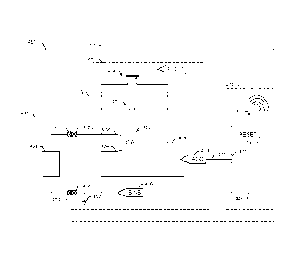
[0057] Figure 9 illustrates an example sensor signal 902, corresponding to
integrator output
signal 906, and corresponding interrupt signal 904 (with pulses 914a and 914b)
that may be
generated by an electronics assembly, such as electronics assembly 700 of
Figure 7. Figure 9
illustrates two stages of integration: a first stage that begins at time Ti
and a second stage that
begins at time T3. The first integration interval extends from time Ti to time
T2 and results in an
integrator output signal portion 908a. When the magnitude of the integrator
output signal reaches
the comparator threshold value 912 (less than the integrator circuit
saturation value of 910) at
time T2, the comparator provides an interrupt signal pulse 914a to a
processor, which triggers the
resetting of the integrator output signal. The second integration interval
extends from time T3 to
time T4 and results in an integrator output signal portion 908b. When the
magnitude of the
integrator output signal reaches comparator threshold value 912 at time T4,
the comparator
provides an interrupt signal pulse 914b to a processor, which again triggers
the resetting of the
integrator output signal. 1
[0058] In some embodiments, processor 748 may determine a value of the
integrator output
signal (per block 306 of Figure 3) by retrieving the known threshold value
from a memory or by
measuring the threshold value from threshold voltage source 736. Because
comparator circuit
17
CA 2933627 2017-05-11
744 provides an interrupt signal when the value of the integrator output
signal reaches the known
threshold value, processor 748 may determine an average value of the sensor
signal over the
integration interval in response to receiving the interrupt signal by
determining an elapsed time
between the first time and a time at which the interrupt signal is received at
the processor (e.g.,
the length of the integration interval). For example, in accordance with Eq. 3
above, the average
sensor current signal Is may be calculated as
THRESH x C
/s
(e)
where THRESH is the value of threshold voltage source 736, C is the
capacitance of capacitor
720, and T is the length of the integration interval.
[0059] Figure 10 is a plan view of an analyte sensor system 1000 that may
include any of the
sensor and/or electronics assemblies described herein (such as those described
with reference to
Figures 1, 4 and 7). A sensor assembly 1016 includes an analyte sensor 1010
configured to,
when sensor assembly 1016 is positioned against a body, produce a sensor
signal that is
representative of a level of an analyte in the body. Sensor assembly 1016 may
include, for
example, any of the sensor assemblies described herein. In some embodiments,
analyte sensor
1010 includes a sharp distal end 1010a configured to be positioned within the
body when the
sensor assembly 1016 is positioned against the body. In some embodiments,
analyte sensor 1010
includes a continuous glucose monitor.
[0060] A housing portion 1002 is coupled to sensor assembly 1016. An adhesive
pad 1012 is
disposed between housing portion 1002 and the body when in use, and a battery
1006 is disposed
within housing portion 1002. In some embodiments, battery 1006 is non-
rechargeable. In some
embodiments, battery 1006 is molded into housing portion 1002, and cannot be
removed. Battery
1006 may, for example, include one or more Li-Mn02 and/or silver oxide
batteries. In some
embodiments, housing portion 1002 is disposable when battery 1006 can no
longer provide
adequate power. In some embodiments, battery 1006 is a rechargeable battery,
or includes a
rechargeable battery.
18
CA 2933627 2017-05-11
[0061] Electronics assembly 1004 may take the form of any of the electronics
assemblies
described herein, such as electronics assembly 100 of Figure 1, electronics
assembly 400 of
Figure 4, and electronics assembly 700 of Figure 7. Electronics assembly 1004
may be
configured to perform any of the methods described herein, such as the method
of Figure 3, the
method of Figure 5, and the method of Figure 8. For example, in some
embodiments, electronics
assembly 1004 includes battery contacts 1008 configured to electrically couple
battery 1006 to
electronics assembly 1004 when electronics assembly 1004 is coupled to sensor
assembly 1016.
Electronics assembly 1004 may also include a sensor contact configured to
receive a sensor
signal from analyte sensor 1010, an integrator circuit coupled to the sensor
contact and
configured to provide an integrator output signal representative of the sensor
signal integrated
over time, a reset circuit coupled to the integrator circuit and configured to
reset the integrator
output signal in response to a reset signal, and a processor coupled to the
integrator circuit and
the reset circuit. The processor may be configured to determine a value of the
integrator output
signal and to provide the reset signal to the reset circuit when an
integration interval has elapsed
from the first time, the integration interval based at least in part on the
integrator output signal.
100621 Although certain embodiments have been illustrated and described
herein, it will be
appreciated by those of ordinary skill in the art that a wide variety of
alternate and/or equivalent
embodiments or implementations calculated to achieve the same purposes may be
substituted for
the embodiments shown and described without departing from the scope. Those
with skill in the
art will readily appreciate that embodiments may be implemented in a very wide
variety of ways.
This application is intended to cover any adaptations or variations of the
embodiments discussed
herein. Therefore, it is manifestly intended that embodiments be limited only
by the claims and
the equivalents thereof
19