Note: Descriptions are shown in the official language in which they were submitted.
CA 02934985 2016-06-30
Title: ONE AXIS SHUTTER WITH A PIN-BASED BUS SYSTEM FOR
MINIATURE CIRCUIT BREAKER LOAD CENTERS
FIELD OF THE INVENTION
[0001] The present disclosure relates to methods and systems for
inserting and removing a
circuit breaker from an electrical panel or panelboard, and more particularly
to a method and
apparatus for reducing the chances of exposure to live parts in the
panelboard.
BACKGROUND OF THE INVENTION
[0002] An electrical panel or panelboard, has a main bus and individual
connection points
on the bus that are connectable to electrical devices, such as circuit
breakers for branch
conductors and any other electrical devices designed to be installed for a
branch circuit.
Because the circuit breakers, sometimes referred to herein simply as
'breakers" for
convenience, and other branch electrical devices are typically mounted
directly to the
panelboard, an operator and/or tools may come in contact with exposed
conductors in the
panelboard when installing or removing the circuit breakers from the
panelboard. Thus, it is
recommended that power be shut off to the panelboard as a precaution when
electrical
devices are being installed or removed. However, it may be considered
desirable in some
cases to keep the panelboard energized to prevent an electrical hazard as a
consequence of
deenergization, or operators may intentionally keep the power on in the
interest of saving
time. Moreover, shutting off power to the panelboard can be a major
inconvenience,
especially for data centers, hospitals, and other critical applications that
require a high
availability power source.
[0003] Thus, a need exists for an improved way to safely insert and
remove a circuit
breaker or other switching equipment from an electrical panel as part of a
larger scheme for
installing and removing branch circuit devices without deenergizing the
electrical panel.
Measures to prevent unintentional contact with live, i.e. energized,
conductors are often
known as "finger safe" provisions. Work on energized equipment will be known
herein as
'live work". Particular panelboards, oftentimes called load centers, are front-
accessible, wall-
mounted panelboards, and typically for low voltage light, heat or power
circuit applications,
1
CA 02934985 2016-06-30
which have miniature circuit breakers to define and protect each branch
circuit. Due to their
size, design, and economic constraints, load center-type panel boards can
present unique
challenges for the above considerations.
SUMMARY OF THE DISCLOSED EMBODIMENTS
[0004] The embodiments disclosed herein are directed to methods and
systems for
reducing or eliminating the possibility of exposure to live parts in a
panelboard, and
particularly in the load center variety of panelboard, and safely installing
and removing a
circuit breaker or other branch electrical devices from the energized
panelboard. While the
illustrated embodiments are explained with load centers in mind, and the terms
"load center"
and "panelboard" may sometimes be used interchangeably herein, the present
invention is not
necessarily limited to the miniature circuit breaker load center environment.
[0005] The disclosed embodiments provide a shutter assembly for the
panelboard that
automatically closes off access to the conductors in the panelboard until a
circuit breaker is
inserted in the panelboard. A shutter assembly is attached in the circuit
breaker mounting
compartments, sometimes referred to herein as "wells," of the panelboard and
serves as one
part of a protective barrier for the busses of the panelboard. The circuit
breaker is designed
so that inserting it in the complementary panelboard in a Z-axis motion
unlocks and depresses
a shutter plate of the shutter assembly in a Z-axis motion and allows the
circuit breaker to
access the conductors in the panelboard, which also extend in the Z-axis. When
the circuit
breaker is removed from the panelboard, the shutter plate rises, locks and
again closes off
access to the conductors. Such a shutter assembly helps operators to safely
insert and remove
a circuit breaker or other electrical device from the panelboard while also
minimizing the
potential for exposure to live parts in the panelboard.
[0006] In some implementations, the shutter assembly comprises one moving
part which
is a perforate shutter plate with biasing towards the raised, or protective
position. One or
more springs at the sides of the shutter plate comprise a latching mechanism
holding the
shutter plate in the raised position in the absence of a circuit breaker
interacting therewith.
Thus the shutter assembly is robust and economical. The bus system of the
panelboard is laid
out to have power delivery and neutral return terminals, i.e. stabs, extended
in the Z axis so
that the stabs pass closely through the perforations of the shutter plate when
it is depressed by
an insertion of the breaker. The bus system of the load center beneath the
stabs is covered
2
CA 02934985 2016-06-30
with a nonconductive layer such as the bottom of a circuit breaker well
structure. Each stab
preferably sits beneath the top level of the shutter plate and is also capped
with a
nonconductive material to further prevent access to electrically live touch
points. The line
and neutral terminals of the complementary circuit breaker are female
receptacles in the
bottom of the breaker which cover and electrically connect to the bus stabs
upon insertion of
the breaker.
[0007]
Each branch circuit breaker slot of the load center is a compartment for a
circuit
breaker, desirably being a well-like structure with sides that extend in the Z
axis to
substantially cover the depth of the breaker when inserted to further minimize
access to live
conductors. The load side power and neutral connections for a branch circuit
are prewired
into the breaker interior before insertion of the breaker into the
compartment. These load side
connections extend from a side panel of the breaker through a slot in the
breaker
compartment leading to a wire gutter at the side of the load center. The wire
gutter may be
separately covered. The shutter plate will have the necessary length and width
to safely cover
the portion of the circuit breaker compartment conveying power and may include
a
mechanism that allows the shutter assembly to be firmly retained in the
breaker compartment
of the panelboard. The breakers are preferably equipped with positive
retention interlocks
providing a hold down mechanism and an interlock which will not allow the
breaker to be
inserted to, or removed from, the compartment in the ON position. Such
interlocks were
illustrated previously in Applicant's US patent Application serial no.
14/449,881 [CRC-
0298].
[0008]
Inserting the circuit breaker in the panelboard forces the shutter plate to
slide
from the raised, or protective, position into an lowered, or unprotected,
position where the
stabs extend through openings, i.e. throughholes, in the shutter plate aligned
therewith,
thereby allowing the female terminals of the circuit breaker to contact, i.e.
electrically
connect to, the male conductor stabs in the panelboard.
[0009]
In some implementations, the circuit breaker may have inclined planes on
portions
of an outer casing of the circuit breaker, for example, on the side walls
thereof. As the circuit
breaker is inserted in the panelboard, the inclined planes act as a keying
mechanism to line up
with latches holding the shutter plate in the protective raised position,
until the flat sides of
the breaker engage with and release the latches allowing the shutter plate to
be moved into
the lowered unprotected position. When the circuit breaker is removed from the
panelboard,
3
CA 02934985 2016-06-30
the shutter plate is forced upward by a biasing coil spring on the bottom side
thereof and the
latches, which are separate flat spring mechanisms, move back into the well to
latch the
shutter plate in the protective position.
[0010]
In one aspect, the disclosed embodiments are directed to a breaker compartment
in
a panelboard, and a shutter assembly in the breaker compartment, the shutter
assembly
disposed over the live conductor contacts and movable in one axis by a circuit
breaker
insertion in the same axis between a closed position in which the shutter
assembly blocks
access to the conductors of the panelboard and an open position in which the
shutter
assembly allows access to the conductors in the panelboard. Inserting a
circuit breaker in the
panelboard automatically puts the shutter assembly in the open position and
removing the
circuit breaker from the panelboard automatically puts the shutter assembly in
the closed
position.
[0011]
In another aspect, the disclosed embodiments are directed to an electrical
panelboard having a bus layout with pin-shaped stabs. Laid over the pin-shaped
stabs is a
circuit breaker compartment structure in the form of an open-faced box, with
the bottom
surface of the box, or an interstitial insulation layer, or both, covering all
the bus structure but
the stabs. The circuit breaker compartment structure provides individual
compartments for
the breakers and allows the stabs to protrude into the compai ________________
tinents; with each compartment
having a shutter assembly including a shutter plate with throughholes for the
stabs, a bias
spring urging the shutter plate to the closed position, and preferably a latch
for holding the
shutter plate to the raised protective position wherein access to the stabs is
closed off.
[0012]
In another aspect, the disclosed embodiments are directed to a panel board
assembly, including a power bus in a first plane with vertical stabs extending
90-degrees
from the power bus in a first axis; a neutral bus in the first plane with
vertical stabs extending
90-degrees from the neutral bus in the first axis; the stabs of each of the
power bus and the
neutral bus being arranged in a respective line; the stabs having a free end
being distal from
the busses, the free ends having caps of nonconductive material and extending
through a
nonconductive layer; circuit breaker compartments for receiving circuit
breakers inserted
along the first axis; the circuit breaker compai _____________________________
twents overlaying the nonconductive layer and
having the stabs protruding therein; a shutter plate in each of the circuit
breaker
compartments, each shutter plate having a throughhole for receiving a stab of
the power bus
and a throughhole for receiving a stab of the neutral bus; and the shutter
plate having a raised
4
position overlaying all pin-shaped stabs in a circuit breaker compartment and
having a
lowered position allowing the stabs of the circuit breaker compartment to
protrude
therethrough.
[0012a1 The following aspects are also disclosed herein:
1. A panel board assembly, including
a power bus in a first plane with vertical stabs extending 90-degrees from the
power
bus in a first axis;
a neutral bus in the first plane with vertical stabs extending 90-degrees from
the
neutral bus in the first axis;
the stabs of each of the power bus and the neutral bus being arranged in a
respective
line;
the stabs having a free end being distal from the power bus and the neutral
bus, the
free ends having caps of nonconductive material;
circuit breaker compartments for receiving circuit breakers inserted along the
first
axis; the circuit breaker compartments having the stabs protruding therein;
a shutter plate in each of the circuit breaker compai iments, each shutter
plate being
nonconductive and having a throughhole for receiving a stab of the power bus
and a
throughhole for receiving a stab of the neutral bus; and
the shutter plate having a raised position overlaying all stabs in its circuit
breaker
compartment and having a lowered position allowing the stabs to protrude
through the
shutter plate.
2. The panel board assembly of aspect 1, wherein the stabs are pin-shaped.
3. The panel board assembly of aspect 1, further comprising: a layer of
nonconductive
material covering the power bus and the neutral bus and allowing the stabs to
protrude
therethrough.
4. The panel board assembly of aspect 3, wherein the layer of nonconductive
material is a
nonconductive plate with throughholes for the stabs.
5. The panel board assembly of aspect 4, wherein the nonconductive plate is a
wall of a one-
piece unitary assembly of nonconductive material having the circuit breaker
compartments
formed therein.
6. The panel board assembly of aspect 1, further comprising: the shutter plate
being part of a
shutter assembly having a biasing spring for urging the shutter plate to the
raised position.
7. The panel board assembly of aspect 6 further having a latch for retaining
the shutter plate
in the raised position.
5
Date Regue/Date Received 2023-01-20
8. The panel board assembly of aspect 7, wherein the latch includes a U-shaped
flat spring
with tabs on arms of the U to engage the shutter plate.
9. The panel board assembly of aspect 8, wherein the arms of the U have a
first position
extending the tabs into contact with the shutter plate and a second position
upon contact with
a complementary-shaped circuit breaker wherein the tabs are forced towards
side walls of
circuit breaker compartment, thereby releasing the latch.
10. The panel board assembly of aspect 1, further comprising: the circuit
breaker
compartments each being a well whose sides extend in a Z axis to substantially
cover a depth
of the circuit breaker when inserted.
11. The panel board assembly of aspect 5, further comprising: a wiring gutter
in the one-
piece unitary assembly.
12. The panel board assembly of aspect 11, further comprising: a slot in the
circuit breaker
compartment on that side of the circuit breaker compartment leading to the
wiring gutter.
13. The panel board assembly of aspect 1, wherein the panel board is a load
center.
14. The panel board assembly of aspect 13, wherein the circuit breaker
compartments are
sized for miniature circuit breakers.
BRIEF DESCRIPTION OF THE DRAWINGS
[0013] The foregoing and other advantages of the disclosed embodiments
will become
apparent upon reading the following detailed description and upon reference to
the exemplary
explanatory drawings offered to illustrate the invention according to one or
more
embodiments disclosed herein, wherein:
[0014] FIGS. IA and 1B show top right perspective views of the circuit
breaker
compartment portions of an exemplary panelboard according to one or more
embodiments
disclosed herein, with descriptive axes of direction indicated thereon;
[0015] FIG. 2 shows a top perspective view of the well portions with
exemplary breakers
in four compartments and shutter assemblies in the bottom of the other
compartments;
[0016] FIGS. 3A and 3B show an exemplary uncovered and partially covered
bus layout,
respectively, for the load center;
[0017] FIG. 4 is a top perspective view similar to Fig. 2 showing exemplary
shutter
assemblies in the bottom of a circuit breaker compartment structure;
[0018] FIGS. 5A and 5B show details in perspective end view of circuit
breaker
compartments, two with partial cutaway; with shutter assemblies therein;
5a
Date Regue/Date Received 2023-01-20
[0019] FIG. 6 shows medial sectional perspectives through the Y-Z plane
of three
exemplary circuit breakers, breaker compartments and bus structure in
different stages of
engagement with the shutter assemblies; and
[0020] FIG. 7 shows a medial sectional perspective through the X-Z plane
of an
exemplary shutter assembly, a circuit breaker in engagement with the bus
structure; a deep
well circuit breaker compartment, and a wiring gutter.
DETAILED DESCRIPTION OF THE DISCLOSED EMBODIMENTS
[0021] As an initial matter, it will be appreciated that the development
of an actual, real
commercial application incorporating aspects of the disclosed embodiments will
require
many implementation specific decisions to achieve the developer's ultimate
goal for the
commercial embodiment. Such implementation specific decisions may include, and
likely
5b
Date Regue/Date Received 2023-01-20
CA 02934985 2016-06-30
are not limited to, compliance with system related, business related,
government related and
other constraints, which may vary by specific implementation, location and
from time to
time. While a developer's efforts might be complex and time consuming in an
absolute
sense, such efforts would nevertheless be a routine undertaking for those of
skill in this art
having the benefit of this disclosure.
[0022]
It should also be understood that the embodiments disclosed and taught herein
are
susceptible to numerous and various modifications and alternative forms. Thus,
the use of a
singular term, such as, but not limited to, "a" and the like, is not intended
as limiting of the
number of items. Similarly, any relational terms, such as, but not limited to,
"top,"
"bottom," "left," "right," "upper," "lower," "down," "up," "side," and the
like, used in the
written description are for clarity in specific reference to the drawings and
are not intended to
limit the scope of the invention.
[0023]
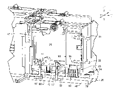
Referring now to FIGS. IA and 1B, a load center 21 is shown according to the
disclosed embodiments. It will be appreciated that various other covering and
enclosing
structure may form a finished version of the load center, including for
example a removable
wiring gutter cover 29 shown in Fig. 1B The load center 21 provides a
plurality of circuit
breaker compartments, collectively 23, in which circuit breakers, collectively
25, may be
mounted in order to connect to conductors, i.e. busses, collectively 27, in
the load center 21.
As shown, the circuit breaker compartments 23 can be formed in a one-piece
unitary
assembly 24 of nonconductive material in an overall box-shape having one open
side. The
one-piece unitary assembly 24 is fastened atop an insulative plate structure
26 having side
walls 28 spaced apart from the one-piece unitary assembly 24 and forming
wiring gutters 39.
[0024]
Fig. IA illustrates the required prewiring of the circuit breaker 25 prior to
insertion
in the panel board 21, with branch load line 31 and neutral line 33 being
inserted and
captured in the interior of the circuit breaker case and exiting through an
end panel 35 of the
circuit breaker 25. Fig. 1B illustrates the inserted circuit breaker 25 in its
compartment 23
with branch load and neutral lines 31, 33 respectively, exiting through a slot
37 in the end
wall 40 of the compartment which communicates with a wiring gutter 39.
[0025]
Fig. 2 shows a top perspective view of the circuit breaker compartment
portions
with exemplary breakers 25 in four respective circuit breaker compartments 23
and
nonconductive shutter plates, collectively 41, in the bottom of the other
circuit breaker
compartments. Three of the circuit breakers 25 are shown without branch wiring
for
6
CA 02934985 2016-06-30
simplicity. Visible in the two through-holes of each of the shutter plates 41
are the
nonconductive caps 43 covering the bus stabs. Also visible in Fig. 2 are the
receptacles 45
for the positive retention interlocks 47 of the circuit breakers 25.
[0026] As seen in Fig. 3A, the busses 27 of the load center are affixed
to a nonconductive
backplane 48 extending in the X-Y plane. The exemplary bus system is a three
phase power
bus system having an A phase 49, a B phase 51 a C phase 53, and two neutral
busses,
collectively 55, to accommodate a two row load center as better seen in Fig.
3B. Each bus
has a Y axis line of pin-shaped stabs, collectively 57, extending in the Z
axis, i.e. vertically.
Each stab 57 is capped with a nonconductive cap 43 at its free end, as
mentioned above.
Each bus 27 may extend beyond the backplane 48 for connection to incoming line
power. It
will be appreciated that various arrangements of the bus structure may be
possible dependent
upon factors such as the phases of power to be delivered through the load
center, etc. The
busses are then preferably covered with a nonconductive material, e.g. epoxy,
or the
insulative plate 26, which has been perforated with holes to allow the stabs
57 to protrude
therethrough into the circuit breaker compartments. It is envisioned that the
insulative plate
26 and unitary circuit breaker compartment structure 24 could be formed as a
single unit in
some aspects of the invention. The stabs 57 within the circuit breaker
compartments are then
covered with the shutter plates 41, such as seen in Fig. 2, such that the free
ends of the stabs,
preferably including the nonconductive caps 43, rest below the upper surface
of the shutter
plates 41 (Fig. 2) and within throughholes 58 (Fig. 4) of the shutter plates
so as to allow
access to the stabs when the shutter plates are depressed by circuit breaker
insertion.
[0027] As seen in the embodiment of Fig. 4, the shutter plate 41 need
not cover the entire
bottom of the circuit breaker compartment, but only such portion as is
necessary to protect
the load power and neutral stabs. For instance, the bottom of each circuit
breaker
compartment may also contain a communications port 59 by which appropriately
equipped
circuit breakers may communicate various information, or receive DC power, or
both. As
shown, the shutter plates 41 may have extension tabs 65 which are accommodated
in races
within cross bars 61 and front walls 63 in the well structure to provide added
stability. Also
seen are the tops of the latches 67 which retain the shutter plates 41 in the
raised and
protected position until released by insertion of a corresponding circuit
breaker, as further
explained below.
7
[0028] Figs. 5A and 5B are partially cutaway compartment structures to
show further
details of the shutter assemblies with a shutter plate, collectively 41,
within the structure of
the circuit breaker compartments 23, (identified individually in Fig. 5B as
compaitinents 23a,
23b and 23c), and supported in the raised and protected position by latches 67
engaging the
shutter plates 41. The compartment structures are not attached to the busses
in these views so
the stabs 43 are not seen. The latches 67 are in the form of U-shaped flat
springs with the
curve of the U held in place by a section of the bottom plate 60 of the
nonconductive one-
piece unitary assembly 24. The upwardly extending arms of the U's have inward
facing tabs
69 upon which rest the bottom surface 71 of the nonconductive shutter plate
41. While
shown as three U-shaped springs in each compartment 23, it will be appreciated
that the
number and design of the latch elements may vary.
[0029] As seen in Fig. 5B, a coil spring 73 is placed between the bottom
surface 71 of the
shutter plate 41 and the bottom plate 60 of the circuit breaker compartment 23
to bias the
shutter plate 41 upwardly in the Z axis towards the raised and protected
position in which it is
latched. The latches 67 are pushed by shaped elements of the inserted breaker
case (Fig. 6) to
the side walls 77 of the circuit breaker compartment 23, thereby moving the
tabs 69 out from
under the lower surface 71 of the shutter plate 41 to unlatch the shutter
plate 41 and allow it
to move downwardly to the lowered and unprotected position (Figs. 6-7). The
shutter plate
41 may have cut outs 79 providing a space into which the latch arms and tabs
69 can be
accommodated when the shutter plate is descending.
[0030] Referring also to Fig. 6, cross sections of two circuit breakers
25a, 25b are shown
in the fully inserted position while a third 25c is shown in a partially
inserted position. The
lower edges 81 of each breaker 25 are inclined or beveled in order to
gradually force the
latches 67 towards side walls 77 until the flat sides 82 of the circuit
breakers above the
beveled lower edges 81 force the latches fully open allowing the shutter
plates to be forced
down by the bottom surfaces 83 of the circuit breakers 25.
[0031] As seen in Fig. 7 once the circuit breaker 25 is fully inserted
with a Z axis motion,
the shutter plate 41 is fully depressed in the Z axis to the bottom plate 60
of the circuit
breaker compartment structure 24 allowing the line terminal 91 and neutral
female terminal
93 inside the bottom surface 83 of the circuit breaker 25 to make electrical
contact with the
vertical bus stabs 57. Appropriate shaping of the bottom surfaces of the
circuit breaker and
the top surfaces of the shutter plate, such as best seen in Fig. 7 may be
accomplished in the
design. As discussed above, the previously attached branch load and neutral
wires 31, 33 exit
8
Date Regue/Date Received 2023-01-20
CA 02934985 2016-06-30
the circuit breaker compartment 23 through slot 37 (Fig. 1B) into the wiring
gutter 39. The
communication port 59 of the circuit breaker compartment 23 has accepted the
corresponding
connector 95 on the circuit breaker 25 outside of the shutter plate area. The
positive retention
interlock 47 has been fastened, securing the circuit breaker in the circuit
breaker compartment
23 and allowing it to be placed in the ON position.
[0032] While particular aspects, implementations, and applications of
the present
disclosure have been illustrated and described, it is to be understood that
the present
disclosure is not limited to the precise construction and compositions
disclosed herein and
that various modifications, changes, and variations may be apparent from the
foregoing
descriptions without departing from the scope of the disclosed embodiments as
defined in the
appended claims.
9