Note: Descriptions are shown in the official language in which they were submitted.
CA 02935427 2016-06-29
Manufacture of a security element having color-change properties
[00011 This invention relates to a method for manufacturing a security
element
and to a security element and a value document containing said security
element.
[0002] Value documents as intended by the invention are, inter alia, bank
notes, shares, bonds, deeds, vouchers, checks, air tickets, high-value
admission
tickets, labels for product authentication, credit cards or cash cards, but
also other
documents at risk of forgery, such as passports, identification cards or other
identity documents.
[0003] Value documents, in particular bank notes, are usually produced from
paper substrates, polymer substrates or combinations of paper and polymer
which
have particular security features, such as a security thread at least partly
incorporated into the paper or a watermark. As further security features, so-
called
window foils, security threads, security bands can be bonded/laminated to the
value document or incorporated therein. Security elements usually comprise a
polymer or polymer compositions as a carrier material or base material.
Typically,
security elements have optically variable security features such as holograms
or
certain color-shift effects to thereby guarantee better anti-forgery security.
The
particular advantage of optically variable security elements is that the
security
features on said security elements cannot be imitated by mere copying using a
copying machine, since effects of an optically variable security feature are
lost or
even only appear black through copying.
100041 In existing value documents with optically variable security
elements
having color-shift effects, however, it is disadvantageous that the
manufacture of
the required thin-film elements is very time-consuming and cost-intensive. For
example, when manufacturing a thin-film element by means of physical vapor
deposition, in particular the manufacture of the necessary spacer layer is
very
time-consuming. For a definition and functionality of thin-film elements,
1
reference is made by way of example to the prints WO 2009/149831 A2 and WO
2011/032665 Al.
[0005] Further, the incorporation of additional security features such as
so-
called negative patterns or negative text in the region of the color-shift
effects/thin-film elements is elaborate and can frequently not be done with
satisfactory quality. For example, incorporating negative patterns into a
region
with a color-shift effect requires that the layers of the thin-film element
that lead
to the color-shift effect must be removed at least partly at the places where
the
negative patterns are to be incorporated.
[0006] It is hence an object of the present invention to provide a method
that
enables security elements having optically variable effects to be manufactured
in a
less time-consuming and cost-intensive manner.
[0007] It is likewise an object of the present invention to provide a
method that
enables security elements having optically variable effects and additional
negative
patterns to be manufactured in high quality.
[00081
[0009] A first aspect of the invention relates to a method for
manufacturing a
security element comprising the steps of:
- supplying a carrier material having at least one region to be coated;
- arranging a reflective layer in the region to be coated;
- arranging a structured spacer layer at the reflective layer, wherein the
structured spacer layer is adapted to protect the reflective layer from a
removing;
- arranging an absorber layer at least at the structured spacer layer; and
- removing the reflective layer in the regions where the removing of the
reflective layer is not prevented by the protection of the structured spacer
layer.
2
CA 2935427 2017-09-27
CA 02935427 2016-06-29
100101 The carrier material can have one or a plurality of regions to be
coated.
A carrier material preferably comprises two principal faces which stand or lie
opposite each other. The carrier material is preferably a foil-like material.
The at
least one region to be coated is preferably arranged at a principal face of
the
carrier material. When the carrier material has a plurality of regions to be
coated,
they can be arranged only at one of the two principal faces or at both
principal
faces of the carrier material.
100111 The carrier material's region to be coated can have different areal
shapes. For example, the region to be coated can be of rectangular, oval, star-
shaped or wiggly configuration. The shape and size of the region to be coated
is
preferably defined or determined in a method step. The carrier material's
region to
be coated can have a surface structure and/or surface condition that differs
from
other regions of the carrier material. The carrier material has, in other
words, an
area that is defined as a region to be coated.
100121 The step of "arranging a reflective layer in the region to be
coated"
preferably comprises that the reflective layer is arranged or applied on or
at/above
the area of the carrier material that is defined as a region to be coated.
100131 Preferably, the reflective layer is arranged or applied in the
region to be
coated over the full area. Preferably, the reflective layer can also be
arranged in
regions other than that to be coated. The reflective layer can for example be
applied or vapor-deposited by means of physical vapor deposition. Further
preferably, the reflective layer can also be applied by printing technology.
The
thickness of the reflective layer preferably lies in the range of 5 nm to 200
nm,
preferably 5 nm to 100 nm, particularly preferably 5 nm to 50 nm.
100141 Preferably, the step of "arranging a structured spacer layer at the
reflective layer, wherein the structured spacer layer is adapted to protect
the
reflective layer from a removing" is to be understood such that the reflective
layer
3
CA 02935427 2016-06-29
is arranged substantially between the carrier material and the structured
spacer
layer after the arranging of the structured spacer layer.
10015] A structured spacer layer is to be understood in particular to mean
that
the spacer layer is not arranged at/above the reflective layer uniformly or
over the
full area. In other words, after an arranging a structured spacer layer does
not have
the same layer thickness or layer height at every place of the region to be
coated.
Rather, due to the structured spacer layer there are places/subregions the
region to
be coated where the layer thickness of the structured spacer layer is zero.
[0016] After the arranging of the structured spacer layer at the reflective
layer
there are two different regions or portions in the region to be coated, namely
- first regions/portions comprising the carrier material, the reflective
layer and
the structured spacer layer, and
- second regions/portions comprising the carrier material and the
reflective
layer but no structured spacer layer or a structured spacer layer with a layer
thickness that is too small, so that the reflective layer is not protected by
the
structured spacer layer in said second regions. In other words, in this case
the
reflective layer is covered by the structured spacer layer only regionally or
they are arranged one over the other only in some subregions of the region to
be coated.
[0017] The structured spacer layer is adapted to protect the reflective
layer
from a removing. In other words, the structuring of the structured spacer
layer pre-
specifies in which (sub-)regions of the region to be coated the reflective
layer can
be removed/detached/dissolved/ablated. The structured spacer layer therefore
serves as a mask to enable a selective removing of the reflective layer.
[0018] Advantageously, the reflective layer can hence only be detached
where
the structured spacer layer was not arranged or undershoots a minimum layer
thickness or layer height. Therefore, the reflective layer is protected in
selected or
4
CA 02935427 2016-06-29
certain (sub-)regions in the region to be coated from a removing due to the
structure of the structured spacer layer.
[0019] Preferably, the structured spacer layer forms a predetermined motif
or
pattern such as a character, a character string and/or an image. Said motif or
pattern determines the structure of the structured spacer layer. The motif can
for
example be visible or recognizable to a viewer when the viewer looks in the
direction of the principal face normal or perpendicularly to the carrier
material's
principal face having the region to be coated.
100201 The step of "arranging an absorber layer at least at the structured
spacer
layer" is to be understood such that the absorber layer is in any case
arranged
at/above the structured spacer layer.
[0021] In one embodiment example, the absorber layer can additionally be
arranged at the regions of the reflective layer and/or of the carrier material
that are
not protected by the structured spacer layer. In other words, in this case the
absorber layer is arranged in the region to be coated over the full area.
[0022] The step of "removing the reflective layer in the regions where the
removing of the reflective layer is not prevented by the protection of the
structured
spacer layer" comprises in particular the cases of:
removing the reflective layer in the (sub-)regions where the structured spacer
layer is not arranged;
- removing the reflective layer in the (sub-)regions of the reflective
layer that
are not covered by the structured spacer layer;
- removing the reflective layer in the (sub-)regions where the structured
spacer
layer undershoots a minimum layer thickness, so that in said
subregions/regions no protection from a removing is given by the structured
spacer layer.
100231 In other words, the reflective layer is not removed where the
structured
spacer layer acts as a mask.
CA 02935427 2016-06-29
[0024] Advantageously, the structure of the structured spacer layer pre-
specifies in which (sub-)regions of the area that defines the region to be
coated the
reflective layer can be removed. Therefore, the reflective layer can be
removed
selectively, although the means employed for removing is applied over the full
area or not selectively in the region to be coated. For example, the means
employed for removing can be a laser beam with a planar cross section (e.g. l
cm2), wherein the entire region to be coated is treated with the laser steel
but a
removing of the reflective layer is possible only in the fields/(sub-)regions
not
protected by the structure of the structured spacer layer.
100251 If for example an etching means is employed for removing the
reflective layer, the security element can be completely dipped into the
etching
means or brought in contact with the etching means, wherein due to the
structure
of the structured spacer layer a removing of the reflective layer can only
take place
where the (predetermined) structure of the structured spacer layer does not
prevent/allows the removing.
[0026] In other words, the structured spacer layer serves as an etching
mask or
exposure mask.
[0027] Accordingly, after a removing of the reflective layer in the regions
where the removing of the reflective layer is not prevented by the protection
of the
structured spacer layer, the following regions are present:
regions containing the reflective layer, the structured spacer layer and the
absorber layer; said regions can also be designated thin-film-element
regions; and
regions containing no reflective layer and no spacer layer; said regions can
also be designated negative-pattern regions.
[0028] In particular, the layer sequence of reflective layer, structured
spacer
layer and absorber layer, wherein the structured spacer layer is arranged
between
reflective layer and absorber layer, forms a thin-film construction with a
color-
6
CA 02935427 2016-06-29
shift effect or a thin-film element with a color-shift effect. In dependence
on the
layer thicknesses of the reflective layer, the structured spacer layer and the
absorber layer, transmission-view color effects can also be present instead of
color-shift effects.
[0029] Preferably, the step of "arranging an absorber layer..." is
performed
(temporally) before the step of "removing the reflective layer...".
[0030] Preferably, in this embodiment the absorber layer is arranged both
at
the structured spacer layer and at (sub-)regions/partial regions of the
reflective
layer. In other words, in (sub-)regions of the region to be coated there are
so-
called second regions/second portions where the absorber layer is arranged
directly at the reflective layer. Consequently, in this case the removing of
the
reflective layer causes the absorber layer to be removed in the (sub-)regions
where
the structured spacer layer was not arranged. In other words, in said
subregions
there is no reflective layer, no spacer layer and no absorber layer. Said
subregions
are negative-pattern regions. Subregions containing a reflective layer, a
spacer
layer and an absorber layer are thin-film-element regions.
[0031] Advantageously, the reflective layer can be removed where the
absorber layer is arranged directly at the reflective layer when the absorber
layer is
transmissive to the removing means such as irradiation and/or etching means.
Preferably, the absorber layer is porous or holey, so that the absorber layer
does
not form a barrier for the removing means.
[0032] Simultaneous removing of the absorber layer and the reflective layer
in
only one method step is especially advantageous, since this enables the
manufacturing time and the manufacturing expense of security elements with a
color-shift effect or thin-film elements additionally containing negative
patterns to
be drastically reduced.
7
CA 02935427 2016-06-29
[0033] Preferably, the absorber layer has a thickness/height of 2 nm to 15
nm,
since the transmissivity of the absorber layer for a removing of the
reflective layer
is influenced by the thickness of the absorber layer.
[0034] Particularly preferably, the method for manufacturing a security
element comprises the steps of:
- supplying a carrier material having at least one region to be coated:
- arranging a reflective layer in the region to be coated over the full
area;
- arranging a structured spacer layer at/on the reflective layer, wherein
the
structured spacer layer is adapted to protect the reflective layer from a
removing;
- arranging an absorber layer in the region to be coated over the full
area;
- simultaneously removing the reflective layer and the absorber layer in
the
regions where the removing of the reflective layer is not prevented by the
protection of the structured spacer layer.
100351 Arranging an absorber layer in the region to be coated over the full
area
is effected such that the structured spacer layer is arranged between the
absorber
layer and the reflective layer, and in the regions where the structured spacer
layer
is not present the absorber layer is arranged directly at the reflective
layer.
[0036] It is especially advantageous that the reflective layer and the
absorber
layer can be applied/arranged in the region to be coated over the full area
and can
nevertheless be removed regionally in a targeted manner by a single "removing"
method step. It is also advantageous that the reflective layer and the
absorber layer
are not removed in the "removing" method step in the regions where the
structured
spacer layer is present. Advantageously, the absorber layer is porous or
transmissive to a corresponding removing means, so that the reflective layer
is
detached or dissolved in the regions where the reflective layer borders
directly on
the absorber layer. Due to the detachment or dissolution of the reflective
layer, the
absorber layer at the same time loses adhesion and is removed together with
the
reflective layer. In contrast, in the regions where the structured spacer
layer lies
8
CA 02935427 2016-06-29
between the absorber layer and the reflective layer the reflective layer is
protected
by the structured spacer layer. Although the absorber layer is also
transmissive to a
corresponding removing means in said regions, the structured absorber layer is
not
attacked by the corresponding removing means.
10037] According to an example, the absorber layer chosen can be chromium,
the structured spacer layer chosen can be a printing ink with good flow, for
example based on nitrocellulose, the reflective layer chosen can be aluminum.
As
an etching means there can in this case be employed for example caustic sodium
or phosphoric acid, which penetrates the chromium and dissolves the aluminum,
while the binder or printing ink for the structured spacer layer is not
impaired.
[0038] In particular, the absorber layer and/or the reflective layer can be
applied by printing technology.
[0039] Alternatively, the step of removing the reflective layer is
preferably
performed (temporally) before the step of arranging the absorber layer.
[0040] Preferably, the absorber layer is arranged in this alternative only
in the
(sub-)regions where the structured spacer layer is present. In other words,
the
absorber layer is preferably arranged exclusively at the structured spacer
layer.
[0041] Preferably, there thus arise (sub-)regions where no reflective
layer, no
structured spacer layer and no absorber layer are present (negative-pattern
regions), which are arranged beside other (sub-)regions where the reflective
layer,
the structured spacer layer and the absorber layer are present (thin-film-
element
regions).
[0042] Arranging the absorbers layer is preferably effected employing a
donor
foil. Preferably, the donor foil can be a metal donor foil. The absorber layer
can be
arranged at the structured spacer layer e.g. with a roll-to-roll method or be
transferred to the structured spacer layer by the donor foil.
9
CA 02935427 2016-06-29
100431 Further preferably, the method comprises the further step of
"arranging
a relief structure having elevated and recessed regions in the carrier
material's
region to be coated".
100441 When the relief structure is configured for example as a sine
grating or
crossed sine grating, the elevated regions lie where thc underlying
(normalized)
sine function assumes the value 1 or has a values range of 1 to greater than
0. 'the
recessed regions then lie for example at the value -1 or in the values range
of -1 to
smaller than 0.
[0045] Preferably, the relief structure is configured as an emboss
structure.
Preferably, the carrier material can have an emboss structure. Alternatively
or
additionally, there can be arranged at a principal face of the carrier
material at
least in the region to be coated a relief layer, preferably of emboss lacquer,
which
is furnished with a relief structure/emboss structure. Preferably, the method
can in
this regard have the following step sequence:
a) supplying a carrier material having at least one region to be coated/one
area
defined as a region to be coated;
b) arranging a relief structure in the region to be coated;
c) arranging a reflective layer at the relief structure in the region to be
coated.
[0046] Alternatively or additionally, a relief structure can be arranged
after the
arranging of the reflective layer, so that both the reflective layer and the
emboss
layer and/or the carrier material are furnished with a relief structure.
[0047] Further alternatively or additionally, a relief structure can be
arranged
after the arranging of the structured spacer layer, so that the relief
structure is
incorporated into the structured spacer layer.
[0048] Further alternatively or additionally, a relief structure can be
arranged
after the arranging of the absorber layer, so that the absorber layer itself
and/or a
(protective) layer covering the absorber layer have the relief structure.
CA 02935427 2016-06-29
[0049] Preferably, the method comprises the further step of "flattening out
the
relief structure by arranging the structured spacer layer at the reflective
layer".
[0050] Preferably, the recessed regions of the relief structure are filled
with
material of the structured spacer layer, so that the material of the
structured spacer
layer reaches at least the level of the elevated regions. Preferably, the
material of
the structured spacer layer is a liquid. Preferably, the relief structure is
scraped off
or drawn off/wiped off after an arranging/applying of the material of the
structured spacer layer, so that the material of the structured spacer layer
does not
exceed, or only slightly exceeds, the level of the elevated regions. The term
"slightly exceed" is to be understood in particular as a layer
thickness/height
exceeding the layer thickness/height up to the level of the elevated regions
by up
to 10%, preferably by up to 5%, of the layer thickness.
[0051] Advantageously, the drawing off/scraping off or wiping off of the
relief
structure after the applying of the material of the structured spacer layer
causes
excess material of the structured spacer layer to be removed. Consequently,
material of the structured spacer layer can thus be saved in the course of the
method/in the manufacturing process.
100521 After the arranging at the relief structure, the structured spacer
layer
has (sub-)regions with a higher layer thickness/height and therebeside (sub-
)regions with a lower layer thickness/height.
[0053] Preferably, the region to be coated has subregions having a layer
thickness of the structured spacer layer of zero or slightly thicker than
zero. In
other words, the structured spacer layer has a structure that corresponds
substantially to a negative of the relief structure.
[0054] Further preferably, the method comprises the further step of
"removing
the reflective layer in the elevated regions of the relief structure".
11
CA 02935427 2016-06-29
[0055] The structured spacer layer enables a removing of the reflective
layer
only in the (sub-)regions where the elevated regions are not, or only
slightly,
covered by the structured spacer layer or the level of the structured spacer
layer
does not exceed, or only slightly exceeds, the level of the elevated regions.
[0056] In other words, the reflective layer is removed in the regions where
the
reflective layer is not protected by the structured spacer layer.
[0057] When the level of the structured spacer layer is higher than that of
the
elevated regions, the structured spacer layer is first removed and then the
reflective layer. Advantageously, the reflective layer is retained in the
recessed
regions of the relief structure after the end of the step of "removing the
reflective
structure in the elevated regions of the relief structure", since the
structured spacer
layer is not, or not completely, removed during the method step, and hence the
reflective layer remains protected in the recessed regions.
[0058] Advantageously, the duration of a downstream step of "removing the
reflective layer in the elevated regions of the relief structure" will be kept
as short
as possible by restricting the layer thickness of the structured spacer layer
to a
maximum measure/maximum, since then the desired or fixed removing of the
reflective layer in the elevated regions of the relief structure is not
delayed by a
previously necessary removing of the structured spacer layer.
[0059] After a removing of the reflective layer in the elevated regions of
the
relief structure, an uneven surface structure may possibly be present. In
other
words, a relief structure can at least partly be present again. Hence, the
method
preferably comprises the further step of "flattening out the surface structure
in the
region to be coated" by
- arranging material of the structured spacer layer; and/or
- arranging filler.
[0060] Preferably, the filler or the filling material has a solids content
of
100%.
12
CA 02935427 2016-06-29
[0061] Preferably, the structured spacer layer is arranged/applied in the
form
of a motif by printing technology.
100621 Preferably, the structured spacer layer is arranged by means of one
or a
plurality of rollers and/or cylinders. In particular, the number of rollers
can vary.
The rollers/cylinders can transport lacquer and/or ink depending on the mutual
speed. The arrangement of the motif, or the motif printing, is preferably
effected
by a letterpress form.
[0063] Preferably, the structured spacer layer is applied by means of
tlexographic printing. Alternatively or additionally, the structured spacer
layer is
applied by means of gravure printing. Alternatively or additionally, the
structured
spacer layer is applied by means of ink-jet printing. Alternatively or
additionally,
the structured spacer layer is applied by means of offset printing.
Alternatively or
additionally, the structured spacer layer is applied by means of screen
printing.
Alternatively or additionally, the structured spacer layer is arranged by
means of
3D printing.
[0064] Preferably, the print unit for arranging the structured spacer layer
can
be encapsulated or atmospherically sealed, so that an atmosphere saturated
with
solvent is present in the print-unit region. Advantageously, the solvent-
saturated
atmosphere prevents/avoids a drying up of the printing ink or of the
dielectric on
rollers and/or cylinders.
[0065] Advantageously, by means of an arrangement/application of the
structured spacer layer by printing technology one can achieve the desired
layer
thickness very fast for example in comparison to an application by means of
physical vapor deposition. Further advantageously, upon an application by
printing technology one can already achieve the structure or structuring of
the
structured spacer layer very simply upon the arranging, so that after an
arrangement of a spacer layer there is no need for a further/downstream method
step for structuring such a spacer layer. In contrast, upon the arranging of a
spacer
13
CA 02935427 2016-06-29
layer by means of physical vapor deposition, for example, there is usually
applied
a full-area/uniform or unstructured spacer layer which is then removed
regionally
e.g. by means of an etching operation to thereby obtain a structured spacer
layer.
[0066] Preferably, the step of "removing the reflective layer..." comprises
etching.
[0067] In other words, the reflective layer is removed by means of an
etching
operation or etching means as a removing means. Preferably, the etching means
employed is caustic sodium or phosphoric acid.
[0068] Advantageously, the etching means penetrates the absorber layer, so
as
to establish a contact between etching means and reflective layer.
Advantageously,
the reflective layer can therefore be dissolved or detached. Advantageously,
the
detaching of the reflective layer likewise undoes the firm bond/connection
between the absorber layer and the carrier layer. so that the removing of the
reflective layer at the same time removes the absorber layer. In the (sub-
)regions
where the structured spacer layer is arranged, the etching means can
advantageously not contact the reflective layer after a penetrating of the
absorber
layer, so that the reflective layer and the absorber layer remain in place in
said
regions.
[0069] Alternatively or additionally, the step of "removing the reflective
layer..." comprises lasering.
[0070] In other words, the reflective layer is removed by means of a laser-
beam treatment as a removing means. Further preferably, the absorber layer is
not
detached or impaired by the laser radiation. Advantageously, the laser
radiation
can penetrate the absorber layer and remove the reflective layer.
Advantageously,
the structured spacer layer protects the reflective layer sufficiently from
the laser
radiation, so that the reflective layer is not removed in the (sub-)regions
where the
structured spacer layer is arranged.
14
CA 02935427 2016-06-29
[0071] For example, the employed laser can emit infrared laser radiation,
and
the structured spacer layer have infrared-blocking properties, so that the
laser
radiation cannot penetrate the structured spacer layer.
[0072] Preferably, the method comprises the further step of "arranging an
adhesion-promoting layer".
[0073] Preferably, the adhesion-promoting layer is arranged (temporally)
before the step of "arranging the reflective layer...". In other words, the
adhesion-
promoting layer is arranged between the carrier material and the reflective
layer.
Advantageously, the bond or connection between the reflective layer and the
carrier material is improved by the adhesion-promoting layer. When an emboss
lacquer/emboss-lacquer layer is arranged between the carrier material and the
reflective layer, the adhesion-promoting layer improves the bond of the
carrier
material and the reflective layer. The adhesion-promoting layer can comprise
metallic and/or non-metallic materials.
[0074] Alternatively or additionally, the method comprises the further step
of
"applying a protective layer".
100751 Advantageously, the protective layer is arranged after "arranging
the
absorber layer..." or "removing the reflective layer..." in order to protect
the
structures produced by means of the method. Advantageously, the protective
layer
is arranged in the (entire) region to be coated.
[0076] Preferably, the protective layer comprises a protective lacquer.
Alternatively or additionally, the protective layer comprises a heat-seal
lacquer
and/or a primer.
100771 Preferably, the structured spacer layer has at least partly
deformation
properties which lead to deformation-induced color changes of the security
element.
CA 02935427 2016-06-29
[0078] This makes a color change recognizable to a viewer in the deformed
portions of the region to be coated in comparison to a non-deformed state
after a
deforming of the structured spacer layer.
[0079] Advantageously, the deformation of the structured spacer layer leads
to
a (regional) color change of the security element or of the region to be
coated in
the deformed portions where the structured spacer layer has the deformation
properties which lead to deformation-induced color-change properties of the
security element.
[0080] Preferably, such a color change of the security element or the
deformation of the structured spacer layer is reversible. Advantageously, the
color
change persists at least for some time after the deformation, so that the
color
change is still recognizable to a viewer for a while in a state that is no
longer
deformed.
[0081] Advantageously, after an arranging of the structured spacer layer
the
deformation-induced color-change properties can be adjusted or fixed. The
deformation-induced color-change properties can be fixed by thermal cross-
linking and/or vulcanization and/or radiation curing.
[0082] According to one embodiment, the entire structured spacer layer has
deformation properties which lead to deformation-induced color-change
properties
of the security element. According to a further embodiment, only partial
regions/portions of the structured spacer layer have deformation properties
which
lead to deformation-induced color-change properties of the region to be coated
or
of the security element. For example, the partial regions/portions of the
structured
spacer layer that arc to have deformation properties for a color change can be
defined or fixed by means of selective irradiation.
[0083] Preferably, it is fixable by means of a mask which portions of the
security element or of the region to be coated are to have deformation-induced
color-change properties. In other words, a mask is employed to furnish a
16
CA 02935427 2016-06-29
structured spacer layer with portions having deformation properties for
deformation-induced color changes of the security element.
100841 Preferably, the mask protects the portions of the structured spacer
layer
that are to have or not to have deformation-induced color-change properties
from
an irradiation/vulcanization or thermal cross-linking.
100851 Preferably, such a mask is configured as a motif or pattern.
Consequently, it is possible that upon or after a deforming of the region to
he
coated a (further) pattern/motif is/becomes recognizable to a viewer due to
the
color change in the portions of the region to be coated with deformation-
induced
color-change properties.
100861 Preferably, a structured spacer layer having deformation properties
hich lead to deformation-induced color changes of the security element is of
gel-
like configuration at least in some portions. Preferably, the structured
spacer layer
is an elastomer. For example, bending or folding a security element having a
structured spacer layer that is of gel-like or jelly-like configuration at
least in some
portions can cause a local change in the layer thickness of the structured
spacer
layer of gel-like configuration, so that said local layer-thickness change in
the
thin-film-element region reveals a color change of said thin-film-element
region
upon viewing of the security element.
[0087] Alternatively or additionally, deformation properties of the
structured
spacer layer which lead to a recognizable color change can be achieved by a
swelling behavior differing at least in some portions. For example, this can
cause a
color change to become recognizable to a viewer, upon moistening of the
security
element, in the portions of the structured spacer layer having a stronger
swelling
behavior in comparison to the portions of the structured spacer layer having a
lesser swelling behavior. Advantageously, the color change persists at least
for
some time after the swelling, so that the color change is still recognizable
to a
17
CA 02935427 2016-06-29
viewer after a moistening, for example after he has breathed on it and thereby
caused a swelling.
100881 According to a further embodiment, the entire structured spacer
layer
has a strong swelling behavior, so that after a moistening a color change is
recognizable upon viewing of the security element due to a layer-thickness
increase of the structured spacer layer brought about by swelling.
[0089] Preferably, the structured spacer layer has direction-dependent
refractive indices.
[0090] In other words, the structured spacer layer is an anisotropic layer.
Advantageously, a viewer can recognize a different color-shift effect
depending
on the direction of viewing the region to be coated or the security element
due to
the direction-dependent refractive indices. For example, a (further) color-
shift
effect can be recognizable upon viewing the region to be coated from an
oblique
direction and turning/rotating the region to be coated around the principal-
face
normal in the centroid of the region to be coated. Preferably, said color-
shift effect
is different in color from the other color-shift effects in the region to be
coated.
[0091] Preferably, the structured spacer layer has one or a plurality of
colorants.
[0092] Preferably, the structured spacer layer has pigments. Preferably,
the
pigment size or pigment dimensions/diameter does not exceed the layer height
or
layer thickness of the structured spacer layer.
[0093] Preferably, the colorants and/or pigments comprise fluorescence
properties.
[0094] Advantageously, the structured spacer layer has a toning or slight
coloring, so that the structured spacer layer appears at least not completely
transparent to a viewer.
18
CA 02935427 2016-06-29
[0095] Advantageously, a fluorescing or a toning or a slight coloring of
the
structured spacer layer enables the structured spacer layer to be visible or
to be
made visible to personnel upon manufacture of the security element. This can
facilitate for example a check of the manufacturing process or of the method
step
of "arranging the structured spacer layer".
100961 Preferably, the structured spacer layer has a dry layer thickness of
30
nm to 1100 nm, preferably 300 nm to 600 nm. Preferably, there is recognizable
to
a viewer of the security element having a structured spacer layer with a dry
layer
thickness/height of less than 350 nm a motif, in a (single) color, which is
formed
by the structured spacer layer.
[0097] At a dry layer thickness of the structured spacer layer of 350 nm a
color-shift effect is recognizable to the viewer. At a dry layer thickness of
the
structured spacer layer of 30 nm to 80 nm no color-shift effect is
recognizable, but
rather a deep black.
(0098] Preferably, the security element has at least one relief structure
such as
a hologram and/or moth-eyes and/or microlenses and/or micromirrors.
[0099] Preferably, the relief structure can be provided with the step of
"arranging a relief structure having elevated and recessed regions in the
carrier
material's region to be coated". Alternatively or additionally, there can be
provided
other/further relief structures which are arranged in other layers such as the
emboss layer, the structured spacer layer, the absorber layer and/or the
protective
layer.
[0100] Preferably, the carrier material comprises a carrier foil.
Particularly
preferably, the carrier material contains polyethylene terephthalate (PET)
and/or
polypropylene (PP), the carrier material being particularly preferably made of
PET
or PP.
19
CA 02935427 2016-06-29
[0101] Preferably, the carrier material can be removed before the applying
of
the security element to a value-document substrate. Preferably, the security
element comprises at least one adhesive layer or at least one release layer
which is
applied between the carrier material and the reflective layer.
[0102] Preferably, the reflective layer contains aluminum and/or silver. In
particular, the reflective layer is an aluminum layer or a silver layer.
[0103] Preferably, the absorber layer contains a material transmissive to
an
etching means. Preferably, the absorber layer contains a material transparent
or
semi-transparent to laser radiation. In other words, the absorber layer
contains a
material at least semi-transparent to laser radiation. Preferably, the
absorber layer
contains chromium. In particular, the absorber layer is a chromium layer.
[0104] Preferably, the structured spacer layer is a dielectric. Preferably,
the
dielectric has resist-lacquer properties.
[0105] Preferably, the structured spacer layer is based on vinyl chloride
copolymers with acid groups. Vinyl chloride copolymers with acid groups may be
for example the product 1-1 15/45 M from Wacker Chemie AG, which is sold under
the trademark VINNOL . As specified by the manufacturer, H 15/45 M is a
carboxyl group-containing terpolymer of approx. 84 wt.% vinyl chloride (VC)
and
approx. 15 wt.% vinyl acetate (VAc) as well as approx. 1 wt.% dicarboxylic
acid.
According to the manufacturer, it is preferably used as a binder for lacquers
and
printing inks.
[0106] Preferably, the structured spacer layer is based on nitrocellulose.
This
achieves a good flow of the structured spacer layer.
[0107] Preferably, the structured spacer layer is based on acrylate(s).
This
enables a high transparency and later deformability through embossing or
stamping. Advantageously, the structured spacer layer contains an acrylate
flow-
control additive such as Byk 361. The latter can advantageously promote an
even
CA 02935427 2016-06-29
surface structure of the structured spacer layer, so that the absorber layer
can be
arranged on such an even surface structure. Preferably, the structured spacer
layer
is based on acrylic acid ester. Preferably, the structured spacer layer is
based on
epoxide(s). Preferably, the structured spacer layer is based on
polyurethane(s). The
advantage of epoxides and polyurethane(s) is a good cross-linkability, so that
a
good stability is obtained upon overprinting with solvent-containing lacquers.
Preferably, the structured spacer layer can also be based on combinations of
the
above substances. Further preferably, the structured spacer layer is based on
a
water-soluble substance. Preferably, the structured spacer layer can be based
on
vinyl chloride copolymer with acid groups (e.g. VMCH, which is a product name
of a vinyl chloride copolymer with acid groups and is manufactured by Dow
Chemical Company). A sample formulation could be for example as follows: 20%
vinyl chloride copolymer with acid groups (VMCH), 20% methyl ethyl ketone
(MEK), 20% ethyl acetate, 20% toluene, 20% butyl acetate. VMCH has a very
good adhesion on metals. The contained solvent mixture is well suited for
preventing drying artifacts. Polyvinyl butyral is likewise suitable. UV-
reactive
coatings can likewise be used.
[0108] According to one embodiment example, when an etchable layer (e.g.
aluminum) is applied as a reflector in the first step, for example, a
photoresist can
be applied even over the full area in a second step. Through an exposure there
can
be created washable/etchable and non-washable/non-etchable regions. Said
exposure can be effected before or also after the applying of the absorber.
When
the regions of the resist that have the corresponding sensitivity are now
removed
by washing/etching, the reflective layer can be structured either
simultaneously, or
in a following step with a further etching medium. In this procedure the
absorber
layer is structured as well, without having to be etched itself.
101091 Alternatively or additionally, the structured spacer layer comprises
nematic liquid crystals. Advantageously, there can be supplied by means of
21
CA 02935427 2016-06-29
nematic liquid crystals a structured spacer layer having direction-dependent
refractive indices.
101101 Preferably, nematic liquid crystals can be printed as a (structured)
spacer layer. Preferably, said nematic liquid crystals are aligned by suitable
arrangement/alignment methods, such as emboss arrangement, photo arrangement,
arrangement by shear upon printing or arrangement based on the choice of
substrate to be printed. When a spacer layer having such aligned nematic
liquid
crystals is supplied, further optically variable effects are obtained in
addition to
the color-shift effect based on the thin-film element. When the nematic liquid
crystals form a uniform, altogether anisotropic structured spacer layer, then
said
structured spacer layer has a (different) refractive index dependent on the
viewing
direction. Consequently, the color-shift effect varies in dependence on the
viewing
direction. An additional color change results for example upon oblique viewing
and horizontal rotation of the security element. When the nematic liquid
crystals
of the structured spacer layer are aligned regionally differently, the
regionally
differently aligned liquid crystals yield a (separate) motif. It can thereby
be
achieved that a uniform color is perceived upon nearly perpendicular viewing
of
the principal face of the security element, while the (separate) motif from
the
regionally differently aligned liquid crystals is/becomes recognizable upon
tilting
of the security element/oblique viewing of the principal face of the security
element.
[0111] Preferably the structured spacer layer does not consist of SiO2.
[0112] A further aspect relates to a security element, wherein the security
element has been manufactured by one or a plurality of the previously
described
method steps and/or from the described aspects.
[0113] A security element according to this invention can contain in
particular
a foil or a multilayer substrate, wherein the multilayer substrate can also
have a
combination of fabric substrates and foils. For example, the security element
can
22
CA 02935427 2016-06-29
comprise a window region which serves to fill, or bridge, a hole in a value
document or in the paper substrate of the value document. In other words, with
the
security element there can be incorporated/applied a security window in a
value
document. Preferably, the region to be coated is arranged in the window region
of
the security element. Alternatively, the security element can be applied to a
value
document, for example laminated or bonded thereto. The security element can be
a
security thread or security band, windowed thread, patch or the like.
101141 A further aspect relates to a value document, in particular a bank
note,
having a value-document substrate and at least one security element that has
been
manufactured by means of one or a plurality of the previously described method
steps and/or from the described aspects.
101151 A security element is preferably applied to/incorporated into a
value-
document substrate. A value-document substrate can have paper, polymer or a
paper-polymer combination. In the case of a bank note made of polymer or a
paper-polymer combination as a value-document substrate, the carrier material
of
the security element can be a partial region of the value-document substrate.
For
example, the value-document substrate can be a polymer foil and the carrier
material of the security element is a partial region of said polymer foil.
101161 When the security element has been embedded into a value document,
the upper side and the underside of the security element preferably extend
(substantially) parallel to the upper side and underside of the value-document
substrate. The upper side and underside of the value document as well as those
of
the security element can also be designated principal faces. Said principal
faces
render relevant information to a viewer. Consequently, the principal faces are
visible to a viewer viewing a value document having a security element. For
example, a principal face of a bank note can render the value of the bank note
as
well as its serial number. Accordingly, an upper side and underside of a
security
element, like those of a value document, can also be regarded as first and
second
principal faces.
23
CA 02935427 2016-06-29
[0117] The invention
will be explained hereinafter on the basis of preferred
embodiments in connection with the attached figures, whose representation does
without a true-to-proportion and true-to-scale rendition in order to increase
the
illustrative value.
101181 There are shown:
Figs. I a, lb a schematic representation of a value document having a security
element;
Figs. 2a-f a schematic
representation for the manufacturing method of a
security element according to a first variant:
Figs. 3a-e a schematic
representation for the manufacturing method of a
security element according to a second variant;
Figs. 4a-g a schematic
representation for the manufacturing method of a
security element according to a third variant;
Figs. 5a-5c a schematic sectional representation of security elements having a
protective layer;
Figs. 6a, 6b a schematic representation of a detail of a value document having
a
security element:
[0119] Figures la and
lb respectively show a schematic plan view of a
principal face of a value document 100 having a value-document substrate 102
and a security element 104, wherein the security element 104 is firmly
connected
to the value-document substrate 102, e.g. embedded into the value-document
substrate 102 or applied to the value-document substrate. The security element
104 can also be a partial region of the value-document substrate 102.
[0120] The security
element 104 has an area defined as a region 106 to be
coated, said area comprising a negative-pattern region 108 and a color-shift
or
thin-film-element region 110.
24
CA 02935427 2016-06-29
[0121] Figure la shows the number 45 as a negative-pattern region 108a.
while Figure lb shows three stripes as a negative-pattern region 108b.
[0122] A negative-pattern region can further have any form or
configuration.
For example, a negative-pattern region might have the form of a church or an
animal. Preferably, a negative-pattern region enables a viewer to recognize
the
negative-pattern region in plan view and/or in transmission view. Preferably,
the
security element is transparent or at least semi-transparent in the negative-
pattern
region, so that at least a portion of the light impinging on the security
element is
transmitted in the negative-pattern region. Further preferably, the negative-
pattern
region can have a different color appearance in plan view compared to
transmission view (so-called transmission-view color effects). In other words,
the
color appearance of the negative-pattern region in plan view (e.g. gold), by
which
the share of reflected light determines the color appearance, is different
from in
transmission view (e.g. blue), by which the share of transmitted light
determines
the color appearance. The security element 104 contains a carrier material
which
preferably consists of polyethylene terephthalate (PET), and has a region 106
to be
coated. The thin-film-element region 110, which is a subregion or partial
region of
the region 106 to be coated, comprises at least one reflective layer, a
structured
spacer layer and at least one absorber layer. In comparison to the thin-film-
element region 110, the negative-pattern region 108 has at least no reflective
layer
and no structured spacer layer.
[0123] Accordingly, it is clearly evident that the structured spacer layer
is not
present over the full area or uniformly in the region 106 to be coated, but
only/exclusively in the thin-film-element region 110.
[0124] The construction of a region 108 to be coated having thin-film-
element
region 110 and negative-pattern region 108 will be explained more closely
hereinafter with the aid of Figures 2 to 5.
CA 02935427 2016-06-29
[0125] Figs. 2a to 2f show different (method) steps for manufacturing a
security element having a thin-film-element region and a negative-pattern
region.
[0126] Fig. 2a shows the sectional view of a region 202 to be coated of a
carrier material 200. The region 202 to be coated is arranged at the principal
face
HF of the carrier material. For manufacturing a security element as it is
shown in a
comparable manner in Figures la and lb, the method step of "supplying a
carrier
material 200 having at least one region to be coated" is followed by a method
step
of arranging a reflective layer 204 in the region 202 to be coated. Fig. 2b
shows in
this connection a reflective layer 204 which was arranged in the region 202 to
be
coated. As is evident from Fig. 2b, the reflective layer 204 was arranged at
the
principal face HF of the carrier material. As is evident from Fig. 2b, the
reflective
layer 204 is arranged in the region 202 to be coated over the full area. In a
next
step, as shown in Fig. 2c, a structured spacer layer 206 is arranged at the
reflective
layer 204. Due to the structure of the structured spacer layer 206 there are
formed
in the region 202 to be coated a thin-film-element region 210 consisting of a
plurality of subregions 210a to 210c and a negative-pattern region 208
consisting
of the subregions 208a and 208b. For example, the structured spacer layer 210
corresponds to the thin-film-element region 110a or 110b according to Figures
la
and lb. Consequently, the negative-pattern region 208 can have a motif or a
form
like the negative-pattern regions 108a or 108b of Figures la and lb. In other
words, the structure of the structured spacer layer fixes which regions or
subregions of the region 202 to be coated are configured as thin-film-element
regions 210 or negative-pattern regions 208.
[0127] Advantageously, the structured spacer layer 206 is a dielectric.
Further
advantageously, the structured spacer layer 206 can be arranged at the
reflective
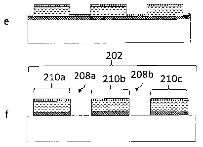
layer 204 by means of one or a plurality of rollers or printing methods. This
is in
particular advantageous, since it enables a great variety of structures or
motifs that
are to have the structured spacer layer 206 to be manufactured in a simple
manner.
26
CA 02935427 2016-06-29
[0128] In a further method step, an absorber layer 212 is arranged in the
region
202 to be coated, as shown in Fig. 2d. As is evident from Fig. 2d, the
absorber
layer 212 is arranged in the region 202 to be coated over the full area. In a
next
method step, as shown in Fig. 2e, the reflective layer 204 is removed in the
regions where the reflective layer 204 is not protected by the structured
spacer
layer 210. In other words, the structured spacer layer 206 serves as a mask or
protective layer, thereby enabling a selective removing of the reflective
layer 204.
For example, the removing of the reflective layer can be achieved, as shown in
Fig. 2e, by means of homogeneous irradiation or by employing an etching means
214. Advantageously, the removing of the reflective layer 204 causes the
absorber
layer 212 to be removed at the same time. This results in a security element
having
a region 202 to be coated, as represented in Fig. 2f. In particular, only the
thin-
film-element region 210 or the thin-film-element subregions 210a, 210b, 210c
have a reflective layer 204. In other words, the removing of the reflective
layer
204 in the regions 208a, 208b where the removing of the reflective layer 204
is not
prevented by the protection of the structured spacer layer 206 has given rise
to a
structured reflective layer and a structured absorber layer. Said structured
reflective layer and said structured absorber layer preferably have the same
structure/structuring as the structured spacer layer 206.
[0129] In particular, the sectional representation shown in Fig. 2f of a
region
202 to be coated can correspond to a section along the line I-I according to
Fig. 1 a
or the line II-II according to Fig. lb.
[0130] Figures 3a to 3e show the different method steps for manufacturing a
security element according to a further variant. Fig. 3a shows the supplying
of a
carrier material 300 having a principal face HF and a region 302 to be coated
in a
sectional view. Said sectional view can correspond for example to a sectional
view
along the line I-I as shown in Fig. la, or along the sectional line 11-11
according to
Fig. lb. Fig. 3b shows the method step of "arranging a reflective layer 304"
in the
region 302 to be coated. As already shown in Fig. 2b, the reflective layer 304
is
27
CA 02935427 2016-06-29
also arranged at the principal face HF in the region 302 to be coated over the
full
area or uniformly or in an unstructured manner. In a subsequent method step,
the
structured spacer layer 306 is arranged at the reflective layer 304. Due to
the
structure of the structured spacer layer 306 there result in the region 302 to
be
coated regions or subregions 310a - 310c having a structured spacer layer 306,
and
regions or subregions 308a, 308b in the region 302 to be coated which have no
structured spacer layer 306.
101311 The structured spacer layer 306 is adapted to protect the reflective
layer
304 from a removing. In a next method step, the reflective layer 304 is
removed in
the regions 308a, 308b. In other words, the structured spacer layer 306 serves
as a
mask or enables a selective removing of the reflective layer 304. Said
removing
can advantageously be performed by means of homogeneously applied removing
means, such as radiation or etching means, due to the function of the
structured
spacer layer 306 as a mask. A substantially homogeneous action of a removing
means or an irradiation or an etching means 314 is represented schematically
in
Fig. 3d. In a subsequent method step, an absorber layer 312 is arranged in the
region 310 or the subregions 310a, 310b, 310c. Consequently, there results a
negative-pattern region 308 or negative-pattern regions 308a, 308b where no
reflective layer 304 and no absorber layer 312 are arranged. In other words,
the
absorber layer 312 is applied selectively or in a structured manner in
accordance
with the structure of the structured spacer layer 306. Thus there arises, in
other
words, a structured absorber layer 312.
101321 Preferably, the manufacturing methods as set forth with reference to
Figures 2 and 3 can comprise further or additional method steps. In
particular,
such further or additional method steps can also be performed between one or a
plurality of the explained method steps. For example, there can be performed
as an
additional method step the arranging of a relief structure, wherein this
method step
is performed before an arranging of the reflective layer 204 or 304.
28
CA 02935427 2016-06-29
101331 A further variant for manufacturing a security element will now be
explained with reference to Figures 4a to 4f. Fig. 4a shows thc sectional view
of
a carrier material 400 having a principal face HF and a region 402 to be
coated.
The carrier material 400 having the region 402 to be coated is supplied within
the
context of a method step as shown in Fig. 4a. In a further method step, a
relief
structure 404 having elevated regions 408 and recessed regions 406 is arranged
in
the carrier material's 400 region 402 to be coated. According to one
embodiment,
the relief structure can be configured or shaped by embossing the carrier
material
400. According to another embodiment example, the relief structure 404 can be
arranged or shaped by a relief layer/emboss layer, such as an emboss lacquer,
being applied or arranged on the principal face FIF of the carrier material
and said
emboss layer being given a relief structure 404 by an embossing tool. In
particular,
a relief structure 404 can be arranged or formed by a relief structure 404
being
incorporated into a relief layer e.g. by means of etching or lasering. With a
further
method step, a reflective layer 410 is arranged in the region 402 to be
coated. This
can be effected for example by vapor deposition methods, so that material of
the
reflective layer 410 arranges itself or is applied in the elevated regions
408a-d and
in the recessed regions 406a-e. In this regard, reference is made to Fig. 4c.
In a
further method step, a structured spacer layer 412 can be arranged, as shown
in
Fig. 4d. In so doing, the structured spacer layer is arranged at least in the
recessed
regions 406a-e at the reflective layer 410. In other words, the relief
structure 404
is flattened out by arranging the structured spacer layer 412 at the
reflective layer
410.
[0134] Preferably, material of the structured spacer layer 412 is not
located, or
located only slightly, at the reflective layer 410 in the elevated regions
408a-d.
This can be attained for example by performing a scraping off or
detaching/wiping
off of excess material of the structured spacer layer 412.
[0135] The structured spacer layer 412 forms a protection or a mask, so
that
the reflective layer is protected from a removing in the recessed regions 406
29
CA 02935427 2016-06-29
during the method step of "removing the reflective layer 410 in the elevated
regions 408 of the relief structure 404". When a slight or thin layer of
material of
the structured spacer layer 412 is also located at the reflective layer 410 in
the
elevated regions 408, material of the structured spacer layer 412 is first
ablated
and thereafter the reflective layer 410 in the elevated regions 408 within the
context of the method step of "removing the reflective layer in the elevated
regions of the relief structure". The reflective layer 410 in the recessed
regions
406 still remains protected by the (remaining) structured spacer layer 412,
since
the method step of "removing the reflective layer in the elevated regions" is
ended
after the reflective layer 410 was removed in the elevated regions 408. This
is
shown for example with reference to Fig. 4e, wherein the reflective layer 410
was
removed in the elevated regions 408 by means of uniform or homogeneous action
of radiation or of an etching means 414. After a removing of the reflective
layer
412 in the elevated regions 408a-d one can possibly face the situation that
the
spacer layer was partly removed in the regions 406, thereby yielding in the
region
402 to be coated a surface structure as shown in Figure 4f. In a further
method
step, said surface structure can be smoothed again by flattening out.
Flattening out
can be effected for example by filling with, or arranging, material of the
structured
spacer layer or another material or filler. This method step can preferably
also
involve a drawing off or scraping off of superfluous or excess material. In a
next
method step, an absorber layer 416 is arranged at least at the structured
spacer
layer 412. As shown in Fig. 4g, the absorber layer 416 can also be arranged in
the
entire region 402 to be coated.
101361 Figures 5a to 5c respectively show a schematic sectional
representation of a security element having a protective layer 514a, 514b or
514c.
The protective layer preferably serves to protect the absorber layer or the
region to
be coated from external influences. The protective layer 514a. 514b or 514c is
preferably transparent. As shown in Fig. 5a, the protective layer or the
protective
lacquer can flatten out the structures present in the region 502a to be
coated.
CA 02935427 2016-06-29
Advantageously, this also protects the flanks of thin-film-element regions
510a
from external influences, such as during the circulation of a bank note. As
shown
in Fig. 5b, the protective layer 514b can be applied as a thin film, so that
no
flattening of the structures is present in the region 502b to be coated.
Advantageously, the protective layer 514b can protect the absorber layer 512b
from external influences. In Fig. Sc, too, a uniformly distributed or
homogeneously applied protective layer 514c covers the absorber layer 512 in
the
region 502c to be coated.
101371 Fig. 6a shows
a detail of a value document 600 having a value-
document substrate 602 and a security element 604 which is configured for
example as a patch. The security element 604 comprises a region 606 to be
coated
which comprises a thin-film-element region 610 and a negative-pattern region
608. The thin-film-element region 610 has (regionally) deformation-induced
color-change properties. The deformation-induced color-change properties are
preferably achieved by deformation properties of the structured spacer layer
which
is present in the thin-film-element region 610. In particular, the deformation-
induced color-change properties are achieved by the structured spacer layer
being
deformed by external influence, such as moisture input by breathing thereon,
irradiation or bending of the security element, so that the thickness of the
spacer
layer is locally reduced or increased. Fig. 6a shows a thin-film-element
region 610
having a structured spacer layer which has deformation properties in partial
regions or subregions. In Fig. 6a said subregions having deformation
properties
are unrecognizable to a viewer, since the structured spacer layer is located
in a
non-deformed state. When the security element 604 or the thin-film-element
region 610 is now deformed, i.e. by deforming the structured spacer layer, the
partial region or subregion of the structured spacer layer having deformation
properties which lead to a deformation-induced color change becomes
recognizable to a viewer. Fig. 6b shows the state in which the deformation-
induced color change is recognizable to a viewer, after a deforming of the
31
CA 02935427 2016-06-29
structured spacer layer. According to Fig. 6b, the subregion 612 having the
deformation properties which lead to a deformation-induced color change
represents the character or letter "A". Preferably, said deformation-induced
color
changes are reversible, so that some time after a deformation the subregion
612
grows pale or is no longer recognizable to a viewer, so that a state according
to
Figure 6a is present again.
32
CA 02935427 2016-06-29
List of reference signs
100, 600 Value document
102, 602 Value-document substrate
104, 604 Security element
106, 202, 302, 402, 502, 606 Region to be coated
108, 208, 308, 408, 508, 608 Negative-pattern region
110. 210, 310, 410, 510, 610 Thin-film-element region
200, 300, 400, 500 Carrier material
204, 304, 410 Reflective layer
206, 306, 412 Structured spacer layer
212, 312, 416, 512 Absorber layer
214, 314, 414 Removing means
404 Relief structure
514 Protective layer
612 Subregion having deformation-induced color-
change properties
HF Principal face
33