Note: Descriptions are shown in the official language in which they were submitted.
CA 02936500 2016-07-11
1
DESCRIPTION
Title of the Invention: THERMOELECTRIC CONVERSION MODULE
Technical Field
[0001] The present invention relates to a thermoelectric
conversion module that thermoelectrically generates heat by
a Seebeck effect.
Background Art
[0002] A thermoelectric conversion module is a module
including a thermoelectric conversion element capable of
converting thermal energy to electric energy by the Seebeck
effect. By utilizing such an energy conversion property,
waste heat discharged from industrial/consumer processes
and moving bodies can be converted to effective power so
that the thermoelectric conversion module and the
thermoelectric conversion element configuring the
thermoelectric conversion module are drawing attention as
an energy saving technology in consideration of an
environmental problem.
[0003] Such a thermoelectric conversion module is
configured generally by joining a plurality of
thermoelectric conversion elements (p-type semiconductors
and n-type semiconductors) by electrodes. Such a
thermoelectric conversion module is disclosed in Patent
Document 1, for example. The thermoelectric conversion
module disclosed in Patent Document 1 includes a pair of
substrates, a plurality of thermoelectric conversion
elements whose first ends are electrically connected with
first electrodes arranged on one of the substrates and
second ends are electrically connected to second electrodes
arranged on the other substrate, and connection parts that
electrically connect the first electrode electrically
connected to the thermoelectric conversion element to the
2
second electrode electrically connected to an adjacent
thermoelectric conversion element.
Prior Art Document
Patent Document
[0001] Patent Document 1: Japanese Patent Laid-Open No.
2013-115359
Summary of the Invention
Problems to be solved by the Invention
[0002] However, while further performance improvement,
miniaturization and improvement of a degree of freedom of
an installation location for a thermoelectric conversion
module have been demanded as uses of the thermoelectric
conversion module expand and various kinds of devices to be
used are miniaturized in recent years, it is difficult to
sufficiently cope with these demands by the thermoelectric
conversion module of a conventional structure.
[0003] The present invention is implemented in
consideration of such a problem, and an object of the
present invention is to provide a thermoelectric conversion
module for which miniaturization and improvement of a
degree of freedom of an installation location can be
achieved while improving a performance.
Means for Solving the Problems
[0004] In order to achieve the above-described object, a
thermoelectric conversion module of the present invention
includes a porous insulating film having an insulation
property and a thermoelectric conversion element in a thin
film formed on a first surface of the insulating film, the
first surface includes a surface inclined to a second
surface positioned on an opposite side of the first surface,
and a density of the insulating film increases, as a
distance between the first surface and the second surface
decreases.
CA 2936500 2017-08-07
CA 02936500 2016-07-11
3
Advantageous Effects of the Invention
[0008] According to the thermoelectric conversion module
relating to the present invention, miniaturization and
improvement of a degree of freedom of an installation
location can be achieved while improving a performance.
Brief Description of the Drawings
[0009]
FIG. 1 is a sectional view in a manufacturing process
of a thermoelectric conversion module relating to an
embodiment.
FIG. 2 is a sectional view in the manufacturing
process of the thermoelectric conversion module relating to
the embodiment.
FIG. 3 is a sectional view in the manufacturing
process of the thermoelectric conversion module relating to
the embodiment.
FIG. 4 is a sectional view in the manufacturing
process of the thermoelectric conversion module relating to
the embodiment.
FIG. 5 is a sectional view illustrating a using state
cf the thermoelectric conversion module relating to the
embodiment.
FIG. 6 is a sectional view of a thermoelectric
conversion module relating to a modification.
FIG. 7 is a sectional view of the thermoelectric
conversion module relating to the modification.
FIG. 8 is a sectional view of the thermoelectric
conversion module relating to the modification.
FIG. 9 is a sectional view of the thermoelectric
conversion module relating to the modification.
FIG. 10 is a sectional view of the thermoelectric
conversion module relating to the modification.
CA 02936500 2016-07-11
4
Mode for Carrying out the Invention
[0010] Hereinafter, with reference to the drawings, a
mode for carrying out the thermoelectric conversion module
by the present invention will be described in detail based
en an embodiment and modifications. Note that the present
_nvention is not limited to contents described below, and
can be modified and implemented in a range of not changing
the gist. In addition, drawings used when describing the
embodiment and the modifications all schematically
illustrate the thermoelectric conversion module by the
present invention or configuration members thereof, are
partially emphasized, enlarged, reduced or omitted or the
like in order to deepen understandings, and sometimes do
not accurately indicate scales and shapes or the like of
the individual configuration members. Further, various
numerical values used in the embodiment and the
modifications all indicate examples and can be variously
changed as needed.
[0011] Embodiment>
(Manufacturing method of thermoelectric conversion
uodule)
Hereinafter, while referring to FIG. 1 and FIG. 4, the
uanufacturing method of a thermoelectric conversion module
]elating to the present embodiment will be described. Here,
FIGS. 1 to 4 are sectional views in a manufacturing process
cf the thermoelectric conversion module relating to the
present embodiment.
[0012] First, as illustrated in FIG. 1, an insulating
film 1 which is a flat film member (foam body) having an
insulation property and a porous property is prepared. For
the insulating film 1, for example, a polymer-based film of
polyester, polystyrene, polycarbonate, aramid, polyimide,
or polyurethane or the like, or a film formed of ceramic
CA 02936500 2016-07-11
can be used. A film thickness of the insulating film 1 can
be appropriately selected from, for example, about 20 pm,
about SO pm, about 180 pm, or larger.
[0013] Next, as illustrated in FIG. 2, a roller 2 in a
5 columnar shape is rotationally moved while being pressed to
the insulating film 1, and the entire insulating film 1 is
compressed. More specifically, the roller 2 is inclined
and pressed to a surface of the insulating film 1, and a
compression amount is gradually reduced from a first end la
to a second end 2b of the insulating film 1.
[0014] Through such a compression process, as
illustrated in FIG. 3, a cross section of the insulating
film I becomes a triangular shape. That is, a first
surface lc of the insulating film 1 is inclined at a fixed
angle to a second surface ld positioned on an opposite side
of the first surface lc. In other words, in the insulating
film 1 after compression, a distance between the first
surface lc and the second surface ld becomes gradually long
from the first end la to the second end lb. Here, since a
density increases as a compression amount increases, the
density increases as the distance between the first surface
lc and the second surface ld decreases. That is, the
density increases from the second end lb to the first end
a.
[0015] Next, as illustrated in FIG. 4, using a general
plating technology or vacuum deposition technology, a
thermoelectric conversion element 3 in a thin film shape is
formed on the first surface of the insulating film 1.
Though not shown in FIG. 4, in the thermoelectric
conversion element 3, a plurality of P-type semiconductors
(thermoelectric conversion materials) and a plurality of N-
type semiconductors (thermoelectric conversion materials)
are alternately arranged side by side. Also, first ends of
CA 02936500 2016-07-11
6
the P-type semiconductors and the N-type semiconductors are
positioned on a side of the first end la of the insulating
film 1, and second ends are positioned on a side of the
second end lb of the insulating film 1. Further, ends of
the P-type semiconductors and the N-type semiconductors are
electrically connected by electrodes (not shown in the
figure) so that the P-type semiconductors and the N-type
semiconductors are connected in series or parallel.
[0016] Through the above-described processes, formation
of a thermoelectric conversion module 10 is completed.
[0017] (Using form and effect of thermoelectric
conversion module)
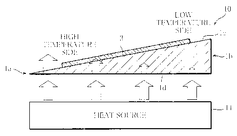
Next, while referring to FIG. 5, a using form of the
thermoelectric conversion module 10 relating to the present
embodiment will be described. Here, FIG. 5 is a sectional
view illustrating a using state of the thermoelectric
conversion module 10 relating to the present embodiment.
[0018] As illustrated in FIG. 5, the thermoelectric
conversion module 10 is arranged so that the second surface
id gets close to a heat source 11. That is, the
thermoelectric conversion module 10 is supplied with heat
trom the side of the second surface ld. Here, for the
insulating film 1 of the thermoelectric conversion module
10, the density is different according to the thickness,
and a thermal conductivity increases as the density
increases. That is, in the insulating film 1, the thermal
conductivity becomes gradually low from the first end la to
the second end lb. Thus, heat of the heat source 11 easily
reaches the thermoelectric conversion element 3 on the side
of the first end la, and the heat of the heat source 11
does not easily reach the thermoelectric conversion element
3 on the side of the second end lb. Thus, in the
thermoelectric conversion element 3, one end positioned on
CA 02936500 2016-07-11
7
the side of the first end 1a of the insulating film 1
becomes a high temperature, the other end positioned on the
side of the second end lb of the insulating film I becomes
a low temperature, and electromotive force by the
temperature difference is generated.
[0019] As described above, since the temperature
difference in the thermoelectric conversion element 3 of
the thermoelectric conversion module 10 relating to the
present embodiment is generated due to a structure of the
insulating film 1, the temperature difference in the
thermoelectric conversion element 3 does not easily vary,
and stable thermoelectric power generation can be performed_
That is, a performance of the thermoelectric conversion
module 10 can be improved, and high reliability can be
achieved.
[0020] In addition, since the thermoelectric conversion
element 3 is formed on the insulating film 1 which is an
Insulator, at a part to be insulated of the thermoelectric
conversion module 10, an excellent insulation
characteristic can be secured. Further, not an end but a
rain surface of the thermoelectric conversion element 3 is
_n contact with the first surface lc of the insulating film
a joined area of the thermoelectric conversion element 3
and the insulating film 1 becomes large, an excellent
joining characteristic of the thermoelectric conversion
element 3 and the insulating film I can be secured, and
joining strength of the thermoelectric conversion module 10
itself can be improved. In other words, in the
thermoelectric conversion module 10, even when dimensions
of the N-type semiconductors and the P-type semiconductors
configuring the thermoelectric conversion element 3 vary, a
joining defect of the thermoelectric conversion element 3
and the insulating film 1 does not occur, and the
CA 02936500 2016-07-11
8
reliability of the thermoelectric conversion module 10 can
be improved.
[0021] Then, since the thermoelectric conversion module
relating to the present embodiment has a relatively
5 simple structure that the thermoelectric conversion element
is formed on the insulating film 1, a manufacturing cost
and manufacturing time can be easily reduced. In
particular, since the thermoelectric conversion module 10
relating to the present embodiment is flexible since it is
10 formed in a film shape, and can be easily installed at
various locations since it is miniaturized.
[0022] As above, for the thermoelectric conversion
module 10 relating to the present embodiment,
miniaturization and improvement of a degree of freedom of
an installation location can be achieved while improving a
performance.
[0023] <Modifications>
In the embodiment described above, a configuration of
installing the heat source 11 on the side of the second
surface ld positioned on the opposite side of a formation
surface of the thermoelectric conversion element 3 is
assumed, however, the heat source 11 may be installed on
the side of the first surface lc. In such a case, a
cooling device may be arranged on the side of the second
surface id and a part where the distance between the first
surface lc and the second surface id is short may be
efficiently cooled compared to the part where it is long so
that the temperature rises from the first end la to the
second end lb.
[0024] In addition, in the embodiment described above,
the flat film member is compressed so that the cross
section of the insulating film 1 becomes a triangle,
however, the shape after the compression is not limited to
CA 02936500 2016-07-11
9
the triangle. For example, as illustrated in FIG. 6 and
FIG. 7, the first surface of the insulating film I may he
curved. More specifically, the first surface lc may be
curved so as to be projected toward an outer side as
Illustrated in FIG. 6, or the first surface lc may be
carved so as to be projected toward an inner side as
illustrated in FIG. 7. In both cases, since the
thermoelectric conversion element 3 is formed into the thin
film shape, it is formed along the shape of the first
surface lc.
[0025] Also, the flat film member may be compressed so
that the insulating film 1 has a gutter-like recess 15 on
the side of the first surface is as illustrated in FIG. 8,
or the flat film member may be compressed so that the
Lnsulating film 1 has a projection 16 on the side of the
first surface lc as illustrated in FIG. 9. In the
thermoelectric conversion module 10 as illustrated in FIG.
8 or FIG. 9, the N-type semiconductors and the P-type
semiconductors need to be connected in series while being
juxtaposed so that, while the part where the distance
hetween the first surface lc and the second surface ld is
the shortest is turned to a high temperature side, the part
here the distance is the longest is turned to a low
temperature side. Note that, while the part where the
distance between the first surface lc and the second
surface id is the longest is turned to the high temperature
side, the part where the distance is the shortest may be
turned to the low temperature side.
[0026] In any case of the modifications illustrated in
FIG. 6 to FIG. 9, effects similar to that of the
thermoelectric conversion module 10 relating to the
embodiment described above can be demonstrated. In
addition, the shape of the insulating film 1 is changed
CA 02936500 2016-07-11
according to a state of an installation location of the
thermoelectric conversion module 10 so that the
thermoelectric conversion module 10 in a shape optimum for
the installation location can be provided.
5 [0027] Further, while the insulating film 1 is disposed
only on one side of the thermoelectric conversion element 3
in the above-described embodiment 1, however, as
illustrated in FIG. 10, the thermoelectric conversion
element 3 may be held by two insulating films 1 and 21.
10 Specifically, as illustrated in FIG. 10, the thermoelectric
conversion element 3 is positioned between the first
surfaces lc and 21c of the two insulating films 1 and 21.
Here, the insulating film 21 has the same structure and
characteristic as the insulating film 1.
[0028] In a thermoelectric conversion module 10 having
such a structure, compared to the thermoelectric conversion
module 10 relating to the embodiment I described above, a
farther excellent insulation characteristic can be secured.
In addition, when the heat source 11 is brought close to
the side of the second surface ld of the insulating film 1
of the thermoelectric conversion module 10', similarly to
the embodiment described above, the first end la becomes
the high temperature side, and the second end lb becomes
the low temperature side. Here, since a second end 21b (an
end where a distance between the first surface 21c and a
second surface 21d is long) of the insulating film 21 is
arranged so as to face the first end la, the heat
transmitted to the thermoelectric conversion element 3 is
not easily transmitted to the second surface 21d.
Therefore, at one end of the thermoelectric conversion
element 3 positioned between the first end la and the
second end 21b, a high temperature state can be excellently
maintained. On the other hand, since a first end 21a (an
CA 02936500 2016-07-11
11
end where the distance between the first surface 21c and a
second surface 21d is short) of the insulating film 21 is
arranged so as to face the second end lb, the heat
transmitted to the thermoelectric conversion element 3 is
easily transmitted to the second surface 21d. Therefore,
.at the other end of the thermoelectric conversion element 3
positioned between the second end lb and the first end 21a,
a low temperature state can be excellently maintained.
That is, in the thermoelectric conversion module 10'
relating to the present modification, since the temperature
difference between both ends of the thermoelectric
conversion element 3 can be easily increased and the
temperature difference can be excellently kept, more
excellent thermoelectric conversion efficiency can be
provided.
[0029] Note that a cooling device such as a heatsink may
be arranged on the second surface 21d, thus the temperature
difference between both ends of the thermoelectric
conversion element 3 can be more increased, the temperature
difference can be excellently kept, and the thermoelectric
conversion efficiency of the thermoelectric conversion
nodule 10' can be further improved.
[0030] <Implementations of the present invention>
The thermoelectric conversion module relating to a
first implementation of the present invention includes a
porous insulating film having an insulation property and a
thermoelectric conversion element in a thin film shape
formed on a first surface of the insulating film, the first
surface includes a surface inclined to a second surface
positioned on an opposite side of the first surface, and a
density of the insulating film increases as a distance
between the first surface and the second surface decreases.
[0031] For the thermoelectric conversion module relating
CA 02936500 2016-07-11
12
to a second implementation of the present invention, in the
thermoelectric conversion module relating to the first
implementation, the insulating film is formed by
compressing a flat film member.
[0032] For the thermoelectric conversion module relating
to a third implementation of the present invention, in the
thermoelectric conversion module relating to the first or
second implementation, the first surface is inclined at a
fixed angle to the second surface.
[0033] For the thermoelectric conversion module relating
to a fourth implementation of the present invention, in the
thermoelectric conversion module relating to the first or
second implementation, the first surface is curved.
[0034] For the thermoelectric conversion module relating
to a fifth implementation of the present invention, in the
thermoelectric conversion module relating to the first or
second implementation, the insulating film includes a
gutter-like recess on a side of the first surface.
[0035] For the thermoelectric conversion module relating
to a sixth implementation of the present invention, in the
thermoelectric conversion module relating to the first or
second implementation, the thermoelectric conversion
element is held by two of the insulating films having the
same shape.
Explanation of Reference Signs
[0036]
1, 21 insulating film
1a, 21a First end
lb, 21b Second end
lc, 21c First surface
ld, 21d Second surface
2 Roller
3 Thermoelectric conversion element
CA 02936500 2016-07-11
13
10, 10 Thermoelectric conversion module
11 Heat source
15 Recess
16 Projection