Note: Descriptions are shown in the official language in which they were submitted.
SPECIFICATION
SYSTEM AND METHOD FOR MANAGING THE POWER OUTPUT OF A
PHOTOVOLTAIC CELL
FIELD
[0001] The present disclosure relates generally to photovoltaic devices and
more specifically, but
not exclusively, to systems and methods for maximizing the power or energy
generated and the
overall efficiency of one or more solar cells, for example, by applying and
adjusting an external
electric field across the solar cells.
BACKGROUND
[0002] A solar cell (also called a photovoltaic cell) is an electrical device
that converts the
energy of light directly into electricity by a process known as "the
photovoltaic effect." When
exposed to light, the solar cell can generate and support an electric current
without being
attached to any external voltage source.
[0003] The most common solar cell consists of a p-n junction 110 fabricated
from
semiconductor materials (e.g., silicon), such as in a solar cell 100 shown in
Fig. 1. For example,
the p-n junction 110 includes a thin wafer consisting of an ultra-thin layer
of n-type silicon on
top of a thicker layer of p-type silicon. Where these two layers are in
contact, an electrical field
(not shown) is created near the top surface of the solar cell 100, and a
diffusion of electrons
occurs from the region of high electron concentration (the n-type side of the
p-n junction 110)
into the region of low electron concentration (the p-type side of the p-n
junction 110).
[0004] The p-n junction 110 is encapsulated between two conductive electrodes
101a, 101b.
The top electrode 101a is either transparent to incident (solar) radiation or
does not entirely cover
the top of the solar cell 100. The electrodes 101a, 101b can serve as ohmic
metal-semiconductor
contacts that are connected to an external load 30 that is coupled in series.
Although shown as
resistive only, the load 30 can also include both resistive and reactive
components.
CA 2937025 2017-06-19
[0005] Typically, multiple solar cells 100 can be coupled (in series and/or
parallel) together to
form a solar panel 10 (shown in Fig. 2). With reference to Fig. 2, a typical
installation
configuration using at least one solar panel 10 is shown. The solar panels 10
can be connected
either in parallel as shown in Fig. 2, series, or a combination thereof, and
attached to a load, such
as an inverter 31. The inverter 31 can include both resistive and reactive
components.
[0006] Returning to Fig. 1, when a photon hits the solar cell 100, the photon
either: passes
straight through the solar cell material¨which generally happens for lower
energy photons;
reflects off the surface of the solar cell; or preferably is absorbed by the
solar cell material¨if
the photon energy is higher than the silicon band gap¨generating an electron-
hole pair.
[0007] If the photon is absorbed, its energy is given to an electron in the
solar cell material.
Usually this electron is in the valence band and is tightly bound in covalent
bonds between
neighboring atoms, and hence unable to move far. The energy given to the
electron by the
photon "excites" the electron into the conduction band, where it is free to
move around within
the solar cell 100. The covalent bond that the electron was previously a part
of now has one
fewer electron¨this is known as a hole. The presence of a missing covalent
bond allows the
bonded electrons of neighboring atoms to move into the hole, leaving another
hole behind. In
this way, a hole also can move effectively through the solar cell 100. Thus,
photons absorbed in
the solar cell 100 create mobile electron-hole pairs.
[00081 The mobile electron¨hole pair diffuses or drifts toward the electrodes
101a, 101b.
Typically, the electron diffuses/drifts towards the negative electrode, and
the hole diffuses/drifts
towards the positive electrode. Diffusion of carriers (e.g., electrons) is due
to random thermal
motion until the carrier is captured by electrical fields. Drifting of
carriers is driven by electric
fields established across an active field of the solar cell 100. In thin film
solar cells, the
dominant mode of charge carrier separation is drifting, driven by the
electrostatic field of the p-n
junction 110 extending throughout the thickness of the thin film solar cell.
However, for thicker
solar cells having virtually no electric field in the active region, the
dominant mode of charge
¨ 2 -
CA 2937025 2017-06-19
carrier separation is diffusion. The diffusion length of minor carriers (i.e.,
the length that photo-
generated carriers can travel before they recombine) must be large in thicker
solar cells.
[0009] Ultimately, electrons that are created on the n-type side of the p-n
junction 110,
"collected" by the p-n junction 110, and swept onto the n-type side can
provide power to the
external load 30 (via the electrode 101a) and return to the p-type side (via
the electrode 101b) of
the solar cell 100. Once returning to the p-type side, the electron can
recombine with a hole that
was either created as an electron-hole pair on the p-type side or swept across
the p-n junction 110
from the n-type side.
[0010] As shown in Fig. 1, the electron-hole pair travels a circuitous route
from the point the
electron-hole pair is created to the point where the electron-hole pair is
collected at the electrodes
101a, 101b. Since the path traveled by the electron-hole pair is long, ample
opportunity exists
for the electron or hole to recombine with another hole or electron, which
recombination results
in a loss of current to any external load 30. Stated in another way, when an
electron-hole pair is
created, one of the carriers may reach the p-n junction 110 (a collected
carrier) and contribute to
the current produced by the solar cell 100. Alternatively, the carrier can
recombine with no net
contribution to cell current. Charge recombination causes a drop in quantum
efficiency (i e , the
percentage of photons that are converted to electric current when the solar
cell 100), and,
therefore, the overall efficiency of the solar cell 100.
100111 The cost of the solar cell 100 or the solar panel 10 is typically given
in units of dollars per
watts of peak electrical power that can be generated under normalized
conditions. High-
efficiency solar cells decrease the cost of solar energy. Many of the costs of
a solar power
system or plant are proportional to the number of solar panels required as
well as the (land) area
required to mount the panels. A higher efficiency solar cell will allow for a
reduction in the
number of solar panels required for a given energy output and the required
area to deploy the
system. This reduction in the number of panels and space used might reduce the
total plant cost,
even if the cells themselves are more costly.
¨ 3 -
CA 2937025 2017-06-19
[0012] The ultimate goal is to make the cost of solar power generation
comparable to, or less
than, conventional electrical power plants that utilize natural gas, coal,
and/or fuel oil to generate
electricity. Unlike most conventional means of generating electric power that
require large
centralized power plants, solar power systems can be deployed at large
centralized locations by
electric utilities, on commercial buildings to help offset the cost of
electric power, and even on a
residence by residence basis.
[0013] Recent attempts to reduce the cost and increase the efficiency of solar
cells include
testing various materials and different fabrication techniques used for the
solar cells. Another
approach attempts to enhance the depletion region formed around the p-n
junction 110 for
enhancing the movement of charge carriers through the solar cell 100. For
example, see U.S.
Patent No. 5,215,599, to Hingorani, etal. ("Hingorani"), filed on May 3, 1991,
and U.S. Patent
8,466,582, to Fornage ("Fornage"), filed on December 2, 2011, claiming
priority to a December
3, 2010 filing date.
[0014] However, these conventional approaches for enhancing the movement of
charge carriers
through the solar cell 100 require a modification of the fundamental structure
of the solar cell
100. Hingorani and Fornage, for example, disclose applying an external
electric field to the solar
cell using a modified solar cell structure. The application of the external
electric field requires a
voltage to be applied between electrodes inducing the electric field
(described in further detail
with reference to equation 2, below). Without modifying the fundamental
structure of the solar
cell 100, applying the voltage to the existing electrodes 101a, 101b of the
solar cell 100 shorts
the applied voltage through the external load 30. Stated in another way,
applying voltage to the
electrodes 101a, 101b of the solar 100 is ineffective for creating an external
electric field and
enhancing the movement of charge carriers. Accordingly, conventional
approaches¨such as
disclosed in Hingoriani and Fornage¨necessarily modify the fundamental
structure of the solar
cell 100, such as by inserting an external (and electrically isolated) set of
electrodes on the base
of the solar cell 100. There are several disadvantages with this approach.
¨ 4 -
CA 2937025 2017-06-19
[0015] For example, the external electrodes must be placed on the solar cell
100 during the
fabrication process¨it is virtually impossible to retrofit the external
electrodes to an existing
solar cell or panel. This modification to the fabrication process
significantly increases the cost of
manufacturing and decreases the manufacturing yield. Additionally, placement
of the external
electrodes over the front, or incident side, of the solar cell 100 reduces the
optical energy which
reaches the solar cell 100, thereby yielding a lower power output.
[0016] As a further disadvantage, to yield significant improvements in power
output of the solar
cell 100, sizeable voltages must be applied to the external electrodes of the
solar cell 100. For
example, Fornage discloses that voltages on the order of "1,000's" of volts
must be placed on the
external electrodes for the applied electric field to be effective and
increase the power output of
the solar cell 100. The magnitude of this voltage requires special training
for servicing as well as
additional high voltage equipment and wiring that does not presently exist in
existing or new
solar panel deployments. As an example, an insulation layer between the
external electrodes and
the solar cell 100 must be sufficient to withstand the high applied voltage.
In the event of a
failure of the insulation layer, there is a significant risk of damage to not
only the solar cell 100,
but also all solar panels 10 connected in series or parallel to the failed
solar cell as well as the
external load 30 (or the inverter 31).
[0017] As a further disadvantage, varying illumination conditions (e.g., due
to cloud coverage of
the sun and/or normal weather fluctuations) can cause instability in the power
output of
conventional solar cells and solar panels. For example, with reference to Fig.
2, the inverter 31
typically requires a static, non-varying voltage and current input. As shown
in Fig. 2, the solar
panels 10 provide the input voltage and current to the inverter 31. However,
time-varying
illumination conditions can cause the output from solar panels 10 to fluctuate
(e.g., on the order
of seconds or less). The fluctuation of the voltage and current supplied to
the inverter 31
compromises the quality of the power output by the inverter 31, for example,
in terms of
frequency, voltage, and harmonic content. Conventional efforts to combat
varying illumination
¨ 5 -
CA 2937025 2017-06-19
conditions include placing batteries or capacitors at the input of the
inverter 31 and,
unfortunately, only minimize these variations.
[0018] In view of the foregoing, a need exists for an improved solar cell
system and method for
increased efficiency and power output, such as with increased mobility of
electron-hole pairs, in
an effort to overcome the aforementioned obstacles and deficiencies of
conventional solar cell
systems.
SUMMARY
[0019] The present disclosure relates to a system for optimizing a power
output of a
photovoltaic device and methods for using and making the same. In accordance
with a first
aspect disclosed herein, there is set forth a method of managing a
photovoltaic device, the
method comprising:
[0020] applying a first component of a voltage signal to a plurality of
photovoltaic devices,
the first component comprising a series of voltage pulses with a positive
magnitude, each of the
voltage pulses representing an on state for generating an external electric
field across the
photovoltaic devices; and
[0021] applying a second component of the voltage signal to the
photovoltaic devices, the
second component representing an off cycle between adjacent voltage pulses.
[0022] In some embodiments of the disclosed method, applying the first
component
comprises applying a high voltage of a time- varying voltage pulse from a
voltage pulser circuit,
and applying the second component comprises shutting off the voltage pulser
circuit.
[0023] In some embodiments of the disclosed method, applying the first
component
comprises connecting a voltage source and the photovoltaic device in a first
position of a switch
disposed between the voltage source and the photovoltaic device, and wherein
said applying the
second component comprises disconnecting the voltage source and the
photovoltaic device in a
second position of the switch.
[0024] In some embodiments of the disclosed method, the method further
comprises
monitoring an output voltage of the photovoltaic device via a voltage probe
coupled across the
¨ 6 -
CA 2937025 2017-06-19
photovoltaic device and monitoring an output current of the photovoltaic
device via a current
sensor coupled in series between the photovoltaic device and a load driven by
the photovoltaic
device.
[0025] In some embodiments of the disclosed method, the method further
comprises
adjusting, via a control circuit coupled to the voltage source, at least one
of a magnitude, a
duration, and a frequency of the first component to maximize a power output
based on said
monitoring.
[0026] In accordance with a another aspect disclosed herein, there is
set forth a method of
managing a photovoltaic device, comprising:
[0027] enabling a voltage source to be coupled to the photovoltaic device;
and
[0028] applying a voltage signal generated by the voltage source to the
photovoltaic device,
the voltage signal having a first state for generating an external electric
field across the
photovoltaic device and a second state representing an off cycle.
[0029] In some embodiments of the disclosed method, enabling the voltage
source comprises
enabling at least one of:
[0030] a voltage pulser circuit to be coupled to the photovoltaic device
for providing a time
varying voltage pulse across the photovoltaic device, the time varying voltage
pulse providing
the first state and the second state; and
[0031] a switch to be coupled between the voltage source and the
photovoltaic device, the
switch connecting the voltage source and the photovoltaic device in a first
position for generating
the first state and disconnecting the voltage source and the photovoltaic
device in a second
position for generating the second state.
[0032] In some embodiments of the disclosed method, applying the voltage
signal comprises
impressing an output of a high voltage source of the voltage pulser circuit
onto the photovoltaic
device when a switching transistor of the voltage pulser circuit is in an on
position for generating
the first state, and continuing said impressing the output of the high voltage
source until a pulse
¨ 7 -
CA 2937025 2017-06-19
generator of the voltage pulser circuit turns the switching transistor to an
off position for
generating the second state.
[0033] In some embodiments of the disclosed method, the method further
comprises
enabling a control circuit to be coupled to at least one of the switch and the
voltage pulser circuit.
[0034] In some embodiments of the disclosed method, the method further
comprises
enabling a voltage probe to be coupled across the photovoltaic device to
monitor an output
voltage of the photovoltaic device and a current sensor to be coupled in
series between the
photovoltaic device and a load of the photovoltaic device to monitor a current
output of the
photovoltaic device.
[0035] In some embodiments of the disclosed method, the method further
comprises
monitoring the output voltage and the output current and adjusting via the
control circuit a
magnitude of the first state to maximize a power output based on said
monitoring.
[0036] In some embodiments of the disclosed method, applying the voltage
signal comprises
generating the external electric field with at least one of a first direction
and a second direction,
the first direction and a polarity of internal electrodes of the photovoltaic
device being in a same
direction for increasing a power output of the photovoltaic device, and the
second direction being
in an opposite direction of the polarity of the internal electrodes for
decreasing the power output.
[0037] In some embodiments of the disclosed method, enabling the voltage
source comprises
enabling the voltage source to be coupled to at least one of a solar cell, an
array of solar cells, a
solar panel, and an array of solar panels.
[0038] In accordance with a another aspect disclosed herein, there is
set forth a method of
managing a photovoltaic device, comprising:
[0039] enabling a voltage pulser to be coupled to a plurality of
photovoltaic devices; and
[0040] applying a voltage signal generated by the voltage pulser to each
of the photovoltaic
devices, the voltage signal having a first state comprising a series of
voltage pulses with a
positive magnitude for generating an external electric field across the
photovoltaic devices and a
second state representing an off cycle between adjacent voltage pulses.
¨ 8 -
CA 2937025 2017-06-19
[0041] In some embodiments of the disclosed method, applying the voltage
signal comprises
applying an adjustable voltage to the photovoltaic device.
[0042] In some embodiments of the disclosed method, the method further
comprises
enabling one or more series inductors to be coupled between the voltage pulser
and a load of the
photovoltaic device for blocking frequencies of the voltage signal to the load
that are greater than
a predetermined frequency.
[0043] In some embodiments of the disclosed method, the method further
comprises
controlling at least one of a frequency and a duration of the first state and
the second state via a
control circuit coupled to the voltage pulser.
[0044] In accordance with a another aspect disclosed herein, there is set
forth a method of
managing a photovoltaic device, comprising:
[0045] enabling a first port of a switch to be coupled to a plurality of
photovoltaic devices;
[0046] enabling a second port of the switch to be coupled to a load
driven by the
photovoltaic devices;
[0047] enabling a third port of the switch to be coupled to a voltage
source, wherein the
switch can operate in a first position for providing a current path between
the photovoltaic
devices and the voltage source and a second position for providing the current
path between the
photovoltaic devices and the load; and
[0048] applying a voltage signal generated by the voltage source to the
photovoltaic devices
when the switch is in a first position, the voltage signal having a first
state comprising a series of
voltage pulses with a positive magnitude for generating an external electric
field across the
photovoltaic devices when the switch is in the first position, and a second
state between adjacent
voltage pulses to provide electrical isolation between the voltage source and
the load when the
switch is in the second position.
[0049] In some embodiments of the disclosed method, enabling the first port
of the switch
comprises enabling a first port of a double throw switch to be coupled to the
photovoltaic device.
¨ 9 -
CA 2937025 2017-06-19
[0050] In some embodiments of the disclosed method, the method further
comprises
controlling at least one of a frequency and a duration of switching between
the first position and
the second position via a switch controller coupled to the double throw
switch.
[0051] In some embodiments of the disclosed method, the method further
comprises
enabling a device for mitigating any voltage drop-out of the first component
to be coupled
between the load and the photovoltaic device.
[0052] In some embodiments of the disclosed method, applying the voltage
signal comprises
applying an adjustable voltage to the photovoltaic device.
[0053] In some embodiments of the disclosed method, the method further
comprises
controlling at least one of a frequency, a magnitude, and a duration of the
first state and the
second state via a control circuit coupled to the voltage source and the
switch based on an output
current of the photovoltaic device measured by a current sensor coupled in
series between the
photovoltaic device and the load and an output voltage of the photovoltaic
device measured by a
voltage probe coupled across the photovoltaic device.
[0054] In accordance with another aspect disclosed herein, there is set
forth a system for
managing a photovoltaic device, comprising:
[0055] a voltage application means being adapted to apply a first
component of a voltage
signal to a plurality of photovoltaic devices, the first component comprising
a series of voltage
pulses with a positive magnitude, each of the voltage pulses comprising an on
state for
generating an external electric field across the photovoltaic devices; and
[0056] the voltage application means being further adapted to apply a
second component of
the voltage signal to the photovoltaic devices, the second component
comprising an off cycle
between adjacent voltage pulses.
[0057] In accordance with another aspect disclosed herein, there is set
forth a system of
managing a photovoltaic device, comprising:
100581 a voltage pulser coupled to a plurality of photovoltaic devices;
and
¨ 10 -
CA 2937025 2017-06-19
[0059] a voltage application means for applying a voltage signal
generated by the voltage
pulser to each of the photovoltaic devices, the voltage signal having a first
state for generating an
external electric field across the photovoltaic devices, the first state
comprising a series of
voltage pulses with a positive magnitude, and a second state comprising an off
cycle between
adjacent voltage pulses.
[0060] In accordance with another aspect disclosed herein, there is set
forth a system for
managing a photovoltaic device, comprising:
10061] a voltage switching means, including: a first port of the voltage
switching means
being enabled to be coupled to a plurality of photovoltaic devices; a second
port of the voltage
switching means being enabled to be coupled to a load driven by the
photovoltaic devices; a third
port of the voltage switching means being enabled to be coupled to a voltage
source, wherein the
voltage switching means is adapted to operate in a first position for
providing a current path
between the photovoltaic devices and the voltage source and a second position
for providing the
current path between the photovoltaic devices and the load;
[0062] and wherein a voltage signal generated by the voltage source is
applied to the
photovoltaic devices, such that the voltage signal has a first state for
generating an external
electric field across the photovoltaic devices when the voltage switching
means is in the first
position, and has a second state to provide electrical isolation between the
voltage source and the
load when the voltage switching means is in the second position.
BRIEF DESCRIPTION OF THE DRAWINGS
[0063] Fig. 1 is an exemplary top-level cross-sectional diagram
illustrating an embodiment
of a solar cell of the prior art.
[0064] Fig. 2 is an exemplary top-level block diagram illustrating one
embodiment of a solar
panel array of the prior art using the solar cells of Fig. 1.
[0065] Fig. 3 is an exemplary top-level block diagram illustrating an
embodiment of a solar
cell management system.
¨ 11 -
CA 2937025 2017-06-19
[0066] Fig. 4 is an exemplary block diagram illustrating an alternative
embodiment of the
solar cell management system of Fig. 3, wherein a solar panel array is coupled
to a voltage
source through a switch.
[0067] Figs. 5A-D are exemplary waveforms illustrating the applied
voltage as a function of
time of the inputs and outputs of the switch used with the solar panel array
of Fig. 4.
[0068] Fig. 6 is an exemplary block diagram illustrating another
alternative embodiment of
the solar cell management system of Fig. 3, wherein a solar panel array is
coupled to a voltage
pulser circuit.
[0069] Fig. 7 is an exemplary waveform illustrating the applied voltage
as a function of time
used with the solar panel array of Fig. 6.
[0070] Fig. 8 is an exemplary block diagram illustrating one embodiment
of the voltage
pulser circuit of Fig. 6.
[0071] Fig. 9A is an exemplary block diagram illustrating an alternative
embodiment of the
solar cell management system of Fig. 4, wherein the solar cell management
system includes a
control circuit.
[0072] Fig. 9B is an exemplary flow-chart illustrating a state diagram
for the control circuit
shown in Fig. 9A.
[0073] Fig. 10A is an exemplary block diagram illustrating an
alternative embodiment of the
solar cell management system of Fig. 6, wherein the solar cell management
system includes a
control circuit.
[0074] Fig. 10B is an exemplary flow-chart illustrating a state diagram
for the control circuit
shown in Fig. 10A.
[0075] Figs. 11A-C are exemplary waveforms illustrating an embodiment of
the relationship
between applied voltage, pulse frequency, and pulse width to the improved
current output of the
photovoltaic device of Fig. 3.
[0076] It should be noted that the figures are not drawn to scale and
that elements of similar
structures or functions are generally represented by like reference numerals
for illustrative
¨ 12 -
CA 2937025 2017-06-19
purposes throughout the figures. It also should be noted that the figures are
only intended to
facilitate the description of the preferred embodiments. The figures do not
illustrate every aspect
of the described embodiments and do not limit the scope of the present
disclosure.
DETAILED DESCRIPTION OF THE PREFERRED EMBODIMENTS
[0077] Since currently-available solar cell systems fail to maximize the
power output of a
photovoltaic cell, a solar cell system that increases the mobility of electron-
hole pairs and
reduces the recombination current in a semiconductor material can prove
desirable and provide a
basis for a wide range of solar cell systems, such as to increase the
efficiency and power output
of solar cells configured as a solar panel. This result can be achieved,
according to one
embodiment disclosed herein, by a solar cell management system 300 as
illustrated in Fig. 3.
[0078] Turning to Figure 3, the solar cell management system 300 is
suitable for use with a
wide range of photovoltaic devices. In one embodiment, the solar cell
management system 300
can be suitable for use with the solar cell 100 shown in Fig. 1. For example,
the solar cell 100
can represent any suitable generation of solar cells such as wafer-based cells
of crystalline silicon
(first generation), thin film solar cells including amorphous silicon cells
(second generation),
and/or third generation cells. The solar cell management system 300
advantageously can be used
with any generation of solar cell 100 without structural modification¨and the
associated
drawbacks.
[00791 In another embodiment, the solar cell management system 300 can
be suitable for use
with multiple solar cells 100, such as the solar panels 10 shown in Fig. 2. As
previously
discussed, multiple solar cells 100 can be coupled (in series and/or parallel)
together to form a
solar panel 10. The solar panels 10 can be mounted on a supporting structure
(not shown) via
ground mounting, roof mounting, solar tracking systems, fixed racks, and so on
and can be
utilized for both terrestrial and space borne applications. Similarly, the
solar cell management
system 300 advantageously can be used with any generation of solar panel 10
without structural
modification¨and the associated drawbacks¨of the solar panel 10.
¨ 13 -
CA 2937025 2017-06-19
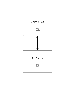
[0080] As shown in Fig. 3, the photovoltaic device 200 cooperates with
an electric field 250.
In some embodiments, the polarity of the electric field 250 can be applied in
either the same
direction or the reverse direction as the polarity of the electrodes 101a,
101b (shown in Fig. 1) in
the photovoltaic device 200. For example, if applying the electric field 250
in the same direction
as the polarity of the electrodes 101a, 101b in the photovoltaic device 200,
the electric field 250
acts on the electron-hole pairs in the photovoltaic device 200 to impose a
force¨CE or h*E on
the electron or hole, respectively¨thereby accelerating the mobility of the
electron and hole
towards respective electrodes. Alternatively, if the polarity of the electric
field 250 is reversed,
the mobility of the electron-hole pairs in the photovoltaic device 200
decreases, thereby
increasing the recombination current within the photovoltaic device 200.
Accordingly, the
efficiency of the photovoltaic device 200 can be diminished as desired, such
as for managing the
power output of the photovoltaic device 200.
[0081] Furthermore, the electric field 250 applied to the photovoltaic
device 200 can be static
or time varying as desired. In the case where the electric field 250 is time
varying, the electric
field 250 has a time averaged magnitude that is non-zero. Stated in another
way, the net force on
the electrons and holes is non-zero to provide increased mobility in the
electron-hole pairs of the
photovoltaic device 200.
[0082] If applied to the conventional solar cell 100 of Fig. 1, in the
absence of an external
load 30 (shown in Fig. 1), an external voltage can be applied across the
electrodes 101a, 101b of
the solar cell 100 to create the electric field 250. In one embodiment, the
electric field 250 (e.g.,
between the electrodes 101a, 101b) is defined by Equation 1:
E = (VApp ¨ Vp)
(Equation 1)
[0083] In Equation 1, E represents the electric field 250, VA pp is the
voltage applied
externally to the photovoltaic device 200, Vp is the voltage output of the
photovoltaic device 200
(e.g, ¨ 30 volts), and t is the thickness of the semiconductor material in the
photovoltaic device
200 from electrode 101a to 101b. For example, assuming VA pp ¨ Vp = 200 Volts
(nominally)
¨ 14 -
CA 2937025 2017-06-19
and a thickness t of about 0.02 cm, the electric field 250 is about 10K
Volts/cm. It can be seen
from Equation 1 that as the thickness t of the photovoltaic device 200
decreases (e.g., less than
0.01 cm), higher electric fields 250 can be generated using the same or lower
voltages.
[0084] As discussed above, the photovoltaic device 200 typically drives
an external load,
such as the load 30 of the solar cell 100. With reference to Equation 1, if
applying an external
voltage VApp directly to the photovoltaic device 200 that drives the external
load 30, the external
load 30 can include resistive components that draw current from the source of
the applied
voltage 174fifi. Stated in another way, applying the external voltage VApp to
the photovoltaic device
200 can effectively deliver power to the overall circuit represented by
Equation 2:
(VA)
2
PUWerinput
RL (Equation 2)
100851 In Equation 2, RL represents the impedance of the external load
30. In some cases,
the input power can be substantially greater than the power output of the
photovoltaic device
200. Accordingly, the solar cell management system 300 is configured to apply
the electric field
250 across the photovoltaic device 200 without injecting more energy than the
photovoltaic
device 200 is capable of producing or more energy than would be gained by
applying the electric
field across the photovoltaic device 200.
[0086] The solar cell management system 300 can apply the external
voltage VApp to the
photovoltaic device 200 using any suitable means described herein, including
using a switch 55
as shown in Fig. 4. Turning to Fig. 4, the photovoltaic device 200 can
represent any number of
photovoltaic devices such as the solar cell 100 and/or the solar panels 10 as
illustrated. The solar
panels 10 are connected to the switch 55, such as a single pole, double throw
(or three-way)
switch as shown. In one embodiment, the switch 55 is also coupled to a voltage
source 50 and
an external load RL (e.g., shown as the inverter 31). The inverter 31 can
convert a DC voltage
and current into an AC voltage and current, which is typically compatible in
voltage and
frequency with conventional AC power grids. The output frequency of the
inverter 31 and the
¨ 15 -
CA 2937025 2017-06-19
amplitude of the AC current/voltage can be based upon country, location, and
local grid
requirements.
[0087] The voltage source 50 can include any suitable means for
maintaining a constant
voltage, including ideal voltage sources, controlled voltage sources, and so
on. However, in
_______________________________________________________________ some
embodiments¨such as the embodiment shown below with reference to Fig. 9A
the
voltage source 50 can have a variable, adjustable output (e.g., time varying
voltage). A switch
control (or controller) 45 is coupled to the switch 55 to control the duration
of connection and/or
the frequency of switching, such as between the voltage source 50 and the
inverter 31 to the solar
panels 10. The switch controller 45 can be preset to operate at a fixed
switching duration D and
switching frequency f(shown in Figs. 5A-C). The voltage applied in the first
position of the
switch 55 can be fixed and based on the voltage source 50. In some
embodiments, the
magnitude of the voltage applied by voltage source 50, the duration D of
connection, and/or the
frequency f of switching can be preset and/or vary based on load conditions.
[0088] For example, the switch 55 connects the solar panels 10 with the
voltage source 50 in
a first position (as shown with the arrow in the switch 55 of Fig. 4). When
connected in the first
position, the voltage source 50 applies a voltage VAPP across the electrodes
101a, 101b (shown in
Fig. 1) of the solar panels 10 and induces the electric field 250 (shown in
Fig. 3) across each
solar panel 10. Once the electric field 250 has been established across the
solar panels 10, the
switch 55 switches to connect the solar panels 10 to the inverter 31 (i.e.,
the load RL) in a second
position. Accordingly, the voltage source 50 can provide the electric field
250 without being
connected to the solar panels 10 and the inverter 31 at the same time.
Therefore, with reference
again to Equation 2, applying the external voltage VApp does not allow the
load RL (e.g., the
inverter 31) to draw current directly from the voltage source 50.
[0089] Application of the electric field 250 to the solar panels 10 can
increase the current and
power output of the solar panels 10 by a predetermined amount when the solar
panels 10
subsequently are connected to the inverter 31 in the second position. The
predetermined amount
is dependent upon an intensity of light incident on the solar panels 10, the
voltage applied VApp to
¨ 16 -
CA 2937025 2017-06-19
the solar panels 10 by the voltage source 50, the thickness of the solar
panels 10, the frequency f
that the voltage source 50 is connected to the solar panels 10, and the duty
cycle of the switching
process between the first position and the second position¨with the duty cycle
being defined as
the amount of time that the solar panels 10 are connected to the voltage
source 50 divided by 1/f
the switching time (i.e., multiplied by the frequency f or divided by the
total period of the signal).
It should be noted that the switch duration time D, the switching frequency f,
and the duty cycle
are all interrelated quantities such that quantifying any two of the
quantities allows for
determination of the third quantity. For example, specifying the switching
frequency and the
duty cycle allows for determination of the switch duration time D. For
example, under high
intensity light conditions, the improvement in power output can be on the
order of 20%; under
low light conditions, 50+%.
[0090] The embodiment shown in Fig. 4 advantageously provides the
electric field 250 to the
photovoltaic device 200 without the need to modify the solar panels 10 and/or
solar cells 100 to
include additional, external electrodes.
[0091] _______________________________________________________ In some
embodiments, an energy storage device such as a capacitor 41, an inductor
42, and/or a battery 43¨can be placed before the inverter 31 to mitigate any
voltage drop-out
being seen by the inverter 31 while the switch 55 is in the first position.
Accordingly, while the
inverter 31 (i.e., load) is disconnected from the solar panels 10 when the
switch 55 is in the first
position and the electric field 250 is being established across the solar
panels 10 (i.e., switching
time D shown in Figs. 5A-D), the energy storage device supplies energy to the
inverter 31 to
keep current flowing during this switched period. Stated in another way, the
energy storage
device can discharge while the solar panels 10 are disconnected from the
inverter 31.
[0092] Therefore, a constant voltage from the voltage source 50¨which in
turn creates the
electric field 250 ________________________________________________________
need not be applied continuously to see an improvement in the power output
of the solar panels 10. For example, with duration switching times D of
nominally 10-2000ns,
VArp's of nominally 100-500+ Volts, and a switching frequency f of 20
seconds, the duty cycle
of nominally 0.1-10% can be used. The inductor 42, the capacitor 41, and/or
the battery 43 are
¨ 17 -
CA 2937025 2017-06-19
chosen to be of sufficient size to provide enough discharge while the solar
panels 10 are
disconnected while the electric field 250 is being placed across the solar
panels 10 so as not to
cause a drop out on the output of the inverter 31.
[0093] For example, the size of the capacitor 41 that is placed across
the load (e.g., the
inverter 31) is determined by the acceptable voltage droop that the inverter
31 can tolerate during
the switching time D. For example, if the voltage droop during the switching
time D is not to be
less than 90% maximum voltage generated by the photovoltaic device 200, the
capacitor needs to
be sized such according to Equation 3:
¨D
C41 = ___________________________________
&in (May V) (Equation 3)
[0094] In Equation 3, D is the duration the switch is connected to the
voltage source 50 and
MaxV is the percentage of the maximum voltage required (e.g., 90% in the
example above). In a
similar manner, the inductance and/or the battery can be calculated.
[0095] Fig. 5A illustrates control voltage as a function of time from
the switch controller 45
to activate and control the switch 55 using the solar cell management system
300 of Fig. 4. In
this example, the solar panels 10 are disconnected from the inverter 31 and
connected to the
voltage source 50 in the first position of the switch 55 for the duration D,
which is repeated every
1/f seconds. Fig. 5B illustrates the voltage as a function of time from the
voltage source 50
provided to the switch 55 at the first position. Fig. 5C illustrates the
output voltage of the switch
55 from the solar panels 10 (when wired in parallel) as a function of time at
the output of the
switch 55 that couples to the inverter 31 in the second position. Similarly,
Fig. 5D illustrates the
voltage as a function of time at the output of the switch 55 that couples to
the inverter 31 having
a capacitor 41 coupled there between.
[0096] The drop in voltage seen by the inverter 31 shown in Fig. 5D at
the end of the
switching duration D is designated the voltage droop discussed above. The
voltage droop is
dependent on the size of the capacitor 41, the inductor 42, and/or the battery
43. In one example
of the system 300 that does not include the capacitor 41, the inductor 42, or
the battery 43, the
¨ 18 -
CA 2937025 2017-06-19
voltage applied across the input of the inverter 31 appears as the output
voltage illustrated in Fig.
Sc.
[0097] Fig. 6 illustrates an alternative embodiment of the solar cell
management system 300
of Fig. 3. Turning to Fig. 6, the photovoltaic device 200 can represent any
number of
photovoltaic devices such as the solar cell 100 and/or the solar panels 10 as
illustrated. As
shown, the solar panels 10 are wired in parallel, but can also be wired in
series and any
combination thereof.
[0098] A voltage pulser 60, such as a high voltage pulse generator, can
apply a time varying
voltage pulse 71 (shown in Fig. 7) across one or more of the solar panels 10.
In one
embodiment, a duration Dp of the voltage pulse 71 can be short¨nominally 10-
2000 ns¨and a
magnitude can be high¨nominally 100-500+ Volts. In the embodiment shown in
Figure 6, the
voltages applied, the pulse width, and the pulse repetition rate are fixed at
a predetermined level
to provide optimum performance under selected operating conditions. For
example, with
reference to Figs. 6 and 7, the voltage pulse 71 has the duration Dp of about
1000 ns, which
voltage pulse 71 is repeated with a period of 1/f. The duration Dp of the
voltage pulse 71 and the
frequencyfof the voltage pulse 71 are chosen such that the reactance of
inductors in the voltage
inverter 31 present a high impedance to the voltage pulser 60, which high
impedance allows a
high voltage to be developed across the electrodes 101a, 101b (shown in Fig.
1) of the solar
panels 10 and not be shorted out by the inverter 31.
[0099] Additionally, series inductors (not shown) can be placed at the
input of the inverter
31, which series inductors are capable of handling the current input to the
inverter 31 and act as
an RF choke such that the voltage pulses 71 are not attenuated (or effectively
shorted) by the
resistive component of the inverter 31. The duty cycle (time the pulse is
on/time the pulse is oft)
can be nominally 0.1-10%.
[0100] The strength of the electric field 250 imposed on the photovoltaic
device 200 is a
function of the construction of the photovoltaic device 200, such as the
thickness of the
¨ 19 -
CA 2937025 2017-06-19
photovoltaic device 200, the material and dielectric constant of the
photovoltaic device 200, the
maximum breakdown voltage of the photovoltaic device 200, and so on.
[0101] For the voltage pulse 71 shown in Fig. 7, a Fourier analysis of
this waveform results
in a series of pulses with frequencies co = ncoo where coo = 2nf and the
strength of the pulses is
given by Equation 4:
cc
sin rutT
V(cd)= 21rr VApp
nn-r
71= ¨CO (Equation 4)
[0102] In Equation 4, n is a series of integers from -.0 to +00.
Accordingly, the 0th order
pulse (i.e., n=0) has a DC component that is shorted through the resistive
load RL. The first
order of the voltage pulse 71 applied across the solar panels 10 is VApp (1 ¨
Dp 11), where Dp/fis
the duty cycle of the pulse, Dp is the pulse duration, and fis the repetition
rate of the pulse.
Since the inductance of the inverter 31 acts as a high impedance Z to the
voltage pulse 71
generated by the embodiment of Fig. 6, a high voltage pulse 71 is developed
across each of the
solar panels 10, which, in turn, creates a high electric field 250 across the
solar panels 10.
[0103] As shown in Fig. 6, the voltage inverter 31 represents the external
load RL. However, the
external load RL can include purely resistive components such that a set of
inductors can be
placed in series with the load RL to act as the RF choke so that the voltage
pulse 71 (and the
electric field 250) is applied across the solar panels 10.
[0104] Any number of circuits can be used in the voltage pulser 60 to apply
the voltage pulse 71
as desired. One such exemplary circuit used in the voltage pulser 60 is shown
in Fig. 8. As
illustrated, the voltage pulser 60 includes a pulse generator 61 (not shown),
a high voltage source
69 (not shown), and a switching transistor 68 for impressing the high voltage
pulse 71 on the
solar panels 10 (e.g, by switching the output of the high voltage source 69 to
the solar panels 10)
shown in Fig. 6. The voltage pulser 60 of Fig. 8 contains a device that
transfers electrical signals
between two, electrically isolated, circuits using light, such as an opto-
isolator 62 to isolate the
pulse generator 61 from the high voltage switching transistor 68.
Advantageously, the opto-
- 20 ¨
CA 2937025 2017-06-19
isolator 62 prevents a high voltage (e.g., from the high voltage source 69)
from affecting the
pulse signal 71. The opto-isolator circuit 62 is illustrated with pins 1-8 and
is shown as part of
the input circuit to the voltage pulser 60.
[0105] A bias voltage supply 63 (not shown) provides voltage (e.g., 15 VDC) to
the opto-isolator
62 to supply the required bias for the opto-isolator 62. A capacitor 64
isolates the bias voltage
supply 63, creating an AC path for any signal from distorting the bias supply
to the opto-isolator
62. Pins 6 and 7 of the opto-isolator 62 are the switching signal output of
the opto-isolator 62
used to drive the high voltage switching transistor 68. A diode 66¨such as a
Zener diode¨is
used to hold the switching threshold of the switching transistor 68 to above
the set point of the
diode 66, eliminating any noise from inadvertently triggering the switching
transistor 68.
Resistor 67 sets the bias point for the gate G and emitter E of the switching
transistor 68. When
the voltage applied across pins 6 and 7 of the opto-isolator 62 exceeds the
threshold set by the
resistor 67, the switching transistor 68 is turned "on" and current flows
between the collector C
and the emitter E of the high voltage switching transistor 68. Accordingly,
the high voltage
switching transistor 68 presents an Injected High Voltage source to the solar
panels 10 until the
Control Pulse IN from the pulse generator 61 drops below the set threshold on
the G of the high
voltage switching transistor 68, which stops the current flow across C-G
shutting the switching
transistor 68 "off"
101061 As in the previous embodiments described above, application of
the electric field 250
to the solar panels 10 can increase the current and power output of the solar
panels 10 when
subsequently connected to the inverter 31 by a predetermined amount (e.g.,
dependent upon the
intensity of light incident on solar panels 10, the voltage applied VApp to
the solar panels 10 by
the voltage source 50, the thickness of the solar panels 10, the pulse width
Dp, and the frequency
fthat the voltage pulse 71 is applied to the solar panels 10, and so on).
Similarly, under high
intensity light conditions, the improvement in power output of the solar
panels 10 can be on the
order of 20%; and under low light conditions can be 50+%.
¨ 21 -
CA 2937025 2017-06-19
[0107] The improvement in the performance of the photovoltaic device 200
cooperating with
the electric field 250 can be measured as an increase in the short circuit
current of the solar cell,
as shown in Equation 5:
'Sc¨ 1-Base [1 C.(V (I, f E)*(Pmax¨ (Equation 5)
[0108] where /Base is the short circuit current when no external electric
field 250 is applied
and pmax is the maximum optical power whereby any additional power does not
create any
additional electron-hole pairs. As the improvement in the current output of
the solar cell is
driven by the electric field 250, the form of c(Ver, 0,t,c) can be described
by Equation 6:
c(V(r, f), t, c) = m(t, c)VApp*(1-exp(rtro ))*exp(-hecay/f)
(Equation 6)
[0109] In Equation 6, m(t, c) is dependent on the photovoltaic device 200.
The improvement
in the short circuit current Lc due to the electric field 250 can be linear
with respect to the applied
voltage VApp. The improvement observed with respect to the pulse repetition
rate has a
characteristic decay rate of (1 õfiecay) and to behave exponentially with
respect to the pulse ratef
The improvement observed with respect to the pulse width T can also behave
exponentially and
describe how quickly the applied voltage VApp, reaches full magnitude. The
improvement
observed with respect to the pulse width T is dependent upon the details of
the voltage pulser 60.
The increase in the short circuit current Iõ, as a function of applied voltage
VAõ, the pulse
repetition rate f, and the pulse width T, are shown in Figs. 11A-C,
respectively.
[0110] Fig. 11A shows the expected improvement in the short circuit
current Ise, for the solar
panel 10 (shown in Fig. 2) as a function of the magnitude of the applied
voltage pulse V App. As
shown, the pulse width and the pulse repetition rate are fixed and the
magnitude of the pulse
voltage is varied from 50 to 250 volts. The improvement in the short circuit
current AIsc
increases from nominally 0.1 to 2 Amps. The change in the short circuit
current AIsc as a
function of the applied voltage pulse V App is, to first order, approximately
linear. Fig. 11B shows
the change in the improvement of the short circuit current AIsc as a function
of the pulse
¨ 22 -
CA 2937025 2017-06-19
repetition rate for a fixed pulse width and a fixed voltage pulse. As shown in
Fig. 11B, the
improvement in the short circuit current AIsc decreases from approximately 1.7
amps to about
0.45 amps as the pulse repetition rate increases from 10 to 100 in arbitrary
time units. This
behavior is approximately exponential. Fig. 11C shows the change in the
improvement of the
short circuit current AIsc as a function of the pulse width for a fixed pulse
repetition rate and a
fixed voltage pulse. For this example, the improvement of the short circuit
current, AIsc
increases from 0 to 1.2 amperes as the pulse width increases from 0 to 2000
over time.
[0111] In each of the described embodiments, increasing the strength of
the electric field 250
across the electrodes 101a, 101b of the solar cell 100 or solar panel 10
increases the efficiency of
the solar cell 100 or panel 10, for example, up to a maximum electric field
strength of Emax=
Stated another way, once the strength of the electric field 250 reaches a
maximum strength, the
electron-hole recombination rate has been minimized. Accordingly, it can be
advantageous to
configure the control circuit of the photovoltaic device 200 to maximize the
output current and
voltage under varying operating conditions.
[0112] For example, turning to Fig. 9A, a current sensor 33 and a voltage
probe 32 are
shown coupled to the solar cell management system 300 of Fig. 4. As
illustrated, the current
sensor 33 is coupled in series between the solar panel 10 and the inverter 31.
The current sensor
33 can monitor the current output of the solar panel 10. Similarly, the
voltage probe 32 is
connected across the solar panels 10 and the inverter 31 to monitor the output
voltage of the solar
panel 10.
[0113] A control circuit 35 is coupled to both of the current sensor 33
via control leads 33a
and the voltage probe 32 via control leads 32a. The current sensor 33 can be
an inline or
inductive measuring unit and measures the current output of the solar panels
10. Similarly, the
voltage sensor 32 is used to measure the voltage output of the solar panels
10. The product of
the current measured from the current sensor 33 and the voltage measured from
the voltage
probe 32 is the power output from the solar panels 10 to the inverter 31.
¨ 23 -
CA 2937025 2017-06-19
[0114] In some embodiments, the voltage probe 32 may also serve as a
power source for the
control circuit 35 and is active only as long as the solar panels 10 are
illuminated and provide
sufficient power to activate control circuit 35. The control circuit 35
further is coupled to the
switch 55 to determine switching times and frequency discussed with reference
to Fig. 4. The
duration of the switching times and the frequency can be controlled to apply
the voltage VAN,
across the solar panels 10 such that both the current generated within the
solar cell 100 and
measured by the current sensor 33 and voltage probe 32 are maximized under
various operating
conditions, such as under differing or variable lighting conditions.
[0115] In one embodiment for applying the electric field 250, the solar
panel 10 initially does
not generate power, for example, during the night or heavy cloud coverage. As
the solar panels
10 are illuminated (for example, during the morning), voltage and current are
generated by the
solar panels 10, and the leads 32a begin to deliver both current and voltage
to the control circuit
35. The control circuit 35 contains a low voltage logic power supply (not
shown) to drive
control logic within the control circuit 35. The control circuit 35 also
includes the power source
50 for providing a high voltage power supply. The voltage source 50 has a
variable output which
can be adjusted by the control circuit 35 and is responsible for placing VApp
on a lead 38. The
high voltage output VApp from the control circuit 35 drives the lead 38 and is
connected to the
switch 55. The lead 38 is used to apply voltage VA pp through the switch 55 to
the solar panels 10.
In this example, the control circuit 35 is configured not to apply any voltage
VAN, to the solar
panels 10 until enough power is generated by the solar panels 10 to activate
both the low voltage
logic power supply and the high voltage power supply.
[0116] In an alternative embodiment, the control circuit 35 can be
configured to apply the
electric field 250 and maximize the power output as the illumination in the
day increases and
decreases. The control circuit 35 can provide the electric field 250 and
stabilize the power
output of the solar panels 10 according to any method described above,
including process 9000
shown in Fig. 9B.
¨ 24 -
CA 2937025 2017-06-19
[0117] Turning to Fig. 9B, the process 9000 includes initializing power,
at step 900. Enough
power must be present from the output of the solar panels 10 to activate both
the low voltage
logic power supply, which operates the control logic in control circuit 35,
and the high voltage
power supply necessary to place a high voltage on the lead 38 and through the
switch 55.
Alternatively, the control circuit 35 can be powered from an external source
(not shown)¨for
example, a battery, a large capacitor, an external AC power supply¨which
allows the low voltage
logic power supply to operate and the control circuit 35 to monitor the power
output of the solar
panels 10 until the solar panels 10 generate enough power output to warrant
applying the electric
field 250 on the solar panels 10 to augment their power output. Since the
control circuit 35 is
starting up, all of the parameters (e.g., the applied high voltage VApp, the
switch duration time D,
and the switching frequency!) are initialized. In one embodiment, the applied
high voltage Viipp
is set to zero while the switching duration D and the switching frequency f
are set to nominal
values of D=r, andf=f0. All of the control indices, n, 1, and j are
initialized to zero.
[0118] The control circuit 35 then determines, at step 901, whether the
voltage as measured
on the voltage probe 32 is above or below a predetermined minimum võ,;,, and
whether the
current as measured on the current sensor 33 is above a predetermined minimum,
im,õ. The
combination of vm,, and imin have been chosen such that the solar panels 10
are determined to be
illuminated and generating some nominal percentage, for example, 5%, of their
average rated
power and that there is enough power being generated to supply the power
source 50 within the
control circuit 35 to augment the output of the solar panels 10. If the
control circuit 35
determines that both the measured current and voltage are above the respective
predetermined
minimums, the control circuit 35 is now operational and process 9000 moves to
step 903;
otherwise, the process 9000 goes into a wait state, at step 902, and returns
to step 900.
[0119] In step 903, the control circuit 35 measures the current flowing
into the inverter 31
via the current sensor 33, the voltage across the inverter 31 via the voltage
sensor 32, and
calculates the power (nominally, current x voltage) flowing through the
inverter 31. A control
index n is incremented to n +1.
¨ 25 -
CA 2937025 2017-06-19
101201 In step 904, the control circuit 35 compares VA pp with Vmax.
Vmax can be a preset
value and represents the maximum voltage that can be placed on the solar
panels 10 without
damaging either the solar panels 10 or the inverter 31. Depending upon the
type of the solar
panel 10, \Tina, is typically between 600 V and 1,000 V. If VA pp is less than
Vmax, then process
9000 proceeds to step 906; otherwise, process 9000 waits in step 905.
101211 In step 906, the control circuit 35 increments the applied high
voltage VA,,,, by an
amount nAV, and activates the switch 55. Activating the switch 55 disconnects
the solar panels
from the inverter 31 and connects the solar panels 10 to VA,,,, from the
control circuit 35 on
leads 38. For this example, AV can be a fixed voltage step of 25 Volts
although larger or smaller
10 voltage steps can be used. The voltage VA,,,, imposes the electric field
250 on the solar panels 10
such that the strength of the electric field 250 is proportional to the
applied voltage VA,,,,. The
duration of the connection of the solar panels 10 to VA,,,, within the control
circuit 35 is chosen to
not interrupt operation of the inverter 31. For this example, the duty cycle
is chosen to be 5%
(the solar panels 10 are connected 5% of the time to VApp within the control
circuit 35) and the
default duration of the switching time is chosen to be nominally 1000ns.
Alternative switching
times can be used as desired. The control circuit 35 again receives the
measurement of the
current flowing into the inverter 31 via the current sensor 33, receives the
measurement of the
voltage across the inverter 31 via the voltage sensor 32, and recalculates the
power flowing
through the inverter 31.
[0122] In step 908, the control circuit 35 compares the power output of the
solar panels 10
before VApp was placed on the solar panel 10 to the most recent measurement.
If the power has
increased, the process 9000 returns to step 901 and is repeated. The voltage
applied on the lead
38 is increased by AV until either the applied high voltage VA,, p is greater
than Viudx or until the
increase in the applied high voltage VA,,,, does not yield an increase in
output power of the solar
panels 10. Võ,aõ is defined here as the maximum voltage that can be placed on
a solar panel
without causing it any damage. Depending upon the type of the solar panel 10,
V,,õõ is typically
¨ 26 -
CA 2937025 2017-06-19
approximately 600 to 1,000 V. In both cases, process 9000 waits in step 905.
The duration of
the wait state could be from seconds to minutes.
[0123] After the wait step 905, process 9000 continues to step 907. If
the power, as
measured through the leads 32a and 33a, has not changed, the index n is
decremented (n=n-1),
the applied voltage VA pp on the leads 38 to the solar panel(s) 10 is
decreased by the amount AV,
and the control circuit 35 activates the switch 55. Process 9000 continues in
step 909 where the
power output is measured by the current sensor 33 and voltage probe 32. If the
power output
shows a drop, process 9000 continues to step 910. If the power output has
increased, the process
9000 returns to step 907 and the applied voltage VApp continues to decrement
until the power
output of the solar panels 10 ceases to diminish. The process 9000 proceeds to
step 910.
[0124] In step 910, the control circuit 35 increases the duration that
the switch 55 is
connected to the solar panels 10 on the lead 38 in the first position
discussed above. The amount
of time that the switch 55 is connected to the voltage source 50 is increased
by an amount aro.
The switch 55 is activated and the power output of the solar panels 10 is
again monitored by the
current sensor 33 and the voltage probe 34. The process 9000 proceeds to state
912 to determine
whether the power output of the solar panels 10 increases. If so, process 9000
moves to step 910
and the duration that the solar panels 10 are connected to the voltage source
50 is increased
again. The switching duration will increase until the output power of the
solar panels 10 reaches
a maximum (or until a fixed duration limit ¨ for example, 3-5 seconds is
reached) ¨ at which
point the switch duration changes driven by the control circuit 35 stops.
However, if at step 912,
the control circuit 35 determines that increasing the switch duration D causes
a decrease in the
power output as measured by the current sensor 33 and the voltage probe 32,
process 9000
continues to step 911 and the switch duration D is decreased by iterating
between steps 911 and
913 until the power output of the solar panels 10 is maximized again. After
the control circuit 35
has determined that the switching duration has been optimized for maximum
output power of
solar panels 10 by repeating step 910 to step 913, process 9000 continues to
step 914.
¨ 27 -
CA 2937025 2017-06-19
[0125] In step 914, the control circuit 35 begins to increase the
frequency of connection f at
which the switch 55 is connected to the control circuit 35. The frequency f
that the switch 55 is
connected to the voltage source 50 is increased by j4f from the original
switching frequency f0
such that f = +j4f In step 914, the switch 55 is connected between the lead 38
and the solar
panels 10 at a new frequency, f, and the power output of the solar panels 10
is again monitored
by the current sensor 33 and the voltage probe 34. The process 9000 continues
to step 916. If
the power output of the solar panels 10 has increased, the process 9000 moves
back to step 914
and the rate at which the solar panels 10 are connected to the voltage source
50 is increased
again. The rate of connection will increase until the output power of the
solar panels 10 reaches
a maximum or until a maximum frequency fmõ, at which point the process 9000
moves to step
915. In step 914, the frequency the switch 55 connects to the high voltage 50
on the lead 38 is
now decremented by an amount j/If and the switch 55 is activated again and the
power output of
the solar panels 10 is again monitored by the current sensor 33 and the
voltage probe 32. At that
point, the control circuit 35 decides whether the decrease in the rate of
connection increases the
power output of solar panels 10 in step 917. If so, the process 9000 returns
to step 915.
Alternatively, if the frequency of switching reaches some minimum
frequencyfmm, the process
9000 moves to step 918 to wait.
[0126] In step 918, once the power output of the solar panels 10 has
been maximized, the
control circuit 35 goes into a wait state for a period of time. The period of
wait time can be
seconds or minutes. After waiting in step 918, the process 9000 moves to step
901 where
process 9000 again begins to vary the voltage, the switch connection time and
the switching rate
from the previous optimized values to validate the solar panels 10 are still
operating at their
maximum output levels. The applied voltage 50 from the control circuit 35, the
switching
duration, and the switching rate are all varied over the course of operation
during a day to be sure
that the solar panels 10 arc operating under with maximum output power under
the operational
conditions of that particular day.
¨ 28 -
CA 2937025 2017-06-19
[0127] If at step 901, the voltage as measured on voltage sensor 32
drops below the
predetermined minimum vmm, and the current as measured on current sensor 33
drops below a
predetermined minimum imm, the control circuit 35 will remove any voltage on
lines 38, and the
control circuit 35 will move to step 902 to wait before returning to step 900
(where the system
will reinitialize all of the parameters and indices). Process 9000 will
alternate from step 900 to
901 to 902 to 900 until both the voltage as measured on the voltage probe 32
and the current as
measured on the current sensor 33 are both above vnnn and inn respectively, at
which point the
process 9000 will move from step 901 to step 903.
[0128] Different state machines within control circuit 35 can be
implemented to yield similar
results and are covered by this disclosure. However, the process 9000
described above
advantageously minimizes the magnitude of the applied voltage VA pp to the
lowest value possible
such that the product of the current measured by the current probe 33 and the
voltage measured
by the voltage probe 32 are maximized. The applied voltage VA pp is dithered ¨
that is changed by
small amounts both up and down - over the course of operation in a day to
account for changes
the incident optical power, p, on the solar cell 100, the solar panel 10, or
the plurality of solar
panels 10 over the course of a day so that the maximum power output can always
be maintained.
[0129] Most of the steps described in process 9000 above were designed
to address adiabatic
changes in illumination that occur slowly over periods of multiple minutes or
hours. In an
alternative embodiment, if the illumination variances were to occur at a
higher rate of change,
the process 9000 can be adapted to minimize the high frequency variations in
DC power output
to the inverter by attempting to hold the DC output power from varying at too
high a rate of
change, hence making the quality of the inverter higher.
[0130] In another example, turning to Fig. 10A, the current sensor 33
and the voltage probe
32 are shown coupled to the solar cell management system 300 of Fig. 6. As
illustrated, the
current sensor 33 is coupled in series between the solar panel 10 and the
inverter 31. The current
sensor 33 can monitor the current output of the solar panel 10. Similarly, the
voltage probe 32 is
¨ 29 -
CA 2937025 2017-06-19
connected across the solar panels 10 and the inverter 31 to monitor the output
voltage of the solar
panel 10.
[0131] A control circuit 36 is coupled to both the current sensor 33 via
control leads 33a and
the voltage probe 32 via control leads 32a. The current sensor 33 can be an
inline or inductive
measuring unit and measures the current output of the solar panels 10.
Similarly, the voltage
sensor 32 is used to measure the voltage output of the solar panels 10. The
product of the current
measured from the current sensor 33 and the voltage measured from the voltage
probe 32 allow
for a calculation of the power output from the solar panels 10 to the inverter
31.
[0132] In some embodiments, the voltage probe 32 may also serve as a
power source for the
control circuit 36 and is active only as long as the solar panels 10 are
illuminated and provide
sufficient power to activate control circuit 36. The control circuit 36
further is coupled to
voltage pulser 60 to control the amplitude of the voltage pulse VApp, the
pulse duration Dp and the
pulse frequencyf discussed with reference to Fig. 6. The pulse duration Dp,
the pulse frequency
f and the pulse voltage VA pp applied across the solar panels 10 can be
controlled and adjusted
such that both the current generated within the solar panel 10 and measured by
the current sensor
33 and voltage probe 32 are maximized under various operating conditions, such
as under
differing or variable lighting conditions.
[0133] In one embodiment for applying the electric field 250, the solar
panel 10 initially does
not generate power, for example, during the night or heavy cloud coverage. As
the solar panels
are illuminated (for example, during the morning), voltage and current are
generated by the solar
panels 10, and the leads 32a begin to deliver both current and voltage to the
control circuit 36.
The control circuit 36 contains a low voltage logic power supply (not shown)
to drive control
logic within the control circuit 36. The pulser circuit 60 contains both a low
voltage and high
voltage power supply (not shown). The high voltage power supply in voltage
pulser 60 has a
variable output which can be adjusted by control circuit 36 and is responsible
for placing VApp on
solar panels 10. In this example, the control circuit 36 is configured not to
apply any voltage to
¨ 30 -
CA 2937025 2017-06-19
the solar panels 10 until enough power is being generated by the solar panels
10 to activate both
the low voltage logic power supply and the high voltage power supply in pulser
60.
[0134] In an alternative embodiment, the control circuit 36 is
configured to control the
electric field 250 and maximize the power output as the illumination in the
day increases and
decreases. The control circuit 36 can control the electric field 250 applied
by voltage pulser 60
and stabilize the power output of the solar panels 10 according to any method
described above,
including process 10000 shown in Fig. 10B.
[0135] Turning to Fig. 10B, the process 10000 includes initializing
power, at step 1000.
Enough power must be present from the output of the solar panels 10 to
activate both the low
voltage logic power supply, which operates the control logic in control
circuit 36, and the low
and high voltage power supply in voltage pulser 60. Alternatively, the control
circuit 36 can be
powered from an external source (not shown)¨for example, a battery, a large
capacitor, an
external AC power supply¨which allows the low voltage logic power supply to
operate and the
control circuit 36 to monitor the power output of the solar panels 10 until
they have enough
power output to warrant applying the electric field 250 on the solar panels 10
to augment their
power output. Since the control circuit 36 is starting up, all of the
parameters (e.g., applied high
voltage VApp, the pulse duration Dp, and the pulse repetition frequency,f) are
initialized. In one
embodiment, the applied high voltage VApp is set to zero while the pulse
duration Dp and pulse
repetition rate f are set to nominal values of Dp=tc, and f=f0. All of the
control indices, n, i, and j
are initialized to zero.
[0136] The control circuit 36 then determines in step 1001 whether the
voltage as measured
on the voltage probe 32 is above or below a predetermined minimum Vmjn and
whether the
current as measured on the current sensor 33 is above a predetermined minimum,
mfl. The
combination of v,1 and mjfl have been chosen such that the solar panels 10 are
determined to be
illuminated and generating some nominal percentage, for example, 5%, of their
average rated
power and that there is enough power being generated to supply the high
voltage power supply to
augment the output of the solar panels 10. If the control circuit 36
determines that both the
¨ 31 -
CA 2937025 2017-06-19
measured current and voltage are above the respective predetermined minimums,
then process
10000 is now operational and moves to step 1003; if not, process 10000 goes
into a wait state
1002 and returns to step 1000.
[0137] In step 1003, the control circuit 36 measures the current flowing
into the inverter 31
via the current sensor 33, the voltage across the inverter 31 via the voltage
sensor 32, and
calculates the power flowing through the inverter 31 (nominally, I x V). A
control index n is
incremented to n +1.
[0138] In step 1004, process 10000 compares VApp with \Tina,. Vmax is a
preset value and
represents the maximum voltage that can be placed on the panels without
damaging either the
panels 10 or the inverter 31. If VA pp is less than Vniax, then process 10000
proceeds to step 1006;
otherwise, process 10000 waits in step 1005.
[0139] In step 1006, the control circuit 36 signals the voltage pulser
60 to increment the
applied high voltage VA pp by an amount nAV, and signals the voltage pulser 60
to apply the
voltage pulse to the solar panels 10. For this example, AV can be a fixed
voltage step of 25
Volts, although larger or smaller voltage steps can be used. The voltage VApp
imposes the
electric field 250 on the solar panels 10 and the strength of the electric
field 250 is proportional
to the applied voltage VApp. For this example, the pulse width Dp is chosen to
be 100Ons and the
pulse repetition rate is chosen to be 20 seconds. Other pulse widths and
pulse repetition rates
could also be chosen. The control circuit 36 again receives the measurement of
the current
flowing into the inverter 31 via the current sensor 33, receives the
measurement of the voltage
across the inverter 31 via the voltage sensor 32, and recalculates the power
flowing through the
inverter 31.
[0140] In step 1008, the control circuit 36 compares the power output of
the solar panels 10
before VApp was placed on the solar panel 10 to the most recent measurement.
If the power has
increased, process 10000 returns to step 1001 and is repeated. The applied
voltage VA pp is
increased by AV until either the applied high voltage VA pp is greater than
Vniax or until the
increase in the applied high voltage VApp does not yield an increase in output
power of the solar
¨ 32 -
CA 2937025 2017-06-19
panels 10. Again, Vma, is defined here as the maximum voltage that can be
placed on a solar
panel 10 without causing it any damage and depending upon solar panel type, it
would typically
be approximately 600 to 1,000 V. In both cases, process 10000 waits in step
1005. The duration
of the wait state could be from seconds to minutes.
[0141] After the wait step 1005, process 10000 enters step 1007. If the
power, as measured
through the leads 32a and 33a, has not changed, index n is decremented (n=n-
1), the applied
voltage pulse VApp is decreased by the amount AV, and the control circuit 36
activates the pulser
60. Process 10000 continues in step 1009 where the power output as measured by
the current
sensor 33 and voltage probe 32. If the power output shows a drop, process
10000 continues to
step 1010. If the power output has increased, process 10000 returns to step
1007 and the applied
voltage VApp continues to decrement until the power output of the solar panels
10 ceases to
diminish. The process 10000 proceeds to step 1010.
[0142] In step 1010, the control circuit 36 begins to increase the
duration Dp of the voltage
pulse. The voltage pulse duration Dp is increased by an amount izfro. The
voltage pulser 60 is
activated and the power output of the solar panels 10 is again monitored by
the current sensor 33
and the voltage probe 34. The process 10000 proceeds to state 1012 to
determine whether the
power output of the solar panels 10 increases. If so, process 10000 moves to
step 1010 and the
duration Dp of the voltage pulse 71 is increased again. The pulse duration Dp
will increase until
the output power of the solar panels 10 reaches a maximum or until a fixed
duration limit¨ for
example, a pulse duration of 5 seconds is reached ¨ at which point the pulse
width changes
driven by the control circuit 36 stops. However, if at step 1012, it is found
that the increasing the
pulse width causes a decrease in the power output as measured by the current
sensor 33 and the
voltage probe 32, process 10000 continues to step 1011. The pulse width is
decreased by
iterating between steps 1011 and 1013 until the power output of the solar
panels 10 is maximized
again. After the control circuit 36 has determined that the pulse duration has
been optimized for
maximum output power of solar panels 10 by going through step 1010 to step
1013, the process
continues to step 1014.
¨ 33 -
CA 2937025 2017-06-19
101431 In step 1014, the control circuit 36 increases the frequency of
the voltage pulses. The
frequency of the voltage pulses is increased by jzif from the original
switching frequencyf, such
that f ¨ f, +j41 In step 1014, voltage pulses are applied by the voltage
pulser 60 to the solar
panels 10 at a new frequency f, and the power output of the solar panels 10 is
again monitored by
the current sensor 33 and the voltage probe 34. The process 10000 then moves
to step 1016.
101441 If the power output of the solar panels 10 has increased, the
process 10000 moves
back to step 1014 and the rate at which voltage pulses are applied to the
solar panels 10 is
increased again. The increase in the rate of voltage pulses will increase
until the output power of
the solar panels 10 reaches a maximum or until a maximum frequencyfmax, at
which point the
process 10000 moves to step 1015. In step 1014, the frequency of the voltage
pulses is now
decremented by an amount jAf and the voltage pulser 60 switch is activated
again and the power
output of the solar panels 10 is again monitored by the current sensor 33 and
the voltage probe
32. At that point, the control circuit 36 determines whether the decrease in
the rate of voltage
pulses increases the power output of solar panels 10 in step 1017. If so, the
process 10000
returns to step 1015. Alternatively, if the frequency of switching reaches
some minimum
frequency f71, the process 10000 moves to step 1018, which is a wait state.
[0145] In step 1018, once the power output of the solar panels 10 has
been maximized,
process 10000 goes into a wait state for a period of time. The period of wait
time can be seconds
or minutes. After waiting in step 1018, the process 10000 moves to step 1001
where the control
circuit 36 again begins to vary the pulse voltage, the pulse duration, and the
pulse repetition rate
from the previous optimized values to validate the solar panels 10 are still
operating at their
maximum output levels. The pulse amplitude VApp, the pulse duration, and the
pulse repetition
rate are all varied over the course of operation during a day to be sure that
the solar panels 10 are
operating under with maximum output power under the operational conditions of
that particular
day.
[0146] If at step 1001, the voltage as measured on the voltage sensor 32
drops below the
predetermined minimum vmm, and the current as measured on current sensor 33
drops below a
¨ 34 -
CA 2937025 2017-06-19
predetermined minimum imm, the control circuit 36 will stop the voltage pulser
60 and the
process 10000 will move to step 1002 wait state and then to step 1000 where
the system will
reinitialize all of the parameters and indices. The process 10000 will move
from step 1000 to
1001 to 1002 to 1000 until both the voltage as measured on the voltage probe
32 and the current
as measured on the current sensor 33 are both above võ,,,, and iffur,
respectively, at which point
process 10000 will move from step 1001 to step 1003.
[0147] Different state machines within the control circuit 36 can be
implemented to yield
similar results and are covered by this disclosure. However, the process 10000
described above
advantageously minimizes the magnitude of the applied voltage pulse VApp to
the lowest value
possible such that the product of the current measured by the current probe 33
and the voltage
measured by the voltage probe 32 are maximized. The applied voltage pulse VA
pp is dithered ¨
that is changed by small amounts both up and down - over the course of
operation in a day to
account for changes the incident optical power, p, on the solar cell 100, the
solar panel 10, or the
plurality of solar panels 10 over the course of a day so that the maximum
power output can
always be maintained.
[0148] The steps described in process 10000 can address adiabatic
changes in illumination
that occur slowly over periods of multiple minutes or hours. In an alternative
embodiment, if the
illumination variances were to occur at a higher rate of change, the process
10000 can be adapted
to minimize the high frequency variations in DC power output to the inverter
by attempting to
hold the DC output power from varying at too high a rate of change, hence
making the quality of
the inverter higher.
[0149] The described embodiments are susceptible to various
modifications and alternative
forms, and specific examples thereof have been shown by way of example in the
drawings and
are herein described in detail. It should be understood, however, that the
described embodiments
are not to be limited to the particular forms or methods disclosed, but to the
contrary, the present
disclosure is to cover all modifications, equivalents, and alternatives.
¨ 35 -
CA 2937025 2017-06-19