Note: Descriptions are shown in the official language in which they were submitted.
SWITCHING MODE POWER AMPLIFIER WITH LOAD ISOLATION
[0001]
TECHNICAL FIELD
[0002] The present disclosure relates to a switching mode power amplifier
having a
switching function that is isolated from a load.
BACKGROUND
[0003] Power amplifiers are electronic devices operable for amplifying an
input to a
level that is suitable for driving a load, such as an audio speaker, a
transducer, or an
electric motor. For alternating current (AC) input signals, the impedance of
the load is
determined by the frequency of the input signal as well as the resistance,
capacitance, and
inductance of the load. Power amplifiers typically include a power supply, an
input
stage, and an output stage. The power supply may be of the linear type or the
switching
mode type, with the latter type providing higher relative energy efficiencies.
There is a
particular type of power amplifier known as a switchmode power amplifier. This
type of
power amplifier may also contain a power supply of the linear type or of the
switching
mode type.
[0004] A switch mode power supply may also be used to modulate a signal in
a
particular type of switchmode power amplifier. The output stage, controlled by
the input
stage, applies precisely timed pulses to a load to amplify the relatively weak
input signal
and thereby generate an output signal having a power level sufficient for
driving the load.
Such power amplification may be provided via a transformer. Conventionally,
the power
supply remains connected to the load, with the impedance of the load tending
to lower the
overall efficiency of the amplifier.
1
CA 2937821 2018-09-18
CA 02937821 2016-08-03
[0005] Of the power amplifier types noted above, switching mode-type power
amplifiers in particular operate by applying electrical power to the load. For
instance,
fixed or variable width pulses representing a desired signal may be provided
by a fixed-
amplitude power supply at precise intervals. Alternatively, fixed or variable
width pulses
may be provided from a variable power supply. The frequency of the switching
pulses is
significantly higher than that of the desired output signal so that energy
from the
switching pulses can be integrated over time to reproduce the desired signal.
A high
switching frequency is also desirable in order to simplify the task of
filtering out
undesired energy produced at the switching frequency. Depending on the
impedance of
the load, higher power required at the load may require a higher voltage.
Thus, the power
supply used for high-impedance loads must produce higher voltage levels
relative to
voltage levels used with low impedance loads.
[0006] The switching speed of a typical solid-state semiconductor switch
operating at
higher voltage levels is relatively slow compared to the speed of a switch
used in lower
voltage devices. The parasitic series loss of a high-voltage semiconductor
switch is also
higher than a lower voltage device. As a result, it may be difficult to
precisely time the
delivery of signal pulses to a given load. Precisely timed delivery of signal
pulses is
important to maintaining high signal fidelity. If the load is connected during
the
switching interval, the finite switching time and parasitic switching loss of
the
semiconductor switch will result in increased distortion observable at the
load.
[0007] A switching mode amplifier may employ a boost transformer. If the
boost
transformer also carries the desired signal in addition to the switching
signal, the boost
transformer design is limited by the relationship to the frequency of the
carrier signal, i.e.,
the carrier frequency. Prior art designs without load isolation require a
close relationship
between the signal frequency and the magnetic design. For instance, if the
demodulated
signal frequency falls within an example frequency range used for driving
audio
applications, the magnetizing inductance must be high with respect to the
demodulated
frequency involved and therefore the transformer must use a magnetic core
having a high
magnetic permeability in order to be sufficiently compact for practical use.
Furthermore,
the saturation profile of any magnetic material used in the construction of
the transformer
2
CA 02937821 2016-08-03
is directly related to the demodulated frequency or carrier frequency. This
relationship to
the demodulated or carrier signal significantly limits the types of magnetic
material that
can be used, and also limits the choice of upper switching frequency. This
limit on upper
switching frequency is due to accumulation of eddy current losses and other
factors.
[0008] Modulation techniques such as pulse width modulation (PWM) or delta-
sigma
modulation (DSM) may be used for the carrier function in an amplifier. Delta-
sigma
modulators, which convert a high-resolution input signal into a high-frequency
signal
having a relatively low resolution, e.g., a 1-bit pulse train, are
particularly useful when
the ratio of modulation to the carrier signal is relatively low, for instance
a ratio of less
than 10. DSM can be used to shape quantization noise and thereby reduce noise
within
the frequency range of the input signal. PWM can be used when the ratio of
modulation
to the carrier is relatively large, e.g., greater than 10. PWM may be easier
to implement
for the case of higher ratio of modulation-to-signal, but requires a faster
switching speed
than DSM. The present state of the art attempts to minimize the effects of
finite
transition time of the transistors used in the design of power amplifiers of
the types using
high-speed switching.
SUMMARY
[0009] An improved switching mode power amplifier device is disclosed
herein that
provides load isolation. In the disclosed configurations the impedance of the
load does
not lower the efficiency or accuracy of the amplifier device in the
conventional manner,
i.e., since the load is isolated during the switching interval. Additionally,
the amplifier
device is scalable to different loads over w very wide carrier frequency range
in different
applications, limited only by switching speeds and parasitic terms of
semiconductor
devices and magnetic devices used in the construction of the amplifier device.
That is, a
power supply conventionally remains connected to the load, with the impedance
of the
load tending to lower the overall efficiency or accuracy of the switching
power amplifier
device. Therefore, as will be appreciated by those of ordinary skill in the
art in view of
the present disclosure, high efficiency combined with high signal accuracy are
among the
important advantages of load isolation.
3
CA 02937821 2016-08-03
[0010] In particular, the power amplifier device disclosed herein addresses
some of
the above-noted design limitations of the prior art by eliminating undesirable
effects of
finite transition time, and by providing higher efficiencies and other
possible performance
advantages relative to conventional switching mode power amplifiers. The power
amplifier disclosed herein also provides load isolation in two manners: by
isolating the
load via switching of solid-state semiconductor switches only at detected zero-
crossings
of an input signal, and by isolating the same load from a power supply via the
use of
transformers, e.g., coupled inductors or forward converters, having a high
degree of
coupling resulting in low leakage inductance and thus higher efficiency.
[0011] As part of a disclosed embodiment, positive and negative components
of a
modulated signal are processed separately through different transformers and
solid-state
semiconductor switches. Energy transfer to and from primary windings of the
transformers is controlled via another set of solid-state semiconductor
switches and
diodes as set forth herein. A goal of the present disclosure is to produce
high efficiency
signal amplification with low levels of signal distortion. The impedance load,
the
identity of which may vary with the intended application, may be variously
embodied by
way of non-limiting examples as audio speakers, transducers, electric motors,
and/or any
other suitable load requiring an amplified input signal for operation.
[0012] In an example embodiment, a power amplifier device for delivering
power to
a load includes first and second pairs of switches, a pair of transformers,
and a zero-
crossing circuit. The respective switches of the first pair of switches
receive a respective
positive and a negative component of a modulated input signal formed from an
analog
input signal and a carrier signal. A switching rate of the switches in the
first pair exceeds
a frequency of the carrier signal. The transformers, each of which is
electrically
connected to a respective switch of the first set of switches, are operable
for accumulating
energy from the positive and negative components, respectively.
[0013] In a possible non-limiting embodiment, each transformer is operable
for
releasing its accumulated energy only when the respective switch of the first
pair of
semiconductor switches is turned off.
4
CA 02937821 2016-08-03
[0014] The switches of the second pair of switches have opposite switching
states.
Each switch is electrically connected between a respective one of the
transformers and
the load, and each is operable for receiving the released energy from the
respective
transformers. A switching state of the switches in the second pair of switches
changes
only in response to a detected zero voltage crossing of the input signal. A
closed/conducting switching state of the second pair of switches transfers the
released
energy to the load in this particular embodiment, with the zero-crossing
detection circuit
operable for detecting the zero voltage crossing.
[0015] The first pair of switches may be optionally embodied as metal-oxide
semiconductor field effect transistors (MOSFETs) and the second pair of
switches as
insulated gate bipolar transistors (IGBTs), without limiting the switches to
such
embodiments.
[0016] Additionally, a method for delivering power to a load includes
receiving a
modulated input signal having separate positive and negative voltage
components, with
the modulated input signal being comprised of a carrier signal having a
carrier frequency
and an analog input signal having an input frequency. The method includes
directing the
positive and negative voltage components to first and second semiconductor
switches,
respectively, and then switching the first and second semiconductor switches
at a rate
equal to or exceeding the carrier frequency to thereby deliver energy from
respective first
and second transformers to respective third and fourth semiconductor switches.
[0017] The method also includes detecting a zero-crossing of the input
signal using a
zero-crossing detector chip or other circuit having a comparator circuit, and
then
selectively opening one of the third and fourth semiconductor switches and
closing the
other so as to deliver the released energy to the load only when the zero-
crossing is
detected.
[0018] A system is also disclosed herein having a modulation circuit
operable for
receiving and modulating an analog input signal, a load, and a power amplifier
device.
The modulation circuit is operable for generating a modulated input signal
from a carrier
signal and an analog input signal using a ternary modulation technique such as
pulse
width modulation or pulse density modulation.
CA 02937821 2016-08-03
[0019] The above and other features and advantages of the present
disclosure will be
readily apparent from the following detailed description of the embodiment(s)
and best
mode(s) for carrying out the described invention when taken in connection with
the
accompanying drawings and appended claims.
BRIEF DESCRIPTION OF THE DRAWINGS
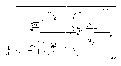
[0020] FIG. 1 is a schematic circuit diagram of an example embodiment of a
switching mode power amplifier as described herein.
[0021] FIG. lA is a schematic circuit diagram of an alternative embodiment
of the
switching mode power amplifier shown in FIG. 1.
[0022] FIG. 2 depicts an example modulation pulse train and resultant
integrated
signal having positive and negative components.
[0023] FIG. 3 is a time plot of an example input signal having zero voltage
crossing
points used to control switch timing of a portion of the circuit shown in FIG.
I.
[0024] FIG. 4 is a schematic flow chart describing an example method for
using the
switching mode power amplifier shown in FIG. 1.
DETAILED DESCRIPTION
[0025] Referring to the drawings, wherein like reference numbers refer to
like
components, a system 50 is depicted that includes a switching mode power
amplifier
device 10 and an example load 30 represented schematically as a resistor RL.
The power
amplifier device 10 is operable for amplifying a received modulated signal,
and for
ultimately powering the load 30 within the system 50 using energy released
from the
amplified modulated signal. The system 50 also includes a modulation circuit
16A, 16B
operable for receiving an input signal 40, e.g., information encoded as a
periodic or other
time-varying signal, modulating the received input signal 40 using a carrier
signal (arrow
C), and outputting separate first and second modulated voltage signals (Vm+,
Vm-) as
respective positive and negative voltage components. While shown as separate
elements
16A (MOD') and 16B (MOD-) to indicate separate processing of positive and
negative
cycles of a waveform defining the input signal 40, the modulation circuit 16A,
16B may
6
CA 02937821 2016-08-03
be embodied as a single integrated circuit outputting the separate first and
second
modulated voltage signals (Vm', Vm-) via different pins (not shown), as will
be
appreciated by one of ordinary skill in the art.
100261 Within the system 50 of FIG. 1, the power amplifier device 10
includes first
and second pairs of solid-state/semiconductor switches, i.e., a first
switching pair formed
respectively of a first and second semiconductor switch S1 and S2, and a
second
switching pair formed respectively of a third and fourth solid-state
semiconductor
switches S3 and S4, as well as a pair of transformers 18 formed from a first
and second
transformer Ti and T2 and a pair of steering diodes 19 formed from a
respective first and
second steering diode D1 and D2, all of which are described in further detail
below. FIG.
lA depicts alternative transformers 180 in an uncoupled inductor alternative
embodiment, with the battery 12 and input signal 40 omitted from FIG. lA for
simplicity.
Additionally, all switches Si, S2, S3, and S4 of FIG. 1A are depicted
schematically as
boxes to indicate that any combination of suitable semiconductor switches may
be used,
such as the IGBTs and MOSFETs of FIG. 1 or other configurations as set forth
herein.
A zero-crossing detection (ZCD) circuit 20 in the form of an integrated
circuit or other
suitable structure is also used as part of the power amplifier device 10,
receiving the input
signal 40 as an input voltage VIN and providing separate outputs ZC+ and ZC-
to
respective solid-state switches S3 and S4 of the type described below. In some
designs,
the modulation circuit 16A, 16B may be positioned separately from the power
amplifier
device 10 without departing from the intended inventive scope.
100271 With respect to the structure and intended function of each
component of the
power amplifier device 10 or the larger system 50 within which the power
amplifier
device 10 is used, a direct current (DC) battery (B) 12 may be embodied as a
multi-cell
battery of the type known in the art. The battery 12 has a calibrated DC
voltage output
level, e.g., approximately 120-150 VDC in an application-specific example
embodiment
in which the load 30 is a high-voltage transducer, e.g., for a sonobuoy or
other device.
As noted above, the modulation circuit 16A, 16B may be embodied as a single
integrated
chip or other circuit device although shown as separate elements for
illustrative clarity.
7
CA 02937821 2016-08-03
[0028] The modulation circuit 16A, 16B is operable for modulating the
received
input signal 40 using the carrier signal (arrow C), e.g., via application of a
periodic
triangle wave, a square pulse wave, or other typical periodic or repeating
modulation
waveform. The terms "modulation" and "modulating" as used herein refer to any
suitable ternary modulation technique, such as but not limited to pulse width
modulation
(PWM) or pulse density modulation (PDM). The term "ternary" as used herein
means
that the modulated signal has only three possible states, i.e., positive,
zero, and negative
voltage states. The modulation circuit 16A, 16B of FIG. I outputs the separate
first and
second modulated voltage signals (Vm+, Vm-), with a zero voltage crossing
between the
first and second modulated voltage signals (Vm+, Vm-) being automatically
detected via
operation of the zero-crossing detection circuit 20 and used in timing of the
power
switching control of the second pair of semiconductor switches S3 and S4 as
explained
below.
[0029] Referring briefly to FIG. 2, ternary modulation used herein can be
described
via the example use of center-sampled modulation pulses 25 shown as
progressively
wider modulation pulses numbered 1, 2, 3, and 4. A waveform 35 demarcated by
the
same pulse numbers 1, 2, 3, and 4 depicts an integrated voltage (V) delivered
over time
(t) by the successive modulation pulses 25, and also depicts the ternary
aspect of
modulation noted above, i.e., with separate positive (+), negative (-), and
zero (0) voltage
levels. The modulation circuit 16A, 16B of FIG. 1 separates the positive (+)
and negative
(-) components, which respectively correspond to the first and second
modulated voltage
signals (Vrvi+, Vm-) described above. The modulated voltage signal (Vm') is
then
delivered to the primary windings of the first transformer T1 of FIG. 1 while
the first
semiconductor switch Si is on/conducting. Similarly, the modulated voltage
signal (Vm-)
is delivered to the primary windings of the second transformer T2 of FIG. 1
when the
second semiconductor switch S2 is on/conducting.
[0030] The term "transformer" as used herein with reference to the example
first and
second transformers T1 and T2 refers to a set of primary and secondary
inductor
windings, whether configured as an optional coupled inductor as shown in FIG.
1 or as a
forward converter, or as an uncoupled inductor as shown in FIG. 1A. As is
known in the
8
CA 02937821 2016-08-03
art, coupled inductors such as flyback converters store electrical energy from
a power
source in a primary winding whenever a semiconductor switch supplying power to
the
coupled inductor is turned on/conducting, but does not transfer stored energy
to a
secondary winding until the same switch is turned off. In a forward converter
as typically
used in a distributed power architecture, energy is transferred from the
primary to the
secondary winding while the switch supplying the primary winding is
on/conducting. Of
the various types of transformers in use, coupled inductors are specifically
designed and
intended to store energy, and therefore may provide certain performance
advantages
when used within the system 50 depicted in FIG. 1. However, coupled inductors
are just
one possible way to implement the disclosure.
[0031] In one of the possible embodiments, energy can be stored via the
transformers
Ti and T2 only when electrical current flows in the primary windings of the
transformers
Ti and T2. With power defined as energy delivered per unit time, power
delivered to the
load 30 is thus dependent on the rapid transfer of energy through the power
amplifier
device 10. In other words, if electrical current can be pushed more quickly
through the
primary windings of the transformers T1 and T2 of FIG. 1, more energy is
ultimately
produced as a function of energy (E), inductance (L), and electrical current
(i), with this
function represented mathematically as E = Li2
2
[0032] As will be appreciated by those of ordinary skill in the art, the
equation noted
above is a solution to an integral, and thus establishes that an inductor acts
an integrator
of current. The integration time is much longer than the transition time of a
semiconductor switch. That is, voltage across an inductor is expressed as V=L
di . The
dt
increase of energy over time is expressed as dE (joules) = Lidi. Thus, the
energy stored
in an inductor is expressed as E = dE = L f idi = ¨1 LI 2, with the time
associated with
2
0
overall switching function being a function of inductor switching. This in
turn illustrates
the linearity benefit of the present approach, as the ratio of the
semiconductor transition
time to the inductor current integration time is a very small number, and
therefore
9
CA 02937821 2016-08-03
contributes very little to distortion. In addition, at low power, in a PWM
system small
pulse widths are needed, with wider pulse widths needed at high power. This
means that
static losses accumulate only as a function of power storage. The fact the
load is isolated
during this interval means that the only load during the charge interval is
the inductor
current.
100331 The power amplifier device 10 of FIG. 1 is thus scalable to larger
or smaller
loads 30, with isolation of the load 30 provided in two different manners: via
switching
isolation due to the control of the second set of switches S3 and S4 only at
the zero-
crossing of the input signal 40, and via low levels of leakage inductance
provided by the
transformers Ti and T2.
[0034] Referring again to FIG. 1, the switches Si and S2 respectively
receive the
corresponding voltage signals Vm1 and Vm-, and then transfer the voltage
signals Vm+ and
Vm- to the respective first and second transformers Ti and T2. The
semiconductor
switches S3 and S4 are electrically connected to an output side of the first
and second
transformers Ti and T2, respectively, and thus are powered by the transformers
Ti and
T2 according to a particular switching control sequence as set forth below
with reference
to FIG. 4. The diode D1 in this embodiment is serially connected, i.e.,
connected in
electrical series, between the first transformer T1 and the third
semiconductor switch S3,
while the diode D2 is serially connected between transformer T2 and the fourth
semiconductor switch S4.
[0035] In the example embodiment as shown in FIG. 1, the first pair of
semiconductor switches Si, S2 may be optionally embodied in a non-limiting
application
as metal-oxide semiconductor field effect transistors (MOSFETs) of the type
known in
the art, with the second pair of semiconductor switches S3, S4 may be
optionally
embodied as insulated gate bipolar transistors (IGBTs). As is known in the
art, IGBTs
have designated gate (G), emitter (E), and collector (C), each of which is
labeled as such
in FIG. 1. However, other solid-state switch configurations may be used
depending on
the intended application, including using only MOSFETs, only IGBTs, or using
other
gate-controlled solid-state switches. For instance, high electron mobility
transistors
(HEMTs) using gallium nitride (GaN) or other suitable materials may be used in
lieu of
CA 02937821 2016-08-03
MOSFETS and IGHTs. In general, the switching rate and thus the design of the
first pair
of semiconductor switches Sl, S2 depends on the modulation encoding scheme
used by
the modulation circuit 16A, 16B.
[0036] As a design consideration, within the scope of the present
disclosure the first
pair of semiconductor switches Sl, S2 has a high switching speed requirement
in that the
first pair of semiconductor switches Sl, S2 must always switch at the or above
the
frequency of the carrier (C), i.e., the carrier frequency. By contrast, the
switches of the
second pair of semiconductor switches S3, S4 change their respective switching
states at
a substantially slower rate than that of the first pair of semiconductor
switches Si, S2,
i.e., switching only at the zero-crossing rate of the input signal 40, with
the carrier
frequency expected herein to be substantially higher than the zero-crossing
rate.
[0037] To illustrate the latter point, FIG. 3 depicts the input signal 40
as a time-
varying signal, i.e., having a voltage magnitude V; that changes over time
(t). The input
signal 40 has positive (+) and negative (-) components as shown. The input
signal 40
crosses through zero volts whenever the input signal 40 changes its sign, with
each zero-
crossing demarcated in FIG. 3 by a corresponding zero-crossing point 42. The
zero-
crossing detection circuit 20 of FIG. 1, for instance an operational amplifier
or other
suitable comparator circuit or other integrated circuit, detects each zero-
crossing point 42
and, in response to such detection, activates a designated one of the third or
fourth
semiconductor switches S3 or S4 and simultaneously deactivates the other
semiconductor
switch S3 or S4 in the same pair, with the identity of the activated switch
changing with
the detection of each successive zero-crossing point 42.
[0038] That is, when the third semiconductor switch S3 of FIG. 1 is
actively
conducting, the fourth semiconductor switch S4 is not conducting, and vice
versa. In this
manner, the switching function of the first pair of semiconductor switches Si,
S2 is
temporally separated from any downstream switching used to deliver stored
energy from
the transformers Ti or T2 to the load 30, i.e., the switching function in the
switching
mode power amplifier device 10 is isolated from its load function via targeted
low-
frequency/zero-crossing control of the second pair of semiconductor switches
S3, S4 and
diodes DI, D2.
11
CA 02937821 2016-08-03
100391 As part of the power amplifier device 10, the steering diodes D1 and
D2 direct
the energy released by the transformers Ti, T2 to the second pair of switches
S3, S4. The
diodes D1, D2 are thus an important part of the load isolation functionality
enabled by the
present disclosure, and for that reason should be constructed from materials
of
sufficiently high-speed and high-energy density, such as silicon carbide,
gallium nitride,
or other high-mobility semiconductor materials. With respect to the
transformers Ti and
T2 of FIG. 1, these devices may be embodied as suitable energy storage
devices, such as
those having a linear output as a function of pulse density or pulse width. In
the
embodiment of FIG. 1, energy is stored in the primary winding of each of the
transformers T1 and T2 when the corresponding semiconductor switch S1 or S2 is
on/conducting, and is transferred to the secondary winding only when the
corresponding
semiconductor switch Si or S2 is turned off, i.e., is not conducting.
100401 The transformers Ti, T2 should be constructed in such a manner as to
provide
high-quality inductive coupling between the primary and secondary windings and
thereby
provide low levels of leakage inductance. As used herein, "low leakage
inductance"
refers to levels of less than about 1/80th to 1/100th of a primary inductance
of the primary
windings. In another optional embodiment, the primary and secondary windings
of each
of the transformers Ti and T2 may be concentrically wound, i.e., the primary
winding of
the first transformer Ti is wound concentrically with the secondary winding of
the
second transformer Tl, with the same arrangement in the second transformer T2.
Additionally, the transformers T1 and T2 are electrically connected in reverse
polarity
with respect to each other.
[0041] The identity of the load 30 shown schematically in FIG. 1 may vary
with the
particular application. In general, in order to benefit fully from the present
disclosure, the
load 30 may be a high impedance reactive load having a power factor not
exceeding 0.65
for high-power applications. Example embodiments of the load 30 may include a
transducer, an antenna, an audio speaker, or an electric motor. In a
particular
embodiment, the load 30 may be a sonobuoy transducer used as part of a
sonobuoy
assembly, for instance to deploy or actuate directional hydrophones or other
aquatic
12
CA 02937821 2016-08-03
acoustic sensors and/or signal transmitters, without in any way limiting
applications to
such a field of art.
100421 Referring to FIG. 4, an example embodiment of the method 100 begins
with
step S102, which may be executed offboard with respect to the remaining steps
of the
method 100. At step S102, the input signal 40 of FIG. 1 is modulated. The
input signal
40 may be transmitted from a remote location such as a transmission tower or
antenna
and communicated to the modulation circuit 16A, 16B as is well known in the
art. The
modulation circuit 16A, 16B itself may be separate from the switching mode
power
amplifier device 10. Step S102 may entail modulating the input signal 40 via a
carrier
signal (arrow C) using ternary PWM, ternary PDM, or other conventional ternary
modulation techniques, doing so via operation of the modulation circuit 16A,
16B of FIG.
1. The method 100 proceeds to step S104 once the input signal 40 has been
modulated.
100431 At step Si 04, the modulated signal that is output by the modulation
circuit
16A, 16B is separated into its positive and negative voltage components (Vm',
Vm-) as
shown in FIG. 2. In practice, the modulation circuit 16A, 16B may be designed
to output
separate positive and negative voltage components (Vivi', VM) as opposed to
separating a
modulated signal into the different components. The positive voltage component
(Vm+)
is then electrically conducted or transmitted to the gate (G) of the first
semiconductor
switch Si shown in FIG. 1. Likewise, the negative voltage component (W) is
delivered
to the gate (G) of the second semiconductor switch S2. The method 100 then
proceeds to
step S106.
100441 Step S106 entails switching the first set of semiconductor switches
Si, S2 at a
rate that is equal to or greater than the carrier frequency ( fc). For
example, if the carrier
frequency is 30-40 kHz, the switching frequency of the first pair of
semiconductor
switches SI, S2 may be at least 30-40 kHz, or approximately 350-400 kHz or
about 10
times the carrier frequency in other embodiments. Only when the first or
second
semiconductor switch S1 or S2 is commanded to an on/conducting state will
energy be
stored in the primary windings of the transformers Ti or T2, respectively. The
method
100 then proceeds to step S108.
13
CA 02937821 2016-08-03
[0045] Step S108 entails detecting a zero voltage crossing of the input
signal 40 via
the zero-crossing detector 20 of FIG. 1, with example zero-crossing points 42
depicted in
FIG. 3. Step S108 may include using an operational amplifier or other suitable
comparator circuit to detect the zero voltage crossing. The method 100
proceeds to step
S110 when a zero voltage crossing is not detected, and to step S112 when a
zero voltage
crossing is detected.
[0046] At step S110, the present switching state of the second pair of
semiconductor
switches S3, S4 is maintained, i.e., not changed. For instance, if the third
semiconductor
switch S3 is on/conducting and the fourth semiconductor switch S4 is off/not
conducting,
then switch S3 remains on and switch S4 remains off. The method 100 proceeds
to step
S114.
100471 Step S112 includes changing the switching state of the semiconductor
switches S3, S4 from a state that existed just prior to the detection of a
zero voltage
crossing at step S110. For example, if the third semiconductor switch S3 was
on/conducting and the fourth semiconductor switch S4 was off/not conducting,
the
detection of a zero voltage crossing at step S108 results in the third
semiconductor switch
S3 turning off and the fourth semiconductor switch S4 turning on, for instance
via a
change of voltage delivered to the gates (G) shown in FIG. 1. The method 100
then
proceeds to step S114.
[0048] At step S114, electrical power or energy is delivered to the load 30
through
the on/conducting semiconductor switch S3 or S4, whichever of the two is in a
conducting state.
[0049] As set forth above, the power amplifier device 10 provides for
signal
conversion and amplification via the use of the transformers TI, T2 and
targeted low-
frequency switching control of the second pair of semiconductor switches S3,
S4
downstream of the transformers Ti, T2. This occurs only at detected zero
voltage
crossing points of an input signal, such as the zero voltage crossing points
42 and input
signal 40 of FIG. 3, to allow the load 30 and its associated impedance to be
isolated from
the high-speed switching function of the first pair of semiconductor switches
Sl, S2. As
a result, the first pair of semiconductor switches Sl, S2 is able to work more
efficiently
14
CA 02937821 2016-08-03
than would ordinarily occur in existing designs, with gains of 30% in
efficiency or more
being possible relative to the typical efficiency levels available via the
conventional art.
Also, the power amplifier device 10 allows for a fully scalable power output,
with the
high-efficiency control technique of the method 100 minimizing internal
dissipation of
heat within the power amplifier device 10. Such benefits may be desirable in
many
applications, including but not limited to transducer systems of the type used
for coupling
acoustic pulse energy into water, e.g., sonobuoy applications, audio
applications in which
modulated waves are transmitted to an antenna for playback via a set of
speakers, and the
like.
100501 The detailed description and drawings are supportive and descriptive
of the
disclosure, but the scope of the invention is defined solely by the claims.
While some of
the best modes and other embodiments for carrying out the disclosure have been
described in detail, various alternative designs and embodiments exist for
practicing the
disclosure as defined in the appended claims.