Note: Descriptions are shown in the official language in which they were submitted.
CA 02938483 2016-08-15
1
Device for converting radiofrequency energy into DC current (rectifier
antenna) and corresponding
sensor
1. Field of the invention
The field of the invention is that of the harvesting (retrieval) of energy.
More specifically, the invention relates to a technique for converting radio-
frequency energy
into DC current or into DC voltage in order to power, for example, electronic
circuits.
The invention can be applied especially in the field of power supplies for
wired or wireless
sensors, for example, in the field of textiles (sensors carried on clothing),
medicine (biomedical implants,
cardiac stimulators, thermometers, etc.), weather forecasting (remote weather
stations, thermometers,
etc.), sports (heart rate meters, acceleration meters, oxygen meters, etc.),
radio-frequency identification
(RFID), mobile telephony (battery recharging, etc.), monitoring, etc.
2. Prior art
Lower power consumption by electronic components has led to an increase in
mobile
applications such as wireless sensors. Most of these sensors or wireless
sensor networks (WSN), such as
those carried by individuals (known as body sensor area networks or BSANs),
are powered by
cells/batteries. RFID wireless sensors which are most commonly used consume
tens of microwatts in
sleep mode and several hundreds of microwatts in active mode.
Even if major progress has been seen in recent years, batteries still have a
limited service life
and using them raises problems in terms of their accessibility and constraints
on their volume (especially
for subcutaneous medical implants).
It is therefore sought to explore other alternatives to power these sensors,
for example by
harvesting the energy available in the surrounding environment. Thus, heat
gradients, mechanical
vibrations, light waves or radio-frequency waves especially are potential
sources of energy for powering
these sensors.
In particular, radio-frequency sources have the advantage of being present
everywhere in daily
life, especially in urban surroundings. Indeed, a multitude of wireless
communications standards has led
to the proliferation of radio transmitters such as GSM (900 MHz, 1800 MHz),
UMTS (2.1 GHz) and WiFi
(2.4 GHz) transmitters. These radio-frequency energies, transmitted
continuously by
telecommunications networks, are therefore being made available on a wide
range of frequencies.
The purpose of radio-frequency energy harvesting is to convert the energy
coming from ambient
radio-frequency sources into DC voltage and DC current. The basic element that
ensures this conversion
is called a RF-DC converter, a rectifying antenna or again a rectenna.
CA 02938483 2016-08-15
2
Figure 1 is thus a schematic drawing of a radio-frequency energy harvesting
device.
According to this schematic drawing, radio-frequency waves 11 are received by
a reception
antenna 12 and then converted into DC voltage and DC current by an RF-DC
converter 13. The current
thus generated can be used to power a load 14 which represents, for example, a
sensor to be powered.
More specifically, the RF-DC converter 13 comprises an input filter 131, also
called a radio-
frequency (RF) filter or a high frequency (HF) filter, a rectifier 132 and an
output filter 133, also called a
DC filter. The input filter 131 is placed between the reception antenna 12 and
the rectifier 132. This is a
low-pass filter used to block undesirable harmonics. Several types of
rectifiers can be envisaged
depending chiefly on the incident power and the frequency. In order make the
right choice of topology,
a compromise must be obtained between the output load voltage and the
conversion efficiency, as
described in the document "A multi-tone RF energy harvester in body sensor
area network context" by
V.Kuhn, F.Seguin, C.Lahuec and C.Person, IEEE LAPC conference, Loughborough,
November 2013.
Several types of RF-DC converters have been proposed, adapted to receiving
radio-frequency
energy on one or more frequency bands.
Thus, especially radio-frequency energy harvesting circuits have been proposed
for harvesting
the radio-frequency energy transmitted on a single frequency band, by using a
single rectenna.
It can be noted however that the function of such a rectenna is considerably
impaired if the
operating frequency has been modified relative to the optimal resonance
frequency. Thus, one
drawback of these circuits for harvesting radio-frequency energy transmitted
in a single frequency band,
implementing a single rectenna, is that they are not suited to the ambient
environment in which the
predominant frequencies differ according to the place of use of the load (for
example according to the
place of the sensor).
Circuits have also been proposed for harvesting radio-frequency energy
transmitted in several
frequency bands. Indeed, it has been shown especially that when several
sources of radio-frequency
energy emitting in different frequency bands are available in the surrounding
environment, the quantity
of energy harvested can be increased. Thus, as shown in figure 2, rectenna
networks have been
proposed wherein several rectennas (working at different frequencies) are
placed in parallel. The DC
outputs of each rectenna are added 15 to one another so as to increase the
power harvested.
One drawback of these circuits for harvesting radio-frequency energy
transmitted in several
frequency bands, implementing several rectennas in parallel, is that they
require a summing of the DC
voltages contributed by each frequency band. Now, if this summing is not
properly done it can
drastically impair the efficiency of the circuit.
3
Several techniques have been proposed to implement this kind of summing of the
DC voltages,
using serial or differential topologies of interconnection.
The serial association of rectifiers to achieve the summing, according to a
first structure
illustrated in figure 3A, can give RF/DC conversion efficiency greater than
that of a single frequency band
circuit. This is possible only if each arm of the structure is operating, i.e.
if the radio-frequency signals
are received and processed on each arm of the structure. Indeed, if one of the
frequencies is not present
in the dedicated arm, this arm is seen as a load for the rest of the circuit.
It thus impairs the overall
performance of the circuit.
The use of Greinacher-type rectifiers to carry out the summing, according to a
second structure
illustrated in figure 3B, makes it possible to add up the DC outputs without
any interference between
these different outputs. Indeed, the output of each rectifier is differential.
By contrast, one drawback
of such a structure is that it requires minimum incident power of -10 dBm for
an architecture
implementing two Greinacher-type rectifiers. Now, in an urban environment, the
average power
density of the frequency bands is lower, i.e. lower than -10 dBm. Thus, this
type of architecture is not
suited to converting energy coming from ambient radio-frequency sources into
DC current for the
powering of loads.
There is therefore a need for a novel circuit for harvesting radio-frequency
energy transmitted in
one or more frequency bands that does not have these drawbacks of the prior
art.
3. Summary of the invention
The invention proposes a novel solution that does not have all these drawbacks
of the prior art
in the form of a device for converting radio-frequency energy into DC current,
receiving at least one
radio-frequency signal at input and generating at output a DC current capable
of powering at least one
load.
According to the invention, such a conversion device comprises at least two
conversion stages,
each comprising:
- a radio-frequency filtering module, connected to a first input node of said
conversion stage,
configured to filter one of said at least one radio-frequency signal;
- a voltage shift module, connected between a second input node of said
conversion stage, said
radio-frequency filtering module and an intermediate node of said conversion
stage, configured
to shift a voltage present at said first input node to said intermediate node;
- a voltage rectifier module, connected between said intermediate node, said
second input node
and an output node of said conversion stage, configured to rectify the voltage
of said
Date Recue/Date Received 2021-05-06
CA 02938483 2016-08-15
4
intermediate node and deliver a rectified voltage on said output node.
In addition, for the first conversion stage, the second input node is
connected to a reference
voltage and, for a higher conversion stage (second, third, etc.), the second
input node is connected to
the output node of a lower conversion stage.
Finally, the DC current is generated on the output node of the last conversion
stage.
The invention thus proposes a novel device for harvesting radio-frequency
energy, used
especially to power electronic devices such as sensors.
In particular, the conversion device of the invention comprises several
conversion stages. It is
adapted to harvesting the radio-frequency energy transmitted in a single
frequency band, by activating a
single conversion stage (or if a single conversion stage is available), and to
harvesting the radio-
frequency energy transmitted in several frequency bands by activating several
conversion stages, one
per frequency band. It can be noted that the number of conversion stages is
not limited.
When several conversion stages are activated the proposed conversion device
makes it possible
especially to provide for efficient summing of the DC voltages contributed by
each frequency band
present. In particular, the proposed structure enables the adding up of the DC
outputs of each
conversion stage without any interference between these outputs, even when
certain stages are not
active, i.e. when these stages do not receive any radio-frequency signal.
In addition, the conversion device according to the invention requires lower
incident power than
do the prior art devices in order to be able to generate a DC current (or in
an equivalent way, DC
voltage) capable of powering of at least one load.
According to one particular embodiment of the invention, the voltage shift
module uses a first
capacitor, connected between the filtering module and the intermediate node,
and a first diode,
forwardly connected between the second input node and the intermediate node.
The voltage rectifier
module implements a second capacitor, connected between the second input node
and the output
node, and a second diode, forwardly connected between the intermediate node
and the output node.
Thus, each conversion stage implements two inverse-parallel-connected diodes.
Hence, to be
able to generate a DC current capable of powering at least one load, it is
enough to have available
power sufficient to cross the threshold of one diode. By way of a comparison,
the use of Greinacher-
type rectifiers to harvest the radio-frequency energy transmitted in several
frequency bands relies on
the use of several series-connected diodes, requiring far greater incident
power to start the circuit.
The conversion device according to the invention therefore works with lower
incident power
values than do the prior art devices.
CA 02938483 2016-08-15
In addition, the conversion device according to the invention
relies on the use of half
as many components as those used in the prior art devices, thus entailing
lower production costs.
According to one particular aspect of the invention, the components (diodes
and capacitors) are
surface-mounted components (SMCs). A device for converting energy according to
the invention is
5 therefore easy to make and/or easy to detect.
According to one variant, these components can be integrated components.
Such a conversion device therefore takes the form of an electronic circuit
which can be printed,
integrated, etc.
According to another particular characteristic of the invention, the first and
second diodes have
approximately identical values.
Thus, within the same conversion stage, the two inverse-parallel-connected
diodes have roughly
identical threshold voltages. This gives a symmetry at the level of a
conversion stage, optimizing the
rectification.
According to one variant, the diodes within a same conversion stage, or within
different
conversations stages, have different threshold voltages.
For example, the first and second diodes are Schottky diodes.
Such diodes used prevent the appearance of parasitic or unwanted capacitances.
Naturally, any
type of diode having a low threshold voltage can be used (for example a PN
junction diode, etc.).
According to one particular characteristic of the invention, the conversion
device comprises at
least one reception antenna for receiving the radio-frequency signal or
signals.
Such a device can indeed be used to harvest the radio-frequency energy
conveyed in the
ambient air.
For example, the conversion device comprises a single wide-band reception
antenna.
Thus, the invention provides a more compact structure which is nevertheless
adapted to the
reception of radio-frequency signals available in several frequency bands.
According to one variant, the reception device comprises a distinct reception
antenna for each
conversion stage, each reception antenna being adapted to receiving a radio-
frequency signal in a given
frequency band. In this case, each reception antenna can have a narrow band.
For example, the radio-frequency filtering module comprises a radio-frequency
filter belonging
to the group comprising:
- a bandpass filter centered on the 900 MHz frequency;
- a bandpass filter centered on the 1800MHz frequency;
CA 02938483 2016-08-15
6
- a bandpass filter centered on the 2.1GHz frequency;
- a bandpass filter centered on the 2.4GHz frequency.
Such a conversion device is thus suited to receiving the GSM 900 MHz and/or
GSM 1800 MHz
and/or UMTS and/or WiFi frequency bands.
Naturally, other frequency bands (from very low frequencies to very high
frequencies) can be
listened to in order to harvest radio-frequency energy from one or more radio-
frequency signals.
According to another embodiment of the invention, the radio-frequency signal
or signals are
received via a wired link.
The presence of reception antennas is therefore optional. In this case, the
radio-frequency signal
or signals can be picked up directly at source. For example the source can be
a decoding box of the
Livebox (registered mark) type. The energy conversion device according to the
invention can be directly
connected to this decoding box by a wired link.
The invention also relates to a sensor comprising means for collecting data
and means for
rendering collected data. According to the invention, such a sensor also has a
device for converting
radio-frequency energy into DC current as described above, receiving at input
at least one radio-
frequency signal and generating at output DC current powering this sensor.
Such a sensor could of course comprise the different characteristics of the
device for converting
radio-frequency energy into DC current according to the invention. These
characteristics can be
combined or taken in isolation. Thus, the characteristics and advantages of
this sensor are the same as
those of the conversion device and are not described in greater detail.
4. List of figures
Other characteristics and advantages of the invention shall appear more
clearly from the
following description of a particular embodiment, given by way of a simple
illustratory and non-
exhaustive example, and from the appended drawings, of which:
- Figure 1, described with reference to the prior art, presents a schematic
drawing of a device for
harvesting radio-frequency energy;
Figure 2, also described with reference to the prior art, illustrates the
harvesting of energy on
several frequency bands;
- Figures 3A and 3B present two examples of RF-DC converters used to
harvest energy on several
frequency bands according to the prior art;
- Figure 4 illustrates the general principle of a device for converting
radio-frequency energy into
DC current according to the invention;
CA 02938483 2016-08-15
7
- Figures 5 and 6 present two examples of conversion devices for
converting radio-frequency
energy according one embodiment of the invention;
- Figures 7 and 8 illustrate the performance values of the invention;
- Figure 9 illustrates an example of a sensor powered by a device for
converting radio-frequency
energy into DC current according to one embodiment of the invention.
5. Description of one embodiment of the invention
5.1 General principle of the invention
The general principle of the invention relies on a novel device for converting
radio-frequency
energy into DC current (and in an equivalent way into direct voltage),
receiving at input at least one
radio-frequency signal and generating at output DC current capable of powering
at least one load.
The particular structure of the device according to the invention is used
especially to harvest the
radio-frequency energy present on one or more frequency bands and to provide
for an efficient
summing of the DC voltages when radio-frequency energy is harvested on several
frequency bands.
In particular, the proposed device is formed by one or more conversion stages
each capable of
processing a radio-frequency signal received on a distinct frequency band. The
differential output of
each conversion stage enables a lossless summing of the DC voltages generated.
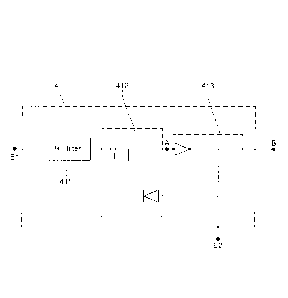
Figure 4 more specifically illustrates the general principle of a conversion
device according to the
invention, in the form of an electronic circuit.
Such a conversion device comprises at least two conversion stages 41 each
comprising:
- a radio-frequency filtering module 411, connected to a first input node El
of the conversion
stage 41, configured to filter a radio-frequency signal. Such a filtering
module 411 comprises for
example a bandpass filter centered on the frequency Fl. It is used to transmit
maximum power
to the rest of the circuit in the desired frequency band and to block
undesirable harmonics to
enable optimal conversion efficiency.
- a voltage shift module 412 connected between a second input node E2 of the
conversion stage
41, the radio-frequency filtering module 411 and an intermediate node A,
configured to shift a
voltage present in the first input node El to the intermediate node A of the
conversion stage 41;
- a voltage rectifier module 413 connected between the intermediate node A,
the second input
node E2 and an output node B configured to rectify the voltage of the
intermediate node A and
to deliver a rectified voltage at the output node B of the conversion stage
41.
In particular, it can be noted that the second input node E2 is connected
either to a reference
voltage or to the output node of another conversion stage.
CA 02938483 2016-08-15
8
When the device has several conversion stages, the second input node E2 of the
first stage
is connected to a reference voltage, for example to ground or to a 1V
reference, and the second input
nodes E2 of the other stages are connected to the output nodes B of the lower
stages (the second input
node of the second stage is connected to the output node of the first stage,
the second input node of
the i-th stage is connected to the output node of the (i-1)-th stage, etc).
In addition, the DC current capable of powering at least one load is generated
at the output
node B of the conversion stage if this output node is not connected to a
second input node of another
conversion stage. In other words, the DC current is generated on the output
node of a conversion stage
that is not connected to a second input node of another conversion stage.
Figure 5 illustrates the architecture of the proposed solution for a
conversion device comprising i
conversion stages referenced 51, 52 and Si.
Each conversion stage is formed by a filtering module, a voltage shift module
and a voltage
rectifier module as described above.
The conversion device illustrated in figure 5 is used to generate DC current
lx used to power a
load RL, connected between the output node Bi of the i-th conversion stage 5i
and the second input
node E2(51) of the first conversion stage 51, which is connected to ground.
More specifically, the first conversion stage 51 comprises two input nodes
El(51) and E2(51),
one intermediate node Al and one output node 81. The second input node E2(51)
is connected to a
reference voltage, for example ground. This first conversion stage 51
comprises a first filtering module
511, centered on the frequency Fl. If Vro denotes the AC voltage induced at
the first input node
El(51), at input of the filtering module 511, then the voltage shift module,
comprising the first capacitor
C1,1 and the first diode D1,1, shifts the voltage Vti to the intermediate node
Al. Thereafter, the
voltage rectifier module, comprising the first capacitor C2,1 and the second
diode D2,1, rectifies the
voltage at the intermediate node Al to obtain a DC voltage at the output node
Bl, denoted Vouti.
The second conversion stage 52 comprises two input nodes El(52) and E2(52),
one intermediate
node A2 and one output node 82. The second input node E2(52) is connected to
the output node B1 of
the first conversion stage 51. This second conversion stage 52 comprises a
second filtering module 521
centered on the frequency F2. If Vrt2 denotes the AC voltage induced at the
first input node E1(52), at
input of the filtering module 521, then the voltage shift module, comprising
the first capacitor C1,2 and
the first diode D1,2, shifts the voltage Vrf,2 to the intermediate node A2.
Thereafter, the voltage
CA 02938483 2016-08-15
9
rectifier module, comprising the second capacitor C2,2 and the second diode
D2,2, rectifies the
voltage at the intermediate node A2 to obtain a DC voltage at the output node
B2 denoted V0ut2.
The i-th conversion stage 5i comprises two input nodes E1(5i) and E2(51), one
intermediate node
Ai and one output node Bi. The second input node E2(5i) is connected to the
output node B(i-1) of the
conversion stage (i-1). This i-th conversion stage 5i comprises an i-th
filtering module 5i1 centered on
the frequency Fl. If Vrtj denotes the AC voltage induced at the first input
node E1(5i), at the input of the
filtering module 511, then the voltage shift module, comprising the first
capacitor C1,i and the first diode
D1,i, shifts the voltage Vrtj to the intermediate node Ai. Thereafter, the
voltage rectifier module,
comprising the second capacitor C2,i and the second diode D2,i, rectifies the
voltage at the intermediate
node Ai to obtain a DC voltage at the output node Bi, denoted as V0uti.
According to the proposed example, the first conversion stage 51 is referenced
to ground
(second input node E2(51) connected to ground) and the i-th conversion stage
Si is referenced relative
to the (i-1)-th conversion stage (second input node E2(5i) connected to the
output node of the
conversion stage (i-1)).
Each conversion stage therefore forms a rectifier antenna or rectenna.
It can be noted that the first input nodes E1(51), E1(52), E1(5i) of each
conversion stage can
each be connected to one distinct reception antenna, capable of receiving a
radio-frequency signal in
the frequency band associated with the conversion stage considered. As a
variant, the first input nodes
E1(51), E1(52), E1(51) of each conversion stage can be connected to a single
antenna, for example to a
wide-band antenna, capable of receiving radio-frequency signals in frequency
bands associated with the
different conversion stages. It is thus possible to define a structure more
compact than a structure that
relies on the use of several "directional" reception antennas each adapted to
one specific frequency
band. According to yet another variant, the first input nodes E1(51), E1(52),
E1(5i) are directly
connected (by wired links for example) to one or more sources generating a
radio-frequency signal.
In particular, it can be noted that if one or more conversion stages are not
powered by a voltage
Vrti, these stages will not disturb the other conversion stages powered by a
voltage Vri through the
differential output Vouti of each conversion stage and second capacitors C2i
which maintain the DC
level.
The DC current 'DC is generated on the output node Bi of the conversion stage
i, since the output
node Bi is not connected to a second input node of another conversion stage.
The total voltage obtained
CA 02938483 2016-08-15
VDc is the sum of the contributions V0u0 of the different conversion stages,
as shown below.
The technical solution proposed therefore provides for a wide-band system and
enables the
addition of the DC voltages obtained for each frequency band without loss of
voltage at output, with a
low incident power of the order of -30 dBm. Indeed, the invention requires
half as many diodes as in
5 the case of a Greinacher-type rectifier. In addition, it must be noted
that the number of frequency
bands, i.e. the number of conversion stages is not limited.
5.2 Analytic expression of the proposed solution
Here below, the analytic expression of the proposed solution is presented.
This analytic
expression is used especially to show that the total voltage obtained Vric is
the sum of the contributions
10 Vout, of the different conversion stages.
To this end, each conversion stage is considered to be formed by a filtering
module, a voltage
shift module comprising a first capacitor and a first diode, and a voltage
rectifier module comprising a
second capacitor and a second diode.
It is assumed that the capacitors of the conversion device are perfect and
that their operation is
ideal: they let through radio-frequency signals and block DC current.
It is also assumed that the diodes of the same stage have similar threshold
voltages and are
Schottky-type diodes, modeled by an exponential relationship.
The current /din the diodes is then written as:
(t/cliode 1.))
Id = exp _________ (1)
with:
/ a constant specific to the type of diode considered;
V the threshold voltage of the diode considered;
Vdtode the voltage at the terminals of the diode considered.
In the equation (1), the term Vthode represents the voltage at the terminals
of each diode which
can be written as follows:
Vdiode = Vapplied Vrf = Vappued IVrf Icos(wt) (2)
The voltage Vap p lied applied to the diode in taking account of the series
resistance Rs of the
CA 02938483 2016-08-15
11
diode can be expressed as follows:
Vapplied = Vpola RSIDC (3).
It is assumed that the capacitances Ci act as decoupling capacitances: they
prevent the DC
current from circulating and have little effect on the incident wave of
amplitude Vff,i present at the input
of each conversion stage, also called an input voltage.
If all the diodes are identical, their static bias Vpolo is computed as a
function of the DC voltage
of the previous conversion stage.
We thus have:
1
V =¨'(V ¨V
polo 2 out j-1 out ,i) (4)
V = ¨V ¨ R I + V cos(at) (5)
diode out s DC rf
The computation of the current flowing through each diode can be done through
the Bessel
functions which enable the development of the exponential term:
exp(xcos(cot))=E30(x)+2IB,(x)cos(nwt) (6)
Thus, it is possible to isolate the direct term of the current flowing through
the diodes:
(exp( Vdiode,i
= 1))
VT
olcosn
1
Id = I VT s(exp (Vapplied)exp
VT )
v
= i (exp (V)aPP/ted) (B0 f r' ) + 2 EB (1.771) cos(a0) ¨ 1) (7)
vT v
Thus we have:
'DC = Is (exp (V apptted) B0 (11771,1 (8)
VT VT
Moreover, the following approximate function can be used for B0:
exp(x)
(x)= _________________ (9)
\/27-rx
We thus obtain the following expression for the current IDc:
CA 02938483 2016-08-15
12
ex p( _________________________ '
'DC exp (v"P"ed) v (10)
12 al lir"'
VT /
The equation (10) gives a relationship between the point of bias at output of
the conversion
device and the amplitudes of the incident voltages 11,_ :
( V
In 277- ____________ if,'
V VT ) I ) V RI
rf
______________________ +Ini DC P0,, 0 s DC (11)
VT 2 I ) VT VT
Thus:
( V,
yin 27r _______________
VT (I
T1111 CLI j ¨ ¨V V (12)
1
V = V (,
2 , out,i)+ R si DC
rf,i 2
whence:
Vf
V InL27r
V . (V R V 1 T VT
Out,' +V out) 4_ 5 out, =-+ Vrf (13)
2 7" R11) 2 out ,11
2
s
The equation (13) is the analytic expression that describes the behavior of
the conversion
device. Indeed, it relates the parameters of the diode and the output DC
voltage V0ut,1_1 to the
amplitude of the input voltage V1. of the i-th conversion stage. This
expression confirms that the DC
outputs of the different conversion stages (i.e. the different rectennas) are
correctly summed.
5.3 Results of simulation
The implementing of conversion devices comprising either one conversion stage
or two
conversion stages or three conversion stages has been simulated. The following
table presents the
voltages applied at input/obtained at output at the different nodes of the
conversion device, on the
basis of the notations of figure 5:
Number of
Vrf,1 (V) Vrf,2 (V) Vrf,3 (V) Vout,1 (V)
Vout,2 (V) Vout,3 (V) Vcc (V)
stages
1 0.65 0.86 0.86
CA 02938483 2016-08-15
13
2 0.6 0.6 0.75 0.73 1.475
3 0.55 0.55 0.55 0.5 0.8 0.6 1.9
It can be seen that for a conversion device comprising two conversion stages
each powered by
the same input voltage (Vrf,1 = Vrf,2) the total output voltage VDc is twice
as great as the output voltage
of the first conversion stage Vouto..
Figure 6 more specifically illustrates an example of an electrical circuit for
the simulation of the
conversion of radio-frequency energy conveyed in two distinct frequency bands.
The device for
converting radio-frequency energy into DC current illustrated in figure 6
therefore comprises two
conversion stages. For example, the first conversion stage 61 comprises a
radio-frequency filter 611
centered on the 0.9 GHz frequency, enabling the harvesting of energy emitted
in the GSM900 band, a
voltage shift module 612, comprising a first capacitor C1,1 and a first diode
D1,1, and a voltage rectifier
module 613, comprising a second capacitor C2,1 and a second diode D2,1. The
second conversion stage
62 comprises a radio-frequency filter 621 centered on the 2.1 GHz frequency,
used to harvest energy
emitted in the UMTS 2100 band, a voltage shift module 622, comprising a first
capacitor C1,2 and a first
diode D1,2, and a voltage rectifier module 623, comprising a second capacitor
C2,2 and a second diode
D2,2. The values of the diodes and the capacitors can be chosen as a function
of the load to be
powered. For example, the diodes D1,1, D2,1, D2,1 and D2,2 have a threshold
voltage of the order of
150 mV and the capacitors have a value of the order of 15 pF for the first
capacitors C1,1 and C1,2 and
68 pF for the second capacitors C2,1 and C2,2.
Figure 7 illustrates the output voltage VDc obtained at output of the
conversion device of figure
6 as a function of the incident power Pin when:
- only the
first conversion stage 61 is activated (i.e. when a radio-frequency signal is
received only
in the frequency band around the 0.9 GHz center frequency), curve 71:
- only the second conversion stage 62 is activated (i.e. when a radio-
frequency signal is received
only in the frequency band around the 2.1 GHz center frequency), curve 72;
-
the two conversion stages 61 and 62 are activated (i.e. when radio-frequency
signals are
received in the two frequency bands), curve 73.
When the two stages receive incident power greater than -30 dBm, the output
voltage VDc
obtained at output of the conversion device is double the output voltage VDc
obtained when a single
stage receives an incident power greater than -30 dBm (i.e. when only one
frequency band is activated).
CA 02938483 2016-08-15
14
Figure 8 illustrates the efficiency of the conversion of radio-frequency into
DC current, in
percentage, of the conversion device of figure 6 as a function of the incident
power Pin, when:
- only the first conversion stage 61 is activated (i.e. when the radio-
frequency signal is received
only in the frequency band around the 0.9 GHz center frequency), curve 81;
- only the
second conversion stage 62 is activated (i.e. when a radio-frequency signal is
received
only in the frequency band around the 2.1 GHz center frequency), curve 82;
- the two conversion stages 61 and 62 are activated (i.e. when radio-
frequency signals are
received in the two frequency bands), curve 83.
It is observed again that when the two stages receive incident power greater
than -30 dBm, the
efficiency is twice the efficiency obtained when a single stage receives
incident power greater than -30
dBm (i.e. when only one frequency band is activated).
These performance curves confirm that the voltages measured respectively at
0.9 and 2.1 GHz
are correctly summed and do not interfere with one another, i.e. that the
output of one conversion
stage does not interfere with the output of another conversion stage.
For example, if the conversion device according to the invention is situated
at 1 m from the
radio-frequency sources in operation, the power harvested is of the order of
15 pW . Now, it is possible
to compute the incident power at input of the rectifier according to the Friis
formula. A total incident
power of the order of 50,uW is obtained. Thus, the efficiency of the
conversion device according to the
invention is of the order of 30% whereas for a single frequency band it is of
the order of 15%. A gain in
efficiency is thus seen with a conversion device implementing several
conversion stages.
The conversion device according to the invention therefore has improved
performance as
compared with the techniques of the prior are in terms of output DC voltage,
efficiency of RF-DC
conversion or else minimum power required to start the circuit. In addition,
the DC contributions of
each frequency bands/conversion stage are not disturbed relative to one
another.
In particular, as compared with the Greinacher-type rectifiers of the prior
art, the activation of
the circuit according to the invention requires minimum power of the order of -
30 dBm whereas the
rectifiers of the prior art require a minimum power of the order of -10 dBm.
Thus, for equivalent power,
the conversion efficiency of the circuit according to the invention is six
times higher than that of the
prior art systems. In addition, the circuit of the invention relies on the use
of half as many components
as those used in the existing architectures, thus implying lower production
costs.
The current 'DC generated at output of the conversion device, or in an
equivalent way the
CA 02938483 2016-08-15
voltage VDc generated at output of the conversion device, can be used to power
a load, for example a
temperature sensor.
One of the advantages of the invention therefore lies in the fact that it
directly powers
electronic devices with the surrounding energy and can be used especially to
recharge the cell/battery
5 of an electronic device.
Figure 9 illustrates an example of an application of the invention for
powering a sensor, for
example, a thermometer. As illustrated in this figure, such a sensor comprises
means for collected data
91, means for rendered collected data 92 and a conversion device 93 for
converting radio-frequency
energy into DC current as described above.
10 In particular, as already indicated, the invention can be applied
especially in the field of
providing power to wired sensors or wireless sensors, for example, in
textiles, medicine, weather
forecasting, sports, radio-frequency identification, telephony, surveillance,
etc.