Note: Descriptions are shown in the official language in which they were submitted.
CA 02939027 2016-08-16
ANTI-ALIASING PHOTODETECTOR SYSTEM
BACKGROUND OF THE INVENTION
1. Field of the Invention
The present invention relates to a powered or electronic ophthalmic lens or
other similar device and more particularly, to an anti-aliasing photodetector
circuit,
including an integrator having at least one capacitor and switch to convert
current to
voltage for use in low-power and/or high dynamic range applications with
adequate
noise rejection/suppression.
2. Discussion of the Related Art
As electronic devices continue to be miniaturized, it is becoming increasingly
more likely to create wearable or embeddable microelectronic devices for a
variety of
uses. Such uses may include monitoring aspects of body chemistry,
administering
controlled dosages of medications or therapeutic agents via various
mechanisms,
including automatically, in response to measurements, or in response to
external
control signals, and augmenting the performance of organs or tissues. Examples
of
such devices include glucose infusion pumps, pacemakers, defibrillators,
ventricular
assist devices and neurostimulators. A new, particularly useful field of
application is in
ophthalmic wearable lenses and contact lenses. For example, a wearable lens
may
incorporate a lens assembly having an electronically adjustable focus to
augment or
enhance performance of the eye. In another example, either with or without
adjustable
focus, a wearable contact lens may incorporate electronic sensors to detect
concentrations of particular chemicals in the precorneal (tear) film. The use
of
embedded electronics in a lens assembly introduces a potential requirement for
communication with the electronics, for a method of powering and/or re-
energizing the
1
CA 02939027 2016-08-16
electronics, for interconnecting the electronics, for internal and external
sensing and/or
monitoring, and for control of the electronics and the overall function of the
lens.
The human eye has the ability to discern millions of colors, adjust easily to
shifting light conditions, and transmit signals or information to the brain at
a rate
exceeding that of a high-speed internet connection. Lenses, such as contact
lenses
and intraocular lenses, currently are utilized to correct vision defects such
as myopia
(nearsightedness), hyperopia (farsightedness), presbyopia and astigmatism.
However,
properly designed lenses incorporating additional components may be utilized
to
enhance vision as well as to correct vision defects.
Contact lenses may be utilized to correct myopia, hyperopia, astigmatism as
well
as other visual acuity defects. Contact lenses may also be utilized to enhance
the
natural appearance of the wearer's eyes. Contact lenses or "contacts" are
simply
lenses placed on the anterior surface of the eye. Contact lenses are
considered
medical devices and may be worn to correct vision and/or for cosmetic or other
therapeutic reasons. Contact lenses have been utilized commercially to improve
vision
since the 1950s. Early contact lenses were made or fabricated from hard
materials,
were relatively expensive and fragile. In addition, these early contact lenses
were
fabricated from materials that did not allow sufficient oxygen transmission
through the
contact lens to the conjunctiva and cornea which potentially could cause a
number of
adverse clinical effects. Although these contact lenses are still utilized,
they are not
suitable for all patients due to their poor initial comfort. Later
developments in the field
gave rise to soft contact lenses, based upon hydrogels, which are extremely
popular
and widely utilized today. Specifically, silicone hydrogel contact lenses that
are
available today combine the benefit of silicone, which has extremely high
oxygen
permeability, with the proven comfort and clinical performance of hydrogels.
Essentially, these silicone hydrogel based contact lenses have higher oxygen
permeability and are generally more comfortable to wear than the contact
lenses made
of the earlier hard materials.
2
CA 02939027 2016-08-16
Conventional contact lenses are polymeric structures with specific shapes to
correct various vision problems as briefly set forth above. To achieve
enhanced
functionality, various circuits and components have to be integrated into
these
polymeric structures. For example, control circuits, microprocessors,
communication
devices, power supplies, sensors, actuators, light-emitting diodes, and
miniature
antennas may be integrated into contact lenses via custom-built optoelectronic
components to not only correct vision, but to enhance vision as well as
provide
additional functionality as is explained herein. Electronic and/or powered
contract
lenses may be designed to provide enhanced vision via zoom-in and zoom-out
capabilities, or just simply modifying the refractive capabilities of the
lenses. Electronic
and/or powered contact lenses may be designed to enhance color and resolution,
to
display textural information, to translate speech into captions in real time,
to offer visual
cues from a navigation system, and to provide image processing and internet
access.
The lenses may be designed to allow the wearer to see in low-light conditions.
The
properly designed electronics and/or arrangement of electronics on lenses may
allow
for projecting an image onto the retina, for example, without a variable-focus
optic lens,
provide novelty image displays and even provide wakeup alerts. Alternately, or
in
addition to any of these functions or similar functions, the contact lenses
may
incorporate components for the noninvasive monitoring of the wearer's
biomarkers and
health indicators. For example, sensors built into the lenses may allow a
diabetic
patient to keep tabs on blood sugar levels by analyzing components of the tear
film
without the need for drawing blood. In addition, an appropriately configured
lens may
incorporate sensors for monitoring cholesterol, sodium, and potassium levels,
as well
as other biological markers. This, coupled with a wireless data transmitter,
could allow
a physician to have almost immediate access to a patient's blood chemistry
without the
need for the patient to waste time getting to a laboratory and having blood
drawn. In
addition, sensors built into the lenses may be utilized to detect light
incident on the eye
to compensate for ambient light conditions or for use in determining blink
patterns.
3
CA 02939027 2016-08-16
The proper combination of devices could yield potentially unlimited
functionality;
however, there are a number of difficulties associated with the incorporation
of extra
components on a piece of optical-grade polymer. In general, it is difficult to
manufacture such components directly on the lens for a number of reasons, as
well as
mounting and interconnecting planar devices on a non-planar surface. It is
also difficult
to manufacture to scale. The components to be placed on or in the lens need to
be
miniaturized and integrated onto just 1.5 square centimeters of a transparent
polymer
while protecting the components from the liquid environment on the eye. It is
also
difficult to make a contact lens comfortable and safe for the wearer with the
added
thickness of additional components.
Given the area and volume constraints of an ophthalmic device such as a
contact
lens, and the environment in which it is to be utilized, the physical
realization of the
device must overcome a number of problems, including mounting and
interconnecting
a number of electronic components on a non-planar surface, the bulk of which
comprises optic plastic. Accordingly, there exists a need for providing a
mechanically
and electrically robust electronic contact lens.
As these are powered lenses, energy or more particularly current consumption,
to run the electronics is a concern given battery technology on the scale for
an
ophthalmic lens. In addition to normal current consumption, powered devices or
systems of this nature generally require standby current reserves, precise
voltage
control and switching capabilities to ensure operation over a potentially wide
range of
operating parameters, and burst consumption, for example, up to eighteen (18)
hours
on a single charge, after potentially remaining idle for years. Accordingly,
there exists a
need for a system that is optimized for low-cost, long-term reliable service,
safety and
size while having the required low power consumption.
In addition, because of the complexity of the functionality associated with a
powered lens and the high level of interaction between all of the components
4
CA 02939027 2016-08-16
comprising a powered lens, there is a need to coordinate and control the
overall
operation of the electronics and optics comprising a powered ophthalmic lens.
Accordingly, there is a need for a system to control the operation of all of
the other
components that is safe, low-cost, and reliable, has a low rate of power
consumption
and is scalable for incorporation into an ophthalmic lens.
Powered or electronic ophthalmic lenses may employ ambient or infrared light
sensors to detect ambient lighting conditions, blinking by the wearer, and/or
visible or
infrared communication signals from another device. Blink detection or light-
based
communication may be utilized as a means to control one or more aspects of a
powered ophthalmic lens. The human eye is capable of operating over a large
dynamic
range of light levels from approximately 1 lux to over 100,000 lux. Light
sensors
suitable for use in powered ophthalmic lenses must therefore be capable of
operating
over a very wide dynamic range of ambient light levels. Further, the lighting
environments encountered in use may include light sources that create noise
and
interference in the incident light energy. For example, fluorescent office
lighting has a
significant ripple at twice the line frequency, with an amplitude on the order
of 30
percent of the average light level varying at a rate of 120Hz when operating
on a 60Hz
electrical system as in the United States.
Ambient light sensors or photodetectors are utilized in many systems and
products, for example, on televisions to adjust brightness according to the
room light,
on lights to switch on at dusk, and on phones to adjust the screen brightness.
Traditional photodetector systems employ a photodiode to generate a
photocurrent
proportional to incident light energy and an opamp circuit arranged as a
transimpedance amplifier to provide a voltage signal to control circuits that
implement
the desired functions, such as remote control or screen brightness adjustment.
Some
remote control systems employ an ambient light rejection filter and receive an
amplitude-modulated carrier having a frequency in the range of 30kHz to 50kHz
which
is passed to a bandpass filtering stage to pass the desired modulated carrier
signal and
5
CA 02939027 2016-08-16
reject unwanted signals. However, these currently utilized photo detector
systems do
not have low enough power consumption or high enough dynamic range for use in
powered ophthalmic lenses. In addition the use of a band pass filter and/or
ambient light
rejection filters for infrared communication prevents detection of ambient
lighting levels
with the same sensor, and would require additional circuitry or sensors for
ambient light
and blink detection.
Accordingly, there exists a need for a photodetector system suitable for
incorporation into powered or electronic ophthalmic lenses. The photodetector
system
being utilized preferably has low power consumption, a wide dynamic range,
noise
rejection, and the capability to detect both ambient visible light and
infrared light.
SUMMARY OF THE INVENTION
The powered or electronic ophthalmic lens comprising an anti-aliasing
photodetector system in accordance with the present invention overcomes the
limitations associated with the prior art as briefly described above.
In accordance with one aspect, the present invention is directed to a powered
ophthalmic device. The powered ophthalmic device comprises a first sensor
including
one or more photodiodes producing a first output current; and a first
integrator receiving
the first output current and converting it to a first output voltage, wherein
the first
integrator comprises a first switch and a first capacitor, and is configured
to integrate the
first output current over a predetermined integration period of time.
In accordance with another aspect, the present invention is directed to a
powered
ophthalmic device. The powered ophthalmic device comprises a first sensor
including
one or more photodiodes producing a first output current, a first integrator
receiving the
first output current and converting it to a first output voltage for
downstream use,
wherein the first integrator comprises a first switch and a first capacitor,
and is
6
CA 02939027 2016-08-16
configured to integrate the first output current over a predetermined
integration period of
time, and a reference voltage source, wherein the first switch is configured
to selectively
couple the first capacitor to the voltage reference source; wherein a
component of the
first output current from the photodiodes is proportional to incident light,
the
predetermined integration period of time is a function of a period of an
undesired signal,
the first sensor is further configured to firstly close the first switch to
precharge the first
capacitor for a precharge time interval and then to secondly open the first
switch for a
predetermined integration period of time, and the one or more photodiodes are
selectively coupled to the first capacitor such that the gain and/or
sensitivity of the
sensor can be varied.
In accordance with still yet another aspect, the present invention is directed
to a
light sensing device. The light sensing device comprise a first sensor
including one or
more photodiodes producing a first output current, and a first integrator
receiving the
first output current and converting it to a first output voltage, wherein the
first integrator
comprises a first switch and a first capacitor, and is configured to integrate
the first
output current over a predetermined integration period of time.
The present invention relates to a powered ophthalmic device, such as a
contact
lens, comprising an electronic system, which performs any number of functions,
including actuating a variable-focus optic if included. The electronic system
includes one
or more batteries or other power sources, power management circuitry, one or
more
sensors, clock generation circuitry, control algorithms and circuitry, and
lens driver
circuitry. In addition, the electronic system in accordance with the present
invention
further comprises a photodetector system for converting current from an array
of
photodetectors into a voltage for use in other aspects of the powered
ophthalmic device.
The photodetector system of the present invention comprises a photodiode array
including a plurality of individual photodiodes, an integrate-and-hold circuit
including a
capacitor and switch to convert current to voltage, and an analog-to-digital
converter.
7
CA 02939027 2016-08-16
The number of photodiodes comprising the array may be varied to alter the
sensitivity of
the system. The integrate-and-hold circuit replaces an operational amplifier
thereby
reducing the power consumption of the device and also acts as an effective
anti-aliasing
filter, thereby reducing the overall size of the system as no additional
filters are required.
In other embodiments, additional circuitry may be utilized to compensate for
dark or
leakage current. The photodetector system of the present invention provides
for low
power consumption, a wide dynamic range, noise rejection, and the capability
to detect
incident ambient visible light as well as incident infrared light.
The photodetector system in accordance with the current invention overcomes
the limitations associated with the prior art as briefly described above. More
specifically,
the photodetector system of the present invention is able to detect incident
visible light
and infrared communication signals over a wide dynamic range of ambient light
levels
and operate with very low power. The photodetector system of the present
invention is
also able to be more easily integrated into a powered ophthalmic device such
as a
contact lens given its size.
BRIEF DESCRIPTION OF THE DRAWINGS
The foregoing and other features and advantages of the invention will be
apparent from the following, more particular description of preferred
embodiments of the
invention, as illustrated in the accompanying drawings.
Figure 1 illustrates an exemplary contact lens comprising a photodetector
system
in accordance with the present invention.
Figure 2 is a diagrammatic representation of a photodetector system in
accordance with the present invention.
8
CA 02939027 2016-08-16
Figure 3 is an exemplary timing diagram of the signals associated with the
photodetector system in accordance with the present invention.
Figure 4 is a graphical representation of a frequency response of the
photodetector system in accordance with the present invention.
Figure 5 is a diagrammatic representation of a photodetector system having
dark
current cancellation in accordance with the present invention.
Figure 6 is a diagrammatic representation of light-blocking and light-passing
regions on an exemplary integrated circuit die in accordance with the present
invention.
Figure 7 is a diagrammatic representation of an exemplary electronic insert,
including a photodetector system, positioned in a powered or electronic
contact lens in
accordance with the present invention.
DETAILED DESCRIPTION OF THE PREFERRED EMBODIMENTS
Conventional contact lenses are polymeric structures with specific shapes to
correct various vision problems as briefly set forth above. To achieve
enhanced
functionality, various circuits and components may be integrated into these
polymeric
structures. For example, control circuits, microprocessors, communication
devices,
power supplies, sensors, actuators, light-emitting diodes, and miniature
antennas may
be integrated into contact lenses via custom-built optoelectronic components
to not only
correct vision, but to enhance vision as well as provide additional
functionality as is
explained herein. Electronic and/or powered contact lenses may be designed to
provide
enhanced vision via zoom-in and zoom-out capabilities, or just simply
modifying the
refractive capabilities of the lenses. Electronic and/or powered contact
lenses may be
designed to enhance color and resolution, to display textural information, to
translate
9
CA 02939027 2016-08-16
speech into captions in real time, to offer visual cues from a navigation
system, and to
provide image processing and internet access. The lenses may be designed to
allow
the wearer to see in low light conditions. The properly designed electronics
and/or
arrangement of electronics on lenses may allow for projecting an image onto
the retina,
for example, without a variable focus optic lens, provide novelty image
displays and
even provide wakeup alerts. Alternately, or in addition to any of these
functions or
similar functions, the contact lenses may incorporate components for the
noninvasive
monitoring of the wearer's biomarkers and health indicators. For example,
sensors built
into the lenses may allow a diabetic patient to keep tabs on blood sugar
levels by
analyzing components of the tear film without the need for drawing blood. In
addition, an
appropriately configured lens may incorporate sensors for monitoring
cholesterol,
sodium, and potassium levels, as well as other biological markers. This
coupled with a
wireless data transmitter could allow a physician to have almost immediate
access to a
patient's blood chemistry without the need for the patient to waste time
getting to a
laboratory and having blood drawn. In addition, sensors built into the lenses
may be
utilized to detect light incident on the eye to compensate for ambient light
conditions or
for use in determining blink patterns.
The powered or electronic contact lens of the present invention comprises the
necessary elements to correct and/or enhance the vision of patients with one
or more of
the above described vision defects or otherwise perform a useful ophthalmic
function. In
addition, the electronic contact lens may be utilized simply to enhance normal
vision or
provide a wide variety of functionality as described above. The electronic
contact lens
may comprise a variable focus optic lens, an assembled front optic embedded
into a
contact lens or just simply embedding electronics without a lens for any
suitable
functionality. The electronic lens of the present invention may be
incorporated into any
number of contact lenses as described above. In addition, intraocular lenses
may also
incorporate the various components and functionality described herein.
However, for
ease of explanation, the disclosure will focus on an electronic contact lens
to correct
vision defects intended for single-use daily disposability.
CA 02939027 2016-08-16
The present invention may be employed in a powered ophthalmic lens or
powered contact lens comprising an electronic system, which actuates a
variable-focus
optic or any other device or devices configured to implement any number of
numerous
functions that may be performed. The electronic system includes one or more
batteries
or other power sources, power management circuitry, one or more sensors, clock
generation circuitry, control algorithms and circuitry, and lens driver
circuitry. The
complexity of these components may vary depending on the required or desired
functionality of the lens.
Control of an electronic or a powered ophthalmic lens may be accomplished
through a manually operated external device that communicates with the lens,
such as
a hand-held remote unit. For example, a fob may wirelessly communicate with
the
powered lens based upon manual input from the wearer. Alternately, control of
the
powered ophthalmic lens may be accomplished via feedback or control signals
directly
from the wearer. For example, sensors built into the lens may detect blinks
and/or blink
patterns. Based upon the pattern or sequence of blinks, the powered ophthalmic
lens
may change state, for example, its refractive power in order to either focus
on a near
object or a distant object.
Alternately, blink detection in a powered or electronic ophthalmic lens may be
used for other various uses where there is interaction between the user and
the
electronic contact lens, such as activating another electronic device, or
sending a
command to another electronic device. For example, blink detection in an
ophthalmic
lens may be used in conjunction with a camera on a computer wherein the camera
keeps track of where the eye(s) moves on the computer screen, and when the
user
executes a blink sequence that it detected, it causes the mouse pointer to
perform a
command, such as double-clicking on an item, highlighting an item, or
selecting a menu
item.
11
CA 02939027 2016-08-16
A blink detection algorithm may be a component of the system controller which
detects characteristics of blinks, for example, is the lid open or closed, the
duration of
the blink, the inter-blink duration, and the number of blinks in a given time
period. The
algorithm in accordance with the present invention relies on sampling light
incident on
the eye at a certain sample rate. Pre-determined blink patterns are stored and
compared to the recent history of incident light samples. When patterns match,
the blink
detection algorithm may trigger activity in the system controller, for
example, to activate
the lens driver to change the refractive power of the lens.
Blinking is the rapid closing and opening of the eyelids and is an essential
function of the eye. Blinking protects the eye from foreign objects, for
example,
individuals blink when objects unexpectedly appear in proximity to the eye.
Blinking
provides lubrication over the anterior surface of the eye by spreading tears.
Blinking
also serves to remove contaminants and/or irritants from the eye. Normally,
blinking is
done automatically, but external stimuli may contribute as in the case with
irritants.
However, blinking may also be purposeful, for example, for individuals who are
unable
to communicate verbally or with gestures can blink once for yes and twice for
no. The
blink detection algorithm and system of the present invention utilizes
blinking patterns
that cannot be confused with normal blinking response. In other words, if
blinking is to
be utilized as a means for controlling an action, then the particular pattern
selected for a
given action cannot occur at random; otherwise inadvertent actions may occur.
As blink
speed may be affected by a number of factors, including fatigue, eye injury,
medication
and disease, blinking patterns for control purposes preferably account for
these and any
other variables that affect blinking. The average length of involuntary blinks
is in the
range of about one hundred (100) to four hundred (400) milliseconds. Average
adult
men and women blink at a rate of ten (10) involuntary blinks per minute, and
the
average time between involuntary blinks is about 0.3 to seventy (70) seconds.
It is
important to note that an individual's blink rate may change due to other
factors, for
example, blinking decreases when an individual is concentrating or reading and
increases when an individual is bored.
12
CA 02939027 2016-08-16
However, as set forth above, the photodetector system of the present invention
is
preferably designed for additional functionality beyond that of blink
detection. For
example, the photodetector system of the present invention may be utilized to
detect
incident visible light and/or infrared communication signals for any purpose.
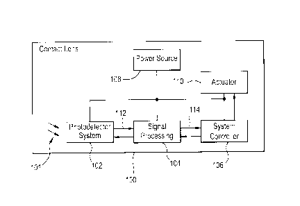
Figure 1 illustrates, in block diagram form, an exemplary powered or
electronic
contact lens 100 comprising a photodetector system 102, a signal processing
circuit
104, a system controller 106, a power source 108 and an actuator 110. When the
contact lens 100 is placed onto the front surface of a user's eye the
photodetector
system 102 may be utilized to detect ambient light, variation in incident
light levels or
infrared communication signals. The functionality and operation of each of the
components comprising the exemplary powered contact lens 100 is described
below.
In this exemplary embodiment, the photodetector system 102 may be embedded
into the contact lens 100, receive ambient or infrared light 101, and provide
to the signal
processing circuit 104 a data signal 112 having a value representative of the
light
energy incident on the contact lens 100. The photodetector system 102 and the
signal
processing circuit 104 may be configured for two-way communication. In other
words,
the signal processing circuit 104 may provide one or more signals to the
photodetector
system 102, examples of which are set forth subsequently. The signal
processing
circuit 104 may be utilized for digital signal processing, including one or
more of filtering,
processing, detecting, and otherwise manipulating/processing data to permit
incident
light detection for downstream use. The signal processing circuit 104 may be
configured
to detect predetermined sequences of light variation indicative of specific
blink patterns
or infrared communication protocols. Upon detection of a predetermined
sequence the
signal processing circuit 104 may provide an indication signal 114 to the
system
controller 106, and in response the system controller 106 may act to change
the state of
actuator 110, for example, by enabling, disabling or changing an operating
parameter
such as an amplitude or duty cycle of the actuator 110. The system controller
106 and
13
CA 02939027 2016-08-16
the signal processing circuit 104 may be configured for two-way communication.
In
other words, the system controller 106 may provide one or more signals to the
signal
processing circuit 104, examples of which are set forth subsequently.
The system controller 106 may provide a feedback signal to the photodetector
system 102 to adjust the gain of the photodetector system 102 in response to
ambient
light levels in order to maximize the dynamic range of the system.
In some embodiments the signal processing circuit 104 may be implemented as
a digital logic circuit and the photodetector system 102 configured to provide
a digital
data signal 112. The system controller 106 also may be implemented as a
digital logic
circuit and implemented as a separate component or integrated with signal
processing
circuit 104. The signal processing circuit 104 and system controller 106 may
be
implemented in custom logic, reprogrammable logic or one or more
microcontrollers as
are well known to those of ordinary skill in the art. The signal processing
circuit 104 and
system controller 106 may comprise associated memory to maintain a history of
values
of the data signal 112 or the state of the system. It is important to note
that any suitable
arrangement and/or configuration may be utilized.
A power source 108 supplies power for numerous components comprising the
contact lens 100. The power may be supplied from a battery, energy harvester,
or other
suitable means as is known to one of ordinary skill in the art. Essentially,
any type of
power source 108 may be utilized to provide reliable power for all other
components of
the system. A blink sequence or an infrared communication signal having a
predetermined sequence or message value may be utilized to change the state of
the
system and/or the system controller as set forth above. Furthermore, the
system
controller 106 may control other aspects of a powered contact lens depending
on input
from the signal processor 104, for example, changing the focus or refractive
power of an
electronically controlled lens through the actuator 110. As illustrated, the
power source
14
CA 02939027 2016-08-16
108 is connected to each of the other components and would be connected to any
additional element or functional block requiring power.
The actuator 110 may comprise any suitable device for implementing a specific
action based upon a received command signal. For example, if a blink
activation
sequence is detected as described above, the system controller 106 may enable
the
actuator 110 to control a variable-optic element of an electronic or powered
lens. The
actuator 110 may comprise an electrical device, a mechanical device, a
magnetic
device, or any combination thereof. The actuator 110 receives a signal from
the system
controller 106 in addition to power from the power source 108 and produces
some
action based on the signal from the system controller 106. For example, if the
system
controller 106 signal is indicative of the wearer trying to focus on a near
object, the
actuator 110 may be utilized to change the refractive power of the electronic
ophthalmic
lens, for example, via a dynamic multi-liquid optic zone. In an alternate
exemplary
embodiment, the system controller 106 may output a signal indicating that a
therapeutic
agent should be delivered to the eye(s). In this exemplary embodiment, the
actuator 110
may comprise a pump and reservoir, for example, a microelectromechanical
system
(MEMS) pump. As set forth above, the powered lens of the present invention may
provide various functionality; accordingly, one or more actuators may be
variously
configured to implement the functionality.
Figure 2 illustrates, in part schematic diagram, part block diagram form, a
photodetector system 200 in accordance with an exemplary embodiment of the
present
invention. The photodetector system 200 comprises a photodiode array 202
including a
plurality of individual photodiodes, an integrate-and-hold circuit 204, and an
analog-to-
digital converter 206 providing an output data signal 208. The photodiode
array 202
comprises one or more photodiodes DG1 to DG5 having cathode terminals
selectively
coupled to a cathode node 210. In other exemplary embodiments, the photodiode
array
202 may comprise additional photodiodes, fewer photodiodes or even a single
photodiode. The selective coupling is determined by a value of a gain signal
pd_gain
CA 02939027 2016-08-16
which may be provided by a signal processing circuit, for example, signal
processing
circuit 104 illustrated in Figure 1. A detailed explanation of the photodiode
construct is
given subsequently. In some embodiments when one of the one or more
photodiodes
DG1 to DG5 is not coupled to cathode node 210, its cathode terminal may be
coupled
to a circuit ground to discharge the parasitic capacitance associated with the
semiconductor diode junction. The one or more photodiodes DG1 to DG5 generate
photocurrent in response to incident light 212. Silicon semiconductor
photodiodes
typically generate photocurrent having a value proportional to incident light
energy and
also generate a "dark current" due to leakage mechanisms and which is present
independent of incident light and may be proportional to temperature and
voltage across
the photodiode. Therefore the total current generated by the photodiode array
202
comprises a component determined by incident light 212 and a dark current
component
generated by the selected one or more photodiodes DG1 to DG5. Silicon
semiconductor
photodiodes further comprise a junction capacitance.
Integrate-and-hold circuit 204 comprises an integration capacitor Cint, a hold
switch S3 and a precharge switch S4. Hold switch S3 selectively couples
cathode node
210 to the integration capacitor Cint based on a value of a hold signal holdB.
Preferably
the hold switch S3 is configured to be closed when the hold signal holdB
presents a
logic one or high voltage value and to be open when the hold signal holdB
presents a
logic zero or low voltage value. Precharge switch S4 selectively couples the
integration
capacitor Cint to a reference voltage vref based on a value of a precharge
signal
PRECHRG. Preferably the precharge switch S4 is configured to be closed when
the
precharge signal PRECHRG presents a logic one or high voltage value and to be
open
when the precharge signal PRECHRG presents a logic zero or low voltage value.
The
integration capacitor Cint is further coupled to an integrated output voltage
node
Int_vout. In operation, integration capacitor Cint is precharged to reference
voltage vref
and then integrates the current drawn by the photodiode array 202 to develop
an
integrated output voltage Int_vout.
16
CA 02939027 2016-08-16
Analog-to-digital converter 206 is configured to receive the voltage developed
on
integration capacitor Cint and provided on integrated output voltage node
Int_vout and to
provide a digital output value Dout representative of the integrated output
voltage. The
analog-to-digital converter 206 may be configured to receive an enable signal
adc_en_rst. In some exemplary embodiments the analog-to-digital converter 206
is
configured to be reset when adc_en_rst presents a logic zero value, and to
commence
a conversion operation when adc_en_rst transitions to a logic one value.
In this exemplary embodiment the gain signal pd_gain is a five-bit digital
signal
notated pd_gain<4:0> allowing the total photocurrent generated by photodiode
array
202 to be appropriately scaled to accommodate the incident light intensity.
Further in
this exemplary embodiment, photodiodes DG1, DG2, DG3, DG4 and DG5 comprises 1,
7, 56, 448 and 3584 photodiode elements, respectively. At very high incident
light
intensity, photocurrent from only one photodiode element cathode (DG1) may be
output
to the integrator with all remaining cathodes shorted to ground. At lower
light intensity,
photodiodes DG1 and DG2 may both be selected providing eight times the
sensitivity of
photodiode DG1. Likewise for progressively lower intensities, selection of
photodiodes
DG1, DG2, and DG3 provides 64 times the sensitivity of photodiode DG1, and
selection
of photodiode groups DG1 through DG4 provides 512 times the sensitivity of
photodiode DG1. At the lowest usable light intensities, selection of
photodiodes DG1
through DG5 provides 4096 times the sensitivity of photodiode by selecting all
4096
photodiode elements in the array. This allows digital control via the gain
signal pd_gain
of the sensitivity of the photodiode array 202 over a 72 dB range.
Figure 3 illustrates a timing diagram of an integration and conversion
sequence
of the exemplary photodetector system 200 illustrated in Figure 2. First, at
the time
indicated by 301, the hold signal holdB is set to a high voltage value closing
the hold
switch S3 and thus coupling the integration capacitor Cint to cathode node 210
and
photodiode array 202. Then at 302 the precharge signal PRECHRG is asserted,
closing
precharge switch S4 and coupling integration capacitor Cint, cathode node 210
and the
17
CA 02939027 2016-08-16
junction capacitance of the selected one or more photodiodes DG1 to DG5 to
reference
voltage vref. It is important to note that while the voltage on the
integration capacitor
Cint, as illustrated in the trace labeled Int_vout, is shown as a constant
value prior to
time 302, the voltage may be any reasonable value as determined by the
incident light
on the photodetector system (Figure 2), time elapsed since prior actions and
other
similar functions as is understood by those of ordinary skill in the art. Next
at 303 the
precharge signal PRECHRG is de-asserted, disconnecting the reference voltage
vref
and allowing the current drawn by the photodiode array 202 to discharge
integration
capacitor Cint. After an integration time Tint, the hold signal holdB is set
to a low voltage
value at 304, opening the hold switch S3. Then at 305 the enable signal
adc_en_rst is
driven to a logic zero value and subsequently to a logic one value to start a
conversion
operation. After a conversion time Tadc the digital output value Dout presents
a new
value representative of integrated voltage Vint. In this exemplary embodiment
the
integration voltage is represented by the difference between the reference
voltage vref
and the voltage on the integration capacitor Cint provided on integrated
output voltage
node Int_vout.
Each of the one or more photodiodes DG1 to DG5 may be modeled as a current
source. The total current generated by the photodiode array 202 may be
integrated with
the integration capacitor Cint. No op-amps are required in the signal chain
which in turn
allows for very low power dissipation. At the end of the integration time
Tint, the resulting
voltage at the integrator output is given by
Int_vout=vref-(IPDICtnt)'Tint, (1)
where Tint is the integration period and IPD is total current generated by the
photodiode
array 202. As seen from this equation, an equivalent resistance, Rgain, which
determines the trans-resistance gain, and that transforms the input current to
the output
voltage, is given by
18
CA 02939027 2016-08-16
Rgain=TtntlCint. (2)
As may be seen from equation 2, Rgain is directly proportional to Tint and
inversely proportional to C. For purposes of this discussion, this may be
thought of as
being a time-varying resistor. So, for example, to increase the gain, we can
increase the
integration interval Tint, and /or reduce the integration capacitor Cint. A
higher gain value
may therefore be achieved with a smaller capacitor and hence translates to a
smaller
die size, once again, a preferable design parameter. To adjust the gain, one
could
therefore switch in or out additional capacitance and/or change the
integration time Tint,
for example, via digital control.
Note that extremely large values for Rgain may be achieved with very small
area,
and thus the circuit of the present invention is suitable for integration in a
semiconductor
die and for use in a biomedical device such as a powered contact lens. For
example,
with Cint = 1pF and Tint = 100mS, Rgain = 100GQ, which may be achieved in an
area of
only approximately 14pm x 14,um in a typical 0.18 pm complementary metal-oxide
semiconductor (CMOS) process.
The voltage provided on integrated output voltage node Int_vout (equation 1),
is
then digitized by the analog-to-digital converter 206. A full-scale output of
the analog-to-
digital converter corresponds to Vint = vref and to a voltage of OV on
integrated output
voltage node Int_vout, and corresponds to a full-scale photo-current IPD(FS)
given by
(FS)=Cint=vref /Tint. (3)
A periodically time-varying impulse response corresponding to the integration
and hold operation may be described by the time varying impulse response
h(t,t),
wherein
h(r,t)=u(-0-24/-+(N-1 )-T (4)
19
CA 02939027 2016-08-16
over interval (N-1).Tint< t 0=Tint), N=1,2,3,....
Equation 4 gives the impulse response h(r,t) at time t, where N is an integer
representing a given integration time interval. Equation 4 shows that the time-
varying
impulse response is a pulse whose width increases linearly with t up to
t=Tint. Then, at
t=Tint+, the impulse-response pulse width drops back to zero width (it is
reset), and
begins to increase again until t=2Tint (it is periodic, with period = Tint).
The plus sign,
in t=Tint+ is meant to indicate that the calculation starts at the instant
after t=Tint=
At the end of each integration interval, we have t=N*Tint (N =1,2,3,...), and
from
equation 4, the impulse response is given by
h(r,N=T1nt)=u(r)-u(-1--Tint). (5)
The Laplace transform transfer function of the impulse response at the end of
each integration interval (equation 5) is given by
H(s)= [1-e-(s= Tint)] I (s=T int). (6)
Letting s = j2rif in equation 6, and then simplifying, results in the Fourier
transform of the integration and hold operation which is given by
H(j2n-f)= e-cgTint.f)sin(g=T f)/(g=T int' f). (7)
As may be seen from equation 7, the resultant frequency response magnitude is
inversely proportional to the frequency, f (which provides 20dB/dec roll-off),
and is
punctuated by periodic zeros (notches).
CA 02939027 2016-08-16
Figure 4 illustrates the frequency response magnitude versus frequency for an
integration time Tint of 0.1s and having periodic zeros (notches) at multiples
of 10Hz. It
will be appreciated that the normalized frequency response of equation 7 is
independent
of Cint. That is, the corner frequency and shape of the frequency response is
independent of Cint, and depends only on the length of the integration
interval, Tint.
As may be seen in equation, the frequency response phase is perfectly linear
with a delay of given by
Tde1ay=Tint/2. (8)
The periodic notches occur at frequencies, fN, which is given by
fN=All 7' Ent, (9)
where N=1, 2, 3....
Choosing the ADC sampling frequency as
fs=11 int. (10)
The frequency response illustrated in Figure 4 with Tint = 0.1s (fs=10Hz), has
a
3dB corner frequency of 4.4Hz, transitioning to a first notch (infinite
attenuation) at
10Hz. The integration and hold operation therefore serves as a very effective
anti-alias
filter, attenuating frequencies very rapidly above the Nyquist frequency
(fs/2). No
additional anti-alias filter circuits are required for many ambient light or
infrared
communication applications, thus minimizing the required area for the
photodetector
system of the present invention.
21
CA 02939027 2016-08-16
The periodic notches also extend to multiples of AC line frequencies (50Hz or
60Hz). This has the added benefit of additional fluorescent light flicker
rejection beyond
the already approximately 30dB of rejection at 100Hz or 120Hz resulting from
the
20dB/dec roll off above the 4.4Hz corner. Another choice for T=1/Fs is 83.33..
.ms
providing notches at multiples of 12Hz and a -3dB corner frequency of 5.33Hz.
The total current required for the integrate-and-reset function is given by
the
current required to pre-charge Cint to vref every sampling period or cycle.
The average
current assuming the integration capacitor Cint is fully discharged each cycle
is given by
lavg=vref= C inta int. (11)
By way of illustration, for a photodetector system having vref = 1.8V, Cint =
145pF, and T1nt=100mS the average current lavg = 2.6nA (nominal) for the
integrator.
This assumes that Cint is fully discharged by the photodiode current every
sampling
period or cycle. It will be appreciated that the average supply current is
equal to the
average total current generated by the photodiode array 202.
Lower power dissipation therefore requires lower current generated by the
photodiode array 202 and a smaller value of the integration capacitor Cint for
a full-scale
transition over the integration time Tint. Overall, the optimal lowest power,
smallest
design may have a photodiode array 202 comprising minimum-size photodiode
junctions and a small integration capacitor Cint. As will be appreciated by
those skilled in
the art, the smallest sizes may be limited by sampling noise, switch charge
injection and
other considerations related to circuit and device non-idealities.
Figure 5 illustrates, in part schematic diagram, part block diagram form, a
photodetector system 500 having dark current cancellation in accordance with
another
exemplary embodiment of the present invention. The photodetector system 500
comprises a photodiode array 502 comprising photodiodes DG1 to DG5 coupled to
a
first cathode node 504, a first integrate-and-hold circuit 506, a dark
photodiode array
22
CA 02939027 2016-08-16
508 coupled to a second cathode node 510, a second integrate-and-hold circuit
512, an
input select switch 514, an analog-to-digital converter 516, a first register
518, a second
register 520 and a subtractor 522 providing an output data signal 524. The
photodiode
array 502 and the integrate-and-hold circuit 506 operate to develop a first
integrated
voltage Int_vout in a similar manner to the photodiode array 202 and the
integrate-and-
hold circuit 204, respectively, of the photodetector system 200 described
above with
respect to Figure 2.
As set forth above, silicon semiconductor photodiodes generate a dark current
due to leakage mechanisms and which is present independent of incident light
and may
be proportional to temperature and voltage across the photodiodes.
Accordingly, a dark
current photodiode array be utilized to compensate as described in detail
subsequently.
The dark current photodiode array 508 comprises one or more photodiodes DG1a
to
DG5a having cathode terminals selectively coupled to a cathode node 510. In a
manner
similar to the photodiode arrays 202 and 502, the selective coupling in the
dark current
photodiode array 508 is determined by a value of a pd_gain signal which may be
provided by a signal processing circuit. In some exemplary embodiments when
one of
the one or more photodiodes DG1a to DG5a is not coupled to second cathode node
510, its cathode terminal may be coupled to a circuit ground to discharge the
parasitic
capacitance associated with the semiconductor diode junction. The one or more
photodiodes DG1a to DG5a are covered with a light blocking layer, such as a
metal
layer, so that they do not generate photocurrent in response to incident light
526.
However, any suitable light blocking layer or coating may be utilized.
Therefore the total
current generated by the dark photodiode array 508 comprises only a dark or
leakage
current component generated by the selected one or more photodiodes DG1a to
DG5a.
It will be appreciated by those skilled in the art that if the photodiodes
DG1a to DG5a
and DG1 to DG5 are manufactured together, for example, in the same silicon
wafer,
and if the corresponding photodiodes (DG1 and DG1a, DG2 and DG2a, etc.) have
the
same active dimensions and area, that the dark currents generated by
photodiodes
23
CA 02939027 2016-08-16
DG1a to DG5a are very similar in magnitude to dark currents generated by
photodiodes
DG1 to DG5 of photodiode array 502.
The second integrate-and-hold circuit 512 comprises a second integration
capacitor Cinta, a second hold switch S3a and a second precharge switch S4a.
Second
hold switch S3a selectively couples second cathode node 510 to the second
integration
capacitor Cinta based on a value of a hold signal holdB. Preferably the second
hold
switch 53a is configured to be closed when the hold signal holdB presents a
logic one
or high voltage value to be open when the hold signal holdB presents a logic
zero or low
voltage value. Second precharge switch S4s selectively couples the second
integration
capacitor Cinta to a reference voltage vref based on a value of a precharge
signal
PRECHRG. Preferably the second precharge switch S4a is configured to be closed
when the precharge signal PRECHRG presents a logic one or high voltage value
to be
open when the precharge signal PRECHRG presents a logic zero or low voltage
value.
The second integration capacitor Cinta is further coupled to an integrated
output voltage
node Int_vout. In operation, the second integration capacitor Cinta is
precharged to
reference voltage vref and then integrates the current drawn by the dark
photodiode
array 506 to develop a second integrated output voltage Int_vouta.
Input select switch 514 is configured to selectively couple one of either the
first
integrated output voltage Int_vout or the second integrated output voltage
Int_vouta to
an input of the analog-to-digital converter 516. The selective coupling may be
determined based on a select control signal sel provided by a signal
processing circuit
or controller.
Analog-to-digital converter 516 is configured to receive the voltage
selectively
coupled by input select switch 514 and to provide a digital output value. In
this
exemplary embodiment the analog-to-digital converter 516 selectively stores
the digital
output value corresponding to integrated output voltage Int_vout in first
register 518 and
the digital output value corresponding to integrated output voltage Int_vouta
in second
24
CA 02939027 2016-08-16
register 520. The selective storing may be determined based on the select
control signal
sel. The analog-to-digital converter 516 may be configured to receive an
enable signal
adc_en_rst. In some exemplary embodiments the analog-to-digital converter 516
is
configured to be reset when adc_en_rst presents a logic zero value and to
commence a
conversion operation when adc_en_rst transitions to a logic one value. The
subtractor
522 generates output data signal 524 based on a difference between the values
held in
first register 518 and second register 520. In this manner the output data
signal 514
represents the integrated photocurrent from photodiode array 502 and the
difference in
dark currents between photodiode array 502 and the dark photodiode array 508.
If the
dark currents are very similar in magnitude and if the integration times are
the same
then the difference in dark currents will be nearly zero, and thus the output
data signal
514 will represent the integrated photocurrent from photodiode array 502.
In a manner similar to that described for the photodetector system 200, at
very
low light intensity, all 4096 photodiodes in the photodiode arrays 502 and 508
may be
selected via a 5-bit gain control pd_gain<4:0>. This provides the maximum
junction area
for photocurrent generation providing the highest photo sensitivity, but also
generates
the highest dark current. For improved signal to noise ratio (SNR), or
photocurrent to
dark current ratio, the photodetector system 500 measures and mathematically
cancels
the unwanted dark current component, to the extent that the photodiode array
502 and
the dark photodiode array 508 and the first integration and hold circuit 506
and the
second integration and hold circuit 512, respectively, match.
Figure 6 illustrates exemplary light-blocking and light-passing features on an
integrated circuit die 600. The integrated circuit die 600 comprises a light-
passing region
602, a light-blocking region 604, bond pads 606, passivation openings 608, and
light-
blocking layer openings 610. The light-passing region 602 is located above the
photodiode array or arrays (not illustrated), for example, an array of
photodiodes
implemented in the semiconductor process. In a preferred exemplary embodiment,
the
light-passing region 602 permits as much light as possible to reach the
photodiodes
CA 02939027 2016-08-16
thereby maximizing sensitivity. This may be done through removing polysilicon,
metal,
oxide, nitride, polyimide, and other layers above the photodiode array or
arrays, as
permitted in the semiconductor process utilized for fabrication or in post
processing. The
light-passing area 602 may also receive other special processing to optimize
light
detection, for example an anti-reflective coating, filter, and/or diffuser.
The light-blocking
region 604 may cover other circuitry on the die which does not require light
exposure.
The performance of the other circuitry may be degraded by photocurrents, for
example,
shifting bias voltages and oscillator frequencies in the ultra-low current
circuits required
for incorporation into contact lenses, as mentioned previously. The light-
blocking region
604 is preferentially formed with a thin, opaque material, for example,
aluminum,
copper, or titanium already use in semiconductor wafer processing and post
processing.
If implemented with electrically conductive metal, the material forming the
light-blocking
region 604 must be insulated from the circuits underneath and the bond pads
606 to
prevent short-circuit conditions. Such insulation may be provided by the
passivation
already present on the die as part of normal wafer passivation, e.g. oxide,
nitride, and/or
polyimide, or with other dielectric added during post-processing. Masking
permits light
blocking layer openings 610 so that conductive light-blocking metal does not
overlap
bond pads on the die. The light-blocking region 604 is covered with additional
dielectric
or passivation to protect the die and avoid short-circuits during die
attachment. This final
passivation has passivation openings 608 to permit connection to the bond pads
606.
Figure 7 illustrates an exemplary contact lens with an electronic insert
comprising
a blink detection system in accordance with the present invention. The contact
lens 700
comprises a soft plastic portion 702 which comprises an electronic insert 704.
This
insert 704 includes a lens 706 which is activated by the electronics, for
example,
focusing near or far depending on activation. Integrated circuit 708 mounts
onto the
insert 704 and connects to batteries 710, lens 706, and other components as
necessary
for the system. The integrated circuit 708 includes a photodiode array 712 and
associated photodetector signal path circuits. The photodiode array 712 faces
outward
through the lens insert and away from the eye, and is thus able to receive
ambient light.
26
CA 02939027 2016-08-16
The photodiode array 712 may be implemented on the integrated circuit 708 (as
shown)
for example as a single photodiode or array of photodiodes. The photodiode
array 712
may also be implemented as a separate device mounted on the insert 704 and
connected with wiring traces 714. When the eyelid closes, the lens insert 704
including
photodetector 712 is covered, thereby reducing the light level incident on the
photodetector 712. The photodetector 712 is able to measure the ambient light
and/or
infrared light.
Additional considerations of the photodetector system of the present invention
allow for further reduction in the required area, volume or cost of the
photodetector
system and powered or electronic ophthalmic lenses into which the system may
be
incorporated.
The integration capacitances Chit may be formed partly by an input capacitance
of the analog-to-digital converter, such as a feedback DAC capacitor array in
a
successive approximation analog-to-digital converter (SAR ADC). Note that this
would
apply in the case of the exemplary embodiments described with Figure 5 if the
integration periods for the two photodiode arrays are not simultaneous.
In the photodetector system of Figure 5, a single analog-to-digital converter
is
used for conversion of two quantities. An alternative embodiment may employ
two
analog-to-digital converters, but using one provides for cancellation of any
offset
inherent in the analog-to-digital converter itself whereas a system with two
analog-to-
digital converters would have a residual offset corresponding to the mismatch
in offsets
between the converters.
Preferably the photodiode arrays are implemented in a CMOS technology to
increase integration ability and reduce the overall size of the photodetector
system and
the signal processing and system controller circuitry. Preferably the
photodetector
system, the signal processing circuitry and the system controller circuitry
are integrated
27
CA 02939027 2016-08-16
together in a single silicon die, reducing area required in the powered or
electronic
ophthalmic lens for interconnection traces and on the die for bonding or
bumping pads.
It will be appreciated by those skilled in the art that the photodiode array
may
comprise fewer photodiodes when lower dynamic range is required. For example,
in
some embodiments a photodiode array comprising a single photodiode may be
sufficient. The photodiodes may comprise a single photodiode element. However
the
best gain scaling may be achieved by implementing the larger photodiodes with
a
number of interconnected (e.g. in parallel) photodiode elements of a common
design
(dimensions, area, diffusion types).
Although shown and described in what is believed to be the most practical and
preferred embodiments, it is apparent that departures from specific designs
and
methods described and shown will suggest themselves to those skilled in the
art and
may be used without departing from the spirit and scope of the invention. The
present
invention is not restricted to the particular constructions described and
illustrated, but
should be constructed to cohere with all modifications that may fall within
the scope of
the appended claims.
28