Note: Descriptions are shown in the official language in which they were submitted.
I
CA 02939202 2016-08-09
, 56304-1
High Performance Standard Cell
CROSS-REFERENCE TO RELATED APPLICATIONS
[0001] This application claims priority to the filing date of U.S. Patent
Application
Serial No. 14/195,525, filed March 3, 2014.
TECHNICAL FIELD
[0002] This application relates to processors, and more particularly, to power
optimization for processors.
BACKGROUND
[0003] As semiconductor technology advances into the deep sub-micron process
nodes, short channel effects can severely degrade performance. The carrier
velocity saturates
in such short channels, which slows switching speeds and reduces transistor
strength. To
achieve high density yet have adequate transistor strength, strain engineering
techniques have
been developed so that the crystal lattice is strained in the source and drain
diffusion regions
(these diffusion regions are typically denoted as oxide definition (OD) with
regard to
transistor layout terminology). The OD is not only doped n-type or p-type as
appropriate to
achieve the desired transistor type (NMOS or PMOS), but is also strained to
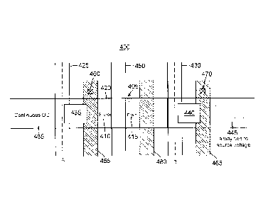
increase carrier
velocity and transistor strength. In that regard, the OD is just locally
strained as opposed to
straining the entire substrate.
1
CA 02939202 2016-08-09
WO 2015/134202 PCT/US2015/016690
[0004] Such local strain has proven to be superior to a global strain across
the
entire substrate. The type of strain depends upon the transistor type. The OD
for
PMOS transistors is compressively strained whereas the OD for NMOS transistors
has
tensile strain. For example, a film of SiGe may be applied to p-type OD to
introduce
compressive strain whereas a film of SiN or SiC may be applied to n-type OD to
introduce tensile strain. The resulting strain engineering of silicon has
proven to be
quite successful for the achievement of satisfactory transistor strength in
deep sub-
micron process nodes.
[0005] The use of strain engineering introduces a number of constraints into
the
layout process. Figure 1 illustrates the layout for an example pair of
transistors. A first
transistor 100 has its source (S) and drain (D) defined by a first OD region
105. A
polysilicon gate 110 separates the source and drain regions. A similar
arrangement of
another OD region 115 and polysilicon gate 120 defines another transistor 101.
At
advanced process nodes, the layout of Figure 1 would be inefficient because OD
115
and 110 forming the drain and source regions are both relatively short. Such a
short
length to the OD allows its crystal lattice to relax too much despite the use
of local
strain engineering. Transistors 100 and 101 would thus be too weak. In
contrast, if
ODs 105 and 115 could be extended to form a continuous OD as shown by the
dotted
lines 125, ODs 105 and 115 could have increased strain, resulting in better
performance.
But such an extension of the ODs would short the drain of transistor 100 to
the source
of transistor 101.
[0006] To achieve satisfactory transistor performance in the deep sub-micron
process nodes, "continuous OD" layouts have been developed. Figure 2
illustrates an
example layout for a continuous OD 200. Transistors 100 and 101 are still
defined with
respect to polysilicon gates 110 and 120, respectively. But OD 200 is
continuous for
2
CA 02939202 2016-08-09
WO 2015/134202
PCT/US2015/016690
both transistors such that it can develop adequate lattice strain for
satisfactory transistor
strength. A dummy polysilicon gate 205 electrically isolates transistors 100
and 101 by
being configured to be charged to the source voltage. For example, if OD 200
is doped
p-type, dummy gate 205 would be tied to the power supply voltage VDD.
Alternatively, if OD 200 is doped n-type, dummy gate 205 would be tied to
ground. A
similar dummy gate 210 isolates transistor 100 from a transistor (not
illustrated) to the
left of dummy gate 210 in continuous OD 200.
[0007] Although the use of continuous OD 200 enables sufficient crystal
lattice
strain to be achieved, there are a number of design complications. For
example, each
transistor may be considered to reside within a separate "standard cell." A
standard cell
201 that forms transistor 100 extends from a border A along dummy gate 210 to
a
border B along dummy gate 205. Each dummy gate is always tied to a source
voltage ¨
in a PMOS embodiment, the source voltage is VDD whereas it is ground in an
NMOS
embodiment. An interconnect 215 provides the source voltage coupling between
dummy gate 205 and the source of transistor 101. Similarly, an interconnect
220
provides the source voltage coupling between dummy date 210 and the source of
transistor 100. With this standard cell topology in mind, note the problems
that arise
with regard to characterizing the leakage for standard cell 201. With regard
to the
leakage from the drain for transistor 100, it can only be defined at the cell
level with
regard to the leakage across gate 110 from the source for transistor 100. But
this
leakage current from the source for transistor 100 in turn depends upon the
state for
diffusion region 225 to the left of dummy gate 210. A priori, before standard
cell 201 is
instantiated next to another standard cell, it cannot be known whether
diffusion region
225 is the source or the drain for another transistor in this additional
standard cell. This
uncertainty greatly complicates the leakage calculation for transistor 100.
For example,
3
CA 02939202 2016-08-09
WO 2015/134202
PCT/US2015/016690
suppose diffusion region 225 forms another transistor source ¨ it will then be
at the
same voltage as the source for transistor 100 such that no leakage can occur
across
dummy gate 210. Conversely, if diffusion region 225 forms another transistor
drain,
then a leakage current will flow from the source for transistor 101 to
diffusion region
225. We know that a leakage current will always be present across gate 110
between
the drain and source for transistor 100. This leakage current may be denoted
as the
"always-present" leakage current to distinguish it from the "optional" leakage
current
that depends upon whether diffusion region 225 forms a drain or a source. So
there
exists two possibilities for a standard cell such as cell 201: just the always-
present
leakage current or a sum of the always-present leakage current and the
optional leakage
current. The leakage current characterization is a very important performance
hallmark
of a design. But the conventional standard cell architecture shown in Figure 2
for
continuous OD 200 greatly complicates the leakage current determination for a
given
design.
[0008] Accordingly, there is a need in the art for improved standard cell
continuous OD architectures
SUMMARY
[0009] A cell architecture is disclosed which provides a consistent leakage
current characterization for continuous oxide definition (OD) region
processes. In that
regard, a "cell" refers to the layout for a circuit building block such as a
logic gate or an
inverter. Such a circuit building block typically comprises several
transistors but
embodiments disclosed herein may also include just one transistor. A
conventional cell
may be deemed to extend from a first dummy gate across to a second dummy gate.
Within the dummy gate boundaries, there may be one or more gates, depending
upon
4
CA 02939202 2016-08-09
WO 2015/134202
PCT/US2015/016690
the number of transistors. Similarly, one or more continuous OD regions may
extend
across the cell. These continuous OD regions may also be denoted as continuous
active
regions. For example, if a cell is to contain both NMOS and PMOS transistors,
it would
need at least two continuous OD regions ¨ at least one doped p-type active
region for
the PMOS transistors and at least one doped n-type active region for the NMOS
transistors. In a conventional cell, the cell structures would stop at the
dummy gate
boundaries. But the advantageous cell disclosed herein demands an extension
beyond
the dummy gate adjacent the transistor's drain. In that regard, the transistor
has a drain
and a source each defined in the OD region so as to be separated by the
transistor's gate.
The drain is thus defined in a portion of the OD region that stretches from
the gate to a
first side of the adjacent dummy gate. This adjacent dummy gate to the drain
may also
be denoted herein as the drain-side dummy gate. The remaining dummy gate may
thus
be denoted as the source-side dummy gate.
[0010] The drain-side dummy gate includes an opposing second side. In a
conventional cell, there is no structure that carries over to a portion of the
OD region
adjacent this opposing second side of the drain-side dummy gate. But as will
be
explained further below, the cell discussed herein includes a local
interconnect structure
that couples the drain-side dummy gate and the portion of the OD region
adjacent the
opposing second side of the drain-side dummy gate to a source voltage. This is
quite
advantageous because the drain for the cell is guaranteed to always be
separated by the
drain-side dummy gate from a portion of the OD region charged to the source
voltage.
Note that the OD region including the cell will typically including numerous
other cells.
These cells may be deemed to extend from a first cell to a last cell. But even
if the cell
is the last cell (or the first cell) such that there would be no further cells
defined in the
portion of the OD region adjacent the second side of the drain-side dummy
gate, this
CA 02939202 2016-08-09
56304-1
portion of the OD region will act no differently from a transistor source with
regard to the
leakage current that flows from this portion of the region across the drain-
side dummy gate to
the drain. In other words, there may be a cell defined in this portion of the
OD region or there
may not be. Regardless of whether there is another cell adjacent the drain-
side dummy gate,
the portion of the OD region adjacent the second side of the drain-side dummy
gate is charged
to the source voltage.
[0011] Given this cell architecture, the uncertainty discussed above with
regard to
conventional continuous OD cell leakage has been alleviated. The resulting
cell always
provides a consistent, predictable leakage. In that regard, note that the cell
requires no local
interconnect extension beyond the source-side dummy gate to the continuous OD
region
outside of the source-side dummy gate. It may be that an additional cell is
defined in this
portion continuous OD region to have a drain. It is true that leakage current
will flow from
the source of the present cell to the drain of this additional cell. But such
an additional
leakage current does not upset the leakage current characterization at the
cell level because
this additional cell has the same structure and thus measures this leakage
current as its own.
Conversely, if this neighboring cell abuts with its source, there is no
leakage current between
the neighboring cells due to the source-to-source abutment.
[0011a] According to one aspect of the present invention, there is provided a
cell
comprising: a continuous oxide definition (OD) region defined in a substrate;
a gate for a
transistor between a first dummy gate and a second dummy gate, wherein a
source for the
transistor is defined in a first portion of the continuous OD region between
the gate and the
first dummy gate, and wherein a drain for the transistor is defined in a
second portion of the
continuous OD region between the gate and a first side of the second dummy
gate; a first gate-
directed local interconnect coupled to a third portion of the continuous OD
region adjacent a
second opposing side of the second dummy gate; a first diffusion-directed
local interconnect
configured to couple the first gate-directed local interconnect to the second
dummy gate; and
a first via configured to couple the first diffusion-directed local
interconnect to a source
voltage interconnect in a metal layer adjacent the substrate.
6
CA 02939202 2016-08-09
56304-1
[0011b] According to another aspect of the present invention, there is
provided a
method for forming a cell, comprising: forming a continuous oxide definition
(OD) region
defined in a substrate; forming a gate for a transistor arranged according to
a gate pitch
between a first dummy gate and a second dummy gate, wherein a source for the
transistor is
defined in a portion of the continuous OD region between the gate and the
first dummy gate,
and wherein a drain for the transistor is defined in a portion of the
continuous OD region
between the gate and a first side of the second dummy gate; forming a first
gate-directed local
interconnect coupled to a portion of the continuous OD region adjacent a
second opposing
side of the second dummy gate; forming a first diffusion-directed local
interconnect
configured to couple the first gate-directed local interconnect to the second
dummy gate; and
forming a via configured to couple the first gate-directed local interconnect
to a source
voltage supply.
BRIEF DESCRIPTION OF THE DRAWINGS
[0012] Figure 1 illustrates a conventional pair of transistor having non-
continuous
diffusion regions.
[0013] Figure 2 illustrates a conventional pair of transistors in a continuous
diffusion
region.
[0014] Figure 3 is a cross-sectional view of multi-level local interconnects
and
6a
CA 02939202 2016-08-09
WO 2015/134202 PCT/US2015/016690
associated structures.
[0015] Figure 4A illustrates a layout for a cell in a continuous diffusion
region,
wherein a transistor includes a drain adjacent a first side of a dummy gate,
and wherein
the cell includes a local interconnect structure configured to charge a
portion of the
diffusion region and the dummy gate to a source voltage.
[0016] Figure 4B illustrates a cell having a mirror-image relationship to the
cell
of Figure 4B.
[0017] Figure 5A illustrates a variation of the cell architecture of Figure 4A
in
which an additional dummy gate is floating.
[0018] Figure 5B illustrates the cell of Figure 5A abutting a drain of a
transistor
in a neighboring cell.
[0019] Figure 6 is a flowchart for an example leakage current analysis of
cells in
accordance with the disclosure.
[0020] Figure 7 is a flowchart for an example method of manufacture for the
cells of Figures 4A through 5B.
DETAILED DESCRIPTION
[0021] To meet the need in for continuous OD standard cells with predictable
leakage currents, a variety of continuous OD standard cell architectures are
disclosed
that provide a known amount of leakage current. In other words, the
uncertainty
discussed above with regard to the conventional layout shown in Figure 2 is
eliminated.
This is remarkably advantageous as one can then confidently predict the
leakage current
just from the number of standard cells that a design incorporates. In
contrast, the
leakage current from a circuit constructed using conventional standard cell
201 of
Figure 2 must be determined through simulation as it will depend on the
various drain-
7
CA 02939202 2016-08-09
WO 2015/134202 PCT/US2015/016690
source or source-to-source cell abutments. In sharp contrast, the leakage
current
calculation for the disclosed cell does not vary regardless of whether it has
a source-to-
source or source-to-drain abutment with a neighboring cell. These advantageous
features may be better appreciated with a discussion of modern local
interconnects.
[0022] Referring again to Figure 2, note that local interconnects 220 and 215
are
shown in simplified form. In reality, a variety of local interconnect layouts
or structures
are known for coupling between gate and non-gate regions. These structures are
disclosed herein with regard to a two-layer local interconnect topology (with
a third
layer dedicated to vias). Although leads in the metal layers adjacent the
substrate are
also sometimes denoted as "local interconnects," such leads are excluded from
the
definition of "local interconnect" as used herein. In older process nodes,
interconnects
in the first metal layer (and higher metal layers) would couple to the
transistor gates and
drain/source terminals through vias. But as semiconductor processing
technology
advanced into the deep sub-micron region, the vias from the first metal layer
(or higher
layers) couple to these transistor structures through a two-layer local
interconnect
structure. The vias are thus in an upper third layer (level 3) between the two
lower
layers of local interconnect (levels 1 and 2).
[0023] Some example two-level local interconnects are shown in Figure 3. As
can be seen in this figure, there are three levels of local interconnects,
ranging from
level Ito level 3. Level 1 defines a layer of local interconnects adjacent a
continuous
diffusion region (OD) 305. Level 3 defines a layer of local interconnects
adjacent a first
metal layer MI. Finally, level 2 defines a layer of local interconnects that
couple
between the level I and level 3 local interconnects.
[0024] A level 1 local interconnect 310 comprises a local interconnect (LI)
type
denoted as LIc. There are two types of local interconnect in level 2: LIa 315
and LIb
8
CA 02939202 2016-08-09
WO 2015/134202
PCT/US2015/016690
320. There is thus one type (LIc 310) in level 1 whereas there are two types
(LIa 315
and Lib 320) in level 2. A level 1 interconnect such as LIc 310 directly
couples to
continuous diffusion region 305. Such a level 1 interconnect would thus be
applied
through an appropriate semiconductor processing mask to continuous diffusion
region
(OD) 305 prior to the formation of any level 2 interconnects. Level 1 is also
the level
for a gate layer 300 such as a polysilicon layer or a high-K metal layer. Gate
layer 300
is not a form of local interconnect as it forms a gate for a transistor having
a source,
drain, and channel in continuous diffusion region 305. Level 2 interconnects
such as
LIa 315 and LIb 320 couple to first metal layer MI (or higher metal layers)
through vias
such as a via VO 325. The vias are arranged in level 3 between level 2 and the
first
metal layer Ml.
[0025] Referring back to Figure 2, the footprints for gate layers 110, 120,
and
205 faun relatively narrow polygons having a longitudinal axis that is
orthogonal to a
longitudinal axis for the polygonal footprint for continuous diffusion region
200. The
local interconnects follow such an organization: a given type of local
interconnect will
generally be arranged so to have a polygonal shape having a longitudinal axis
that is
parallel to either the gate layer or the continuous diffusion region (i.e., to
have a
polygonal footprint with a longitudinal axis that is parallel to a
longitudinal axis for the
polygonal footprint for either the gate layer or the continuous diffusion
region). Since it
is cumbersome to repeatedly refer to the longitudinal axis of a polygonal
shape used for
layout purposes, a local interconnect is defined herein to be a "gate-directed
local
interconnect" if its polygonal footprint has a longitudinal axis parallel to
the
longitudinal axes for the polygonal footprints of the gate layers. Conversely,
a local
interconnect is defined herein to be a "diffusion-directed local interconnect"
if its
polygonal footprint has a longitudinal axis that is parallel to the
longitudinal axes of the
9
CA 02939202 2016-08-09
= 56304-1
polygonal footprints of the diffusion regions.
[0026] A level 1 local interconnect such as LIc 310 is formed on diffusion
region 305.
LIc 310 thus acts as the direct electrical coupling to diffusion region 305
with regard to higher
layers of interconnects. One can thus immediately appreciate that a level 1
local interconnect
must be a gate-directed local interconnect as otherwise it would interfere
with the layout for
the gate layer 300: LIc 310 cannot be a diffusion-directed local interconnect
or it could short
to and intersect gate layer 300. In contrast, level 2 local interconnects can
be either gate-
directed local interconnects or diffusion-directed local interconnects. One
level 2 type of
local interconnect is necessary for coupling to LIc 310 such as LIa 315. Thus,
LIa 315 is a
gate-directed local interconnect and couples between a corresponding via (not
illustrated) in
level 3 to M1 (or higher metal layers). Level 2 LIb 320 couples to gate layer
300 and is
arranged to either have a square footprint (deemed herein to be diffusion-
directed) or to have a
polygonal footprint that is diffusion-directed. LIb 320 may also be denoted
herein as "MP"
320. A via VU coupling between LIb 320 and metal layer M1 is representative of
the level 3
interconnects between M1 and the level 1 and level 2 local interconnects.
First metal layer
M1 lies above level 3. LIa 315, LIb 320, and LIc 310 typically comprise
tungsten whereas via
VU and M1 typically comprises copper. Other materials may be used as known in
the local
interconnect arts.
[0027] With these local interconnect concepts in mind, an example standard
cell 400 is
shown in Figure 4A. Note that this figure (as is the case for all the other
layout figures in this
matter) is a plan view. In other words, whereas Figure 3 was a cross-sectional
view of a
substrate that included OD 305, Figure 4A is showing a plan view of the
substrate's active
surface that supports standard cell 400. In this layout, standard cell 400
includes a transistor
405 having a source 410 and a drain 415 formed in a continuous OD 420. Since
OD 420 is
continuous, standard cell 400 extends from a first dummy polysilicon gate 425
across a
polysilicon gate 450 for transistor 405 to a second dummy gate 430. Note that
cell 400 may
include additional polysilicon gates such as gate 450 for other transistors.
For illustration
clarity, cell 400 is thus shown including just one polysilicon gate 450 but it
will be
appreciated that additional such polysilicon gates may be included in
alternative
CA 02939202 2016-08-09
56304-1
embodiments. Similarly, cell 400 may include additional continuous OD regions
besides
continuous OD 420. A level 2 MP interconnect 435 couples from first dummy gate
425
through a level 1 LIc interconnect 455 to source 410. A via 460 couples
between a metal
layer such as the M1 metal layer (not illustrated) to level 1 LIc interconnect
455 through a
level 2 interconnect LIa layer (not illustrated) so that source region 410 and
dummy gate 425
are charged to the appropriate source voltage (VDD or ground, depending upon
whether
transistor 405 is a PMOS or NMOS transistor, respectively).
[0028] In an analogous fashion to interconnect 435, a level 2 MP interconnect
440
couples from second dummy gate 430 through a level 1 LIc interconnect 465 to a
diffusion
region 445 in OD 420 to the right of dummy gate 430. Since dummy gate 430
should be tied
to a source voltage for it to function as a dummy gate, a via 470 couples
between a source
interconnect in a metal layer (not illustrated) to level 1 LIc interconnect
465 through a level 2
LIa interconnect (not illustrated). Diffusion region 445 is thus also charged
to the source
voltage. As discussed previously, both LIc 465 and the LIa interconnect are
gate-directed
interconnects. In a level 1/level 2 stack of these gate-directed
interconnects, the combination
of the LIa and LIc interconnects may be designated as an MO OD layer. For
example, an
MO-OD layer 480 couples to drain 415.
[0029] Note that cell 400 includes MP interconnect 440, LIc interconnect 465,
11
CA 02939202 2016-08-09
WO 2015/134202
PCT/US2015/016690
and via 470 even though these structures exist outside a traditional cell
boundary, which
would conventionally extend from dotted line A on dummy gate 425 to dotted
line B on
dummy gate 430. These extra structures are quite advantageous because they
force
diffusion region 445 to always be charged to the source voltage. One can then
calculate
the leakage current across dummy gate 430 from this extra "source" (diffusion
region
445) to drain 415. This leakage current will then be the same for each
duplication of
cell 400. The vagaries of whether a source or a drain exists in a diffusion
region 485 in
OD 420 to the left of dummy gate 425 thus doesn't matter because at a cell
level the
leakage current is always calculated from the extra "source" (diffusion region
445) to
the drain 415. Should diffusion region 485 comprise a source for another cell
(not
illustrated), there then can be no additional leakage current across dummy
gate 425
between source/diffusion region 485 and source 410 as these nodes are charged
to the
same potential. Conversely, should diffusion region 485 comprise a drain for
another
cell (not illustrated), the leakage current from source 410 to diffusion
region 485 would
then be captured at the cell level at the drain for this additional cell. This
is quite
advantageous in that the leakage current can now be characterized at the cell
level
whereas this was problematic for conventional cell 201 as discussed above.
Note how
advantageous this is: depending upon the foundry process and cell dimensions,
one can
always place a range on this defined leakage current for the various expected
process
corners, supply voltages, and temperatures. Whatever this range is, one then
needs to
merely multiply it by the number of cells 400 to characterize the leakage
current. In
contrast, one has no such ready solution for the leakage current for cell 201
of Figure 2.
In particular, interconnect 215 (which as discussed above is shown in
simplified form
that does not account for the two-level local interconnect structure discussed
above) is
not part of cell 201. So cell 201 does not offer the certainty cell 400 does
with regard to
12
CA 02939202 2016-08-09
56304-1
providing a known amount for leakage current.
[0030] Note that there is a distinct physical difference between cell 400 and
conventional cell 201. For example, suppose that cell 201 were at the edge of
a transistor
array. In other words, it is known that gates such as gates 110, and 101 (as
well as dummy
gates 210 and 205) are laid out according to a gate pitch. This pitch defines
a regular spacing
between adjacent gate structures. An OD diffusion region such as OD 200 thus
extends
across numerous gates for various cells. The gates are thus arrayed across the
extent of a
continuous OD diffusion region from one end of the OD diffusion region to a
remaining end
of the OD diffusion region. The gates may be deemed to be arranged from an
initial gate to a
final gate with regard to their arrangement according to the gate pitch across
the OD diffusion
region. Similarly, the transistors corresponding to the gates may also be
deemed to be
arranged from a starting transistor to a final transistor with regard to any
given continuous OD
diffusion region. In that regard, suppose transistor 100 of Figure 2 were the
final transistor on
continuous OD diffusion region 200. There would then be no transistor 101 to
the right of
transistor 100. Since interconnect 215 is part of the cell for transistor 101,
it would thus be
absent were transistor 100 the final transistor on continuous OD diffusion
region 200.
Dummy gate 205 would thus float in such a conventional case. But cell 400 is
quite
different ¨ it doesn't matter whether cell 400 is the final cell on continuous
OD diffusion
region 420 because interconnect 440 and well as interconnect 465 and via 470
are included
within cell 400. Dummy gate 430 is thus always charged to the source voltage
as well as
diffusion region 445 regardless of whether cell 400 is the final cell or an
earlier cell.
[0031] In one embodiment, the local interconnect structure of diffusion-
directed local
interconnect 440 and gate-directed local interconnect 465 may be deemed to
comprise a
means for coupling dummy gate 430 and diffusion region 445 to a source
voltage.
[0032] As defined herein, the longitudinal axis for OD-aligned structures may
be
deemed to extend in "a diffusion-directed" direction whereas gate-aligned
structures may be
deemed to extend in "a gate-aligned" direction that is orthogonal to the
diffusion-directed
direction. Referring again to cell 400, MP local interconnects 435 and 440 may
be deemed to
13
CA 02939202 2016-08-09
56304-1
extend in the diffusion-directed direction. For example, interconnect 440
extends in the
diffusion-directed direction from dummy gate 430 to level 1 LIc interconnect
465. In
contrast, level 1 LIc interconnect 465 plainly extends in the gate-directed
direction as it
parallels a portion of dummy gate 430.
[0033] The cell architecture shown in Figure 4A can readily be "flipped" by
180
degrees as shown in Figure 4B for cell 401 including a transistor 495. In
other words,
whereas cell 400 has its source 410 on the left of gate 450 and its drain on
the right of gate
450, source 410 for cell 401 is on the right of gate 450. Similarly, drain 415
is to the left of
gate 450 in cell 401. Cell 400 and cell 401 are thus mirror images of each
other. The
remaining structures in cell 401 follow this mirror-image relationship and are
otherwise as
discussed with regard to cell 400. For example, whereas interconnect 465 was
to the right of
gate 450 in cell 400, interconnect 465 is to the left of gate 450 in cell 401.
One can thus
appreciate that cell 401 may abut to another cell 401, or a cell 400 at either
boundary A or B.
Similarly, cell 400 may about to other cells 400 at boundaries A and B or to
cells 401.
Regardless of the abutment, the leakage current for cells 400 and 401 may
always be
advantageously characterized at the cell level. As discussed with regard to
cell 400, cell 401
includes just one polysilicon gate 450 and one continuous OD 445 but it will
be appreciated
that alternative cell architectures may include multiple gates and continuous
OD regions.
14
CA 02939202 2016-08-09
WO 2015/134202
PCT/US2015/016690
[0034] An alternative cell architecture is shown for a cell 500 in Figure 5A.
The difference between cell 500 and cell 400 is that MP interconnect 435 is
absent.
Otherwise, the structures in cell 500 are as discussed with regard to cell
400. The result
is that dummy gate 425 is floating. But this causes no concern since dummy
gate 425
will be appropriately charged after abutment with another cell. For example,
if another
transistor (not illustrated) in a cell having the same structure of cell 500
(although it
may have varying numbers of polysilicon gates and continuous OD regions) has
its
drain 515 adjacent to dummy gate 425 as shown in Figure 5B, then this
additional
transistor requires the addition of a level 2 diffusion-directed interconnect
510 coupling
dummy gate 425 to level 1 gate-directed interconnect 455 just as cell 500
requires level
2 diffusion-directed interconnect 440 to couple to level 1 gate-directed
interconnect 465.
Note that the purpose of interconnect 440 is to ensure that OD portion 445
adjacent
second dummy gate 430 is tied to the source voltage since second dummy gate
430 is
adjacent the drain for transistor 505. In this fashion, the leakage current
for cell 500 can
be characterized regardless of whether drain 515 were instead a source. The
leakage
from source 410 to drain 515 will then be captured in the cell (not
illustrated) for the
transistor including drain 515. If this additional cell instead had a source
where drain
515 is shown, then there would be no leakage between source 410 and this other
source.
One can thus appreciate that the leakage at the cell level for cell 500 (and
also for cells
400 and 401) is the same regardless of the adjacent cell abutment (source or
drain). An
example method of manufacture will now be discussed for these advantageous
cell
structures.
Example Method of Leakage Current Analysis and Manufacture
[0035] As discussed above, circuit design and analysis is greatly simplified
with
CA 02939202 2016-08-09
WO 2015/134202 PCT/US2015/016690
the innovative cell designs disclosed herein, Like conventional cell
architectures, these
cell designs isolate their transistors using dummy gates. In particular, cell
includes a
drain that is adjacent a first side of a first dummy gate. Similarly, the cell
includes a
source that is adjacent a second dummy gate. The cell's gate lies between the
drain and
source. Such structures are conventional. But what is not conventional is that
the cell
includes a local interconnect structure that extends from the first dummy gate
so that
both the first dummy gate and a portion of the OD region adjacent a second
opposing
side of the first dummy gate are charged to a source voltage. This guarantees
a
predictable leakage current for every cell: with regard to a single OD region,
it is the
leakage current from this source-charged portion of the OD region to the
cell's drain
across that OD region. Depending upon the number of OD regions extending
across a
cell, one can thus predict the leakage current accordingly. Given this
guarantee, there is
no concern as to whether a source or drain abuts the cell drain. If an
additional cell's
source abuts the cell's source, no additional leakage current occurs. If an
additional
cell's drain abuts the cell's source, this neighboring additional cell will
"capture" the
leakage current that would flow from the cell to the additional cell's drain.
In this
fashion, a circuit designer need merely calculate what the leakage current is
for a
particular instantiation of the cell. This calculation is a routine one as
known in the art
and would depend upon the transistor dimensions and expected semiconductor
corner.
There would of course be some tolerance in such a calculation as the exact
process
corner cannot be known until after manufacture. But this tolerance is the same
for all
the cells. The leakage calculation thus become relatively effortless: one need
only
count the cells that extend across a given OD region and multiply the
resulting number
by the expected cell leakage.
[0036] The flowchart of Figure 6 summarizes this advantageous leakage current
16
CA 02939202 2016-08-09
WO 2015/134202
PCT/US2015/016690
analysis method. The analysis may be performed using a processor (not
illustrated).
The method begins with a step 600 of designing a circuit that includes a
plurality of
cells extending across a continuous OD region, wherein each cell includes a
drain
adjacent a first side of a first dummy gate and a local interconnect structure
configured
to couple both the first dummy gate and a first portion of the OD region
adjacent a
second opposing side of the first dummy gate to a source voltage. The method
includes
an act 605 of calculating, in a processor, a cell leakage current between the
first portion
of the OD region and the drain. Finally, the analysis includes an act 610 of,
in the
processor, counting the number of cells in the plurality of cells and
multiplying the
number by the cell leakage current to obtain an overall leakage current for
the plurality
of cells.
[0037] In an additional step (not illustrated) the plurality of cells and the
corresponding OD region may be formed in a semiconductor substrate to complete
the
manufacture. But note that the leakage current analysis is greatly simplified
in that it
merely requires a counting of the cells and multiplying the count by the cell
leakage
current. But that is not the case with conventional cells because the unknown
abutment
of a conventional cell's drain to another conventional cell's drain or source.
Accordingly, the disclosed cell architecture greatly simplifies circuit design
and
analysis.
[0038] An example method of manufacture for a cell in accordance with the
disclosure is provided in Figure 7. In an initial step 700, a continuous oxide
definition
(OD) region is defined in a substrate. A step 705 comprises forming a gate for
a
transistor between a first dummy gate and a second dummy gate, wherein a
source for
the transistor is defined in a portion of the OD region between the gate and
the first
dummy gate, and wherein a drain for the transistor is defined in a portion of
the OD
17
CA 02939202 2016-08-09
WO 2015/134202
PCT/US2015/016690
region between the gate and a first side of the second dummy gate. A step 710
comprises forming a first gate-directed local interconnect coupled to a
portion of the
OD region adjacent a second opposing side of the second dummy gate. Finally, a
step
715 comprises forming a first diffusion-directed local interconnect coupled
between the
first gate-directed interconnect and the second dummy gate. It will be
appreciated that
analogous formation steps may be performed to create the remaining structures
of cells
400, 401, and 500.
[0039] As those of some skill in this art will by now appreciate and depending
on the particular application at hand, many modifications, substitutions and
variations
can be made in and to the materials, apparatus, configurations and methods of
use of the
devices of the present disclosure without departing from the spirit and scope
thereof. In
light of this, the scope of the present disclosure should not be limited to
that of the
particular embodiments illustrated and described herein, as they are merely by
way of
some examples thereof, but rather, should be fully commensurate with that of
the claims
appended hereafter and their functional equivalents.
18