Note: Descriptions are shown in the official language in which they were submitted.
W02015/149893 1
PCT/EP2015/000044
Contactina assembly, in particular an HF measurina tip
The invention relates to a contacting assembly for tapping and passing on a
voltage,
in particular a high frequency (HF) measuring tip or HF measuring probe,
comprising
a carrier on which a conductor structure is arranged, wherein the conductor
structure
has, at a contact end, at least one contact element protruding beyond an edge
of the
carrier for making electrical contact with at least one contact point of a
device under
test, and wherein the conductor structure has at least one impedance converter
or
impedance transformer.
Conventional contacting assemblies in the form of measuring tips are known,
inter
alia, from the publication DE 199 45 178 C2 and from the publication WO
2006/066676. In order to test the functionality and electrical properties of
devices
under test, for example in the form of electronic circuits arranged on wafers,
measuring tips are usually used which are placed mechanically, with projecting
contact elements, onto corresponding contact points of the electronic circuit
being
tested. Such electronic circuits which are to be tested also generate or
process high
frequency signals, so that the measuring tip also needs to take into account a
corresponding (wave)impedance or characteristic impedance. In other words the
measuring tip must display, at its contact end, an impedance adapted to the
tested
electronic circuit of the device under test, since otherwise, in the event of
a mismatch,
as is generally known, reflections can result which can influence a
measurement
result adversely or make a measurement impossible.
However, if a coaxial cable or a circuit with a specified impedance of for
example 50
0 or another connecting element with specified impedance is connected at a
connection end of the conductor structure opposite the contact end of the
conductor
Date Recue/Date Received 2020-06-01
W02015/149893 2
PCT/EP2015/000044
structure for further transmission of the signals or voltages picked up from
the device
under test, it can be necessary to integrate an impedance converter in the
conductor
structure on the carrier, so that the measuring tip can be used to measure a
device
under test with different impedance without undesired reflections.
A passive component such as an RF transformer or another surface-mounted
device
(SMD) can be used as such an impedance converter. However, such an impedance
converter can only be used for impedance transformation over a limited
frequency
range. If the HF signals originating from the device under test and passed
through the
measuring tip lie outside of this frequency band, undesired reflections are
generated
by the impedance converter.
WO 03/012461 Al discloses a measuring arrangement for high frequency
measurements using several measuring probes to make contact with conductor
structures on wafers and similar. The measuring probes comprise free-floating
coplanar contact tips which are fixed by means of at least one carrier in the
vicinity of
their contact end such that they have a fixed position relative to one
another. The
measuring arrangement according to WO 03/012461 Al also has a conductor
segment with narrowing or widening cross section designed in the form of an
impedance transformer.
In view of the problems described, it is the object of the present invention
to provide
a contacting assembly such as an HF measuring tip which passes on the signals
which are to be measured free of reflection, also over a broad frequency band,
and
which is particularly flexible in use.
The impedance converter of the contacting assembly according to the invention
is
distinguished in that it has an electrical conductor segment with gradually
narrowing
or widening cross section.
The invention is based on the knowledge that a complex electronic component
such
as a balun or similar is not necessarily required for impedance
transformation. Rather,
in order to transform the impedance it is sufficient to use a conductor
segment with a
Date Recue/Date Received 2020-06-01
W02015/149893 3
PCT/EP2015/000044
conductor cross section which changes gradually between the contact end and
the
connection end of the conductor structure. The length and the change in cross
section
of this conductor segment are designed such that the characteristic impedance
of the
conductor structure changes by a specified value. Since a change of the
conductor
cross section in steps generally leads to reflections, according to the
invention the
change in the conductor cross section preferably takes place gradually,
preferably
over a distance of more than 5 cm, particularly preferably more than 10 cm, in
particular 20 cm or more.
The contacting assembly has five contact elements projecting from the carrier,
of
which at least two contact elements are connected with at least one ground
conductor
arranged on the carrier, which preferably runs from the contact end to the
connection
end.
As explained above, reflections can be introduced through an abruptly changing
conductor cross section. An abrupt change in cross section or conductor width
at the
transition between the conductor trace and the narrow contact element on the
contact
end of the conductor structure can be reduced in that five contact elements,
spaced
part from one another, are connected electrically with the conductor trace. In
other
words, the conductor trace is branched in that it is connected with more than
one
contact element projecting from the carrier, whereby a ground contact element
connected with the ground conductor can in each case be arranged between the
individual signal-carrying contact elements. In this way, the width of the
conductor
trace can, practically, be continued at the contact end as far as the tips of
the contact
elements.
In this case an alternating arrangement of ground contact elements and signal-
carrying contact elements increases the spacing between the individual contact
elements while maintaining a low input impedance. If, for example, only one
signal-
carrying contact element and one ground contact element are present next to
one
another, the spacing between them may need to be less than 1 pm in order to
maintain
a low input impedance. Such a short spacing between two contact elements is
difficult
to manufacture and the corresponding contact elements are susceptible to
damage.
If, on the other hand, three or more signal-carrying contact elements project
from the
Date Recue/Date Received 2020-06-01
W02015/149893 4
PCT/EP2015/000044
carrier between ground contact elements, a spacing between adjacent contact
elements of more than 10 pm can be sufficient.
Preferably, the conductor structure has at least one signal conductor or
voltage
conductor and at least one ground conductor which each run from the contact
end to
the connection end, whereby a plug conductor for further transmission of the
tapped
signal can be arranged at the connection end of the conductor structure. The
conductor segment with changing cross section is thereby preferably built into
the
signal conductor. The ground conductor, like the signal conductor, can be
connected
at the contact end with one or more contact elements projecting from the
carrier for
making electrical contact with at least one contact point on the device under
test.
The carrier can possess a dielectric on which the conductor structure is
arranged. In
a particularly preferred embodiment of the invention, the carrier is in the
form of a
circuit board on which a part of the conductor structure is applied as a
conductor trace.
In this case, the conductor segment with changing cross section can be formed
as a
(substantially two-dimensional, i.e. planar) conductor trace with reducing or
increasing width. Preferably, the signal conductor is, at least in sections,
in the form
of a conductor trace, while the ground conductor can be arranged on a rear
side of
the circuit board, for example as a surface layer of a conductive material
such as a
metal.
The ratio between the conductor trace width at one end of the conductor trace
and
the conductor trace width at the other end of the conductor trace is
preferably greater
than two, particularly preferably greater than three, in particular four or
more. This
ratio depends on the impedance transformation which is to be achieved.
A reliable impedance transformation to a specified input and/or output
impedance of
the conductor structure which can be achieved using simple means can be
achieved
in that the impedance converter displays a Klopfenstein structure or a
"Klopfenstein
taper". Using a Klopfenstein taper, two different specified characteristic
impedance
levels are connected with one another through a conductor segment with
narrowing
cross section over a short distance while at the same time minimising
reflections.
Using a Klopfenstein structure, it is possible to achieve an impedance
transformation
Date Recue/Date Received 2020-06-01
W02015/149893 5
PCT/EP2015/000044
over a particularly broad HF frequency band without interfering reflections.
A particularly compact and economically manufactured contacting assembly can
be
provided in that, at least in sections, the conductor segment runs in curves,
in
particular in the form of a meander, from the connection end in the direction
of the
contact end. In other words, the narrowing conductor segment runs in a
serpentine
path, preferably with several, particularly preferably more than five, in
particular seven
or more curving sections in which the direction of the conductor segments
changes
by around 1800. In this way, a conductor length of for example more than 30 cm
can
be applied to an area of the carrier with a length of for example less than 10
cm. In
other words, the ratio between the length of the conductor segment and the
longitudinal dimension of the carrier section on which the conductor segment
is
arranged is three or more. The contacting assembly according to the invention
can
be manufactured in a particularly simple manner in that a serpentine conductor
segment is printed onto or otherwise applied to a circuit board in the form of
a
conductor trace.
Alternatively, the narrowing conductor segment can also be applied to the
carrier in
linear form, i.e. without curves or bends. In order, nonetheless, to arrive at
a
comparatively compact contacting assembly, it has proved advantageous for the
conductor segment to extend, preferably in the form a conductor trace, over
more
than 50%, preferably over more than 80%, in particular over the entire
dimension of
the carrier, from the contact end to the connection end. This dimension can,
advantageously, be more than 6 cm and less than 20 cm, in particular between
10
and 15 cm. Unlike a curving conductor segment, with a linear conductor segment
there is no danger of a crosstalk between individual conductor loops.
It has been found that an impedance converter with a Klopfenstein taper can be
configured for impedance transformation over a particularly broad frequency
range
from around 700 MHz to around 2.7 GHz, preferably from 500 MHz to 3 GHz,
particularly preferably from 400 MHz to 10 GHz, in particular from 300 MHz to
20
GHz, whereby the reflection factor r over the entire frequency range is less
than 0.2,
in particular less than 0.1.
Date Recue/Date Received 2020-06-01
W02015/149893 6
PCT/EP2015/000044
In view of the usual input impedances of HF components and HF cables, in
particular
coaxial cables, it has proved practical for the ratio between the input
impedance and
the output impedance of the impedance converter or the conductor structure to
be set
to 5:1, 1:5, 4:1, 1:4, 2:1 or 1:2. The output impedance of the conductor
structure is
understood to mean the impedance of the conductor structure at the connection
end
between the signal conductor containing the conductor segment and a ground
conductor (connection impedance). The input impedance of the conductor
structure
is understood to mean the contact-side impedance of the conductor structure
between
the contact element connected with the conductor segment and a contact element
connected with the ground conductor, which is adapted to the wave impedance of
the
device under test which is to be measured.
The contact-side impedance of the conductor structure is thereby preferably
around
10 0 or around 12.5 0 and/or the connection impedance of the conductor
structure is
around 50 0 or vice versa. In this case a conventional coaxial cable can be
connected
to the connection end of the contacting assembly.
With a view to achieving a reliable contact with the at least one contact
point on the
device under test without the risk of damage to the device under test or
contact
element it has proved practical for the at least one contact element to be a
preferably
spring-biased contact finger. Preferably, all contact elements including the
ground
contact elements connected with the ground conductor are designed as spring-
biased
contact fingers.
The several contact elements, projecting beyond an edge of the carrier in the
manner
of contact springs, can be in a coplanar arrangement, so that they are set up
to make
contact with coplanar contact points on the device under test. Preferably, two
outer
contact elements are ground elements which are connected with the ground
conductor, while a middle contact element is connected with the signal
conductor
which contains the narrowing conductor segment. The spacing between and length
of the contact elements are designed such that a specified wave impedance
results
at the contact end which is matched to the wave impedance of the device under
test.
The at least one ground conductor can be arranged on the surface of the
carrier facing
Date Recue/Date Received 2020-06-01
W02015/149893 7
PCT/EP2015/000044
away from the surface carrying the conductor segment. It can be in the form of
a
metallic coating or layer which covers a rear side of the carrier.
Alternatively or in
addition, a shielding of the signal conductor of the conductor structure can
be
provided.
In order to reduce a signal reflection introduced through the contacting
assembly it
has proved practical for the contact elements projecting from the carrier to
be
alternatingly connected, electrically, with the ground conductor and with the
conductor
segment. Such a contact element structure can be described as a GSG structure
(Ground-Signal-Ground).
Preferably, the two outer contact elements are ground contact elements, of
which
preferably four or more are provided in total. On the other hand, the contact
structure
preferably has three or more signal-carrying contact elements connected with
the
conductor trace which each project between two ground contact elements.
In order to achieve an impedance-adapted and stable coupling of the contacting
assembly according to the invention to a connection element such as a cable or
an
electronic circuit, the conductor structure can have a connecting element such
as a
plug conductor, in particular a coaxial plug connector, on a connection end
opposite
the contact end, whereby preferably a ground conductor of the contact
structure is
connected with an outer conductor of the plug conductor and/or the conductor
segment of the contact structure is connected with an inner conductor of the
plug
conductor.
With regard to the arrangement of the contact elements on the carrier as well
as with
regard to the connecting elements and the connection between the contact
elements
and the connecting elements, reference is made to the publication WO
2006/066676
Al, the content of which is included in the present disclosure by way of
reference.
The invention is described in more detail in the following with reference to
the drawing,
in which
Fig. 1
shows a schematic top view of a first embodiment of a contacting assembly
Date Recue/Date Received 2020-06-01
W02015/149893 8
PCT/EP2015/000044
according to the invention in the form of an HF measuring tip for the
transmission of HF signals, and
Fig. 2 shows a schematic top view of a second embodiment of a
contacting
assembly according to the invention.
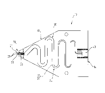
The embodiment, shown in Figure 1, of a contacting assembly according to the
invention 10 for the transmission of electrical signals in the form of a
measuring tip for
the measurement of devices under test with high frequency-circuits, for
example on
semiconductor wafers, comprises a carrier 12 with a circuit board which,
starting out
from a connection end 14, narrows gradually in the direction of a contact end
16.
Arranged on the carrier 12 is a conductor structure 20 which runs from the
connection
end 14 to the contact end 16.
The conductor structure 20 has at least one signal conductor and at least one
ground
conductor, whereby the ground conductor is arranged on the rear side, not
shown, of
the carrier 12, while the surface of the carrier 12 carrying the signal
conductor faces
the viewer in the represented figure. Alternatively or in addition, the
conductor
structure 20 can also possess several signal conductors. Alternatively, signal
and
ground conductors can be arranged on the same surface of the carrier 12.
A total of three spring-biased contact elements 22 in the form of contact
fingers 23
project from the contact end 16 of the carrier 12 beyond an edge of the
carrier for the
purpose of making contact with correspondingly-spaced contact points on the
device
under test. In the example shown, the middle contact finger 23 is connected
with the
signal conductor and the outer two contact fingers 23 are connected with the
ground
conductor. The outer contact fingers 23 are also ground contact elements 21.
Other
arrangements of the contact elements or more than three contact fingers are
also
conceivable.
A plug conductor 40 with an inner conductor and an outer conductor is arranged
at
the connection end 14 of the carrier 14. A coaxial cable or a mating plug
connector
can be plugged into the plug conductor 40 for further transmission of the HF
signals
picked up via the contact elements 22. The inner conductor of the plug
conductor 40
Date Recue/Date Received 2020-06-01
W02015/149893 9
PCT/EP2015/000044
is connected electrically with the signal conductor and thus with the middle
contact
finger 23, while the outer conductor of the plug conductor 40 is connected
electrically
with the ground conductor and thus with the two ground contact elements 21.
The conductor structure 20 has an impedance converter 24, whereby the
impedance
converter 24 has an electrical conductor segment 26 with a gradually widening
cross
section, starting out from the connection end 14 in the direction of the
contact end 16.
This conductor segment 26 is, in the embodiment shown, in the form of a
conductor
trace 27 of increasing width applied to the carrier 12. The conductor trace 27
is part
of the signal conductor which runs between the middle contact finger 23 and
the inner
conductor of the plug conductor 40. The geometrical form and the curvature of
the
conductor trace 26 are designed such that a Klopfenstein structure is created
for
impedance transformation between the connection end 14 and the contact end 16.
In
the example shown, signals can be picked up from a device under test through
the
contact finger 22 with a wave impedance of 12.5 0 and passed on free of
reflection
via a coaxial cable which is connected to the plug conductor 40 with a wave
impedance of 50 0. Thus, the illustrated contacting assembly 10 as a whole
represents an impedance converter in which the impedance transformation is
effected
by means of a Klopfenstein structure.
The contacting assembly 10 is configured to pick up and pass on HF signals
over a
frequency band from around 698 MHz to around 2.7 GHz without reflections
occurring, whereby the impedance level is raised from 12.5 0 at the contact
end 16
of the conductor structure 20 to 50 0 at the connection end of the conductor
structure
20. In this example this leads to a transformation ratio of 1:4.
Alternatively, the
impedance level can be raised from 10 0 at the contact end 16 to 50 0 at the
connection end, resulting in a transformation ratio of 1:5.
A more compact construction design of the contacting assembly 10 is possible
in that
the conductor trace 27 runs between the plug conductor 40 and the contact
finger 23
in a serpentine path includes several curves. The width of the conductor trace
27 at
the end of the conductor trace 27 facing the contact element 22 is around 4
times as
great as its width at the end facing the plug conductor 40. However, the form,
length
and curvature of the conductor trace 40 can be adjusted accordingly depending
on
Date Recue/Date Received 2020-06-01
WO 2015/149893 10
PCT/EP2015/000044
the impedance transformation which is to be achieved. The spacing and length
of the
contact elements 22 are designed such that the contact-side impedance is
matched
to the impedance of the component which is to be measured.
According to the invention, the impedance transformation is effected solely
through
the curvature of the conductor trace 27 of the signal conductor, without
additional
components such as SMDs being necessary. This means that the frequency band
can be broader and the contacting assembly according to the invention can thus
also
be used to test LTE components. The installation/incorporation of an SMD
component
is also unnecessary. The transformation ratio of the impedance converter can
be
varied individually and can for example 1:5, 5:1, 1:2, 2:1, 1:4, 4:1 etc.
Fig. 2 shows a second embodiment of a contacting assembly according to the
invention 10'. In this second embodiment the conductor segment 26' in the form
a
conductor trace 27' runs, not in a serpentine path, but in a linear path
starting out from
the connection end 14 to the contact end 16 via the carrier 12. The total
dimension of
the carrier, which substantially corresponds to the length of the conductor
trace 27',
which narrows in the direction of the connection end 14, is around 12 cm. The
straight
path of the conductor segment 26' prevents a crosstalk between individual
conductor
loops.
Unlike the first embodiment, the conductor structure 20 has a total of seven
contact
elements 22 projecting beyond an edge of the carrier 12, of which four ground
contact
elements 21 are each connected with a (common) ground conductor on the rear
side
of the carrier 12 and three signal-carrying contact elements are connected
with the
conductor trace 27'. The ground contact elements 21 and the signal-carrying
contact
elements thereby alternate. The two outer contact elements 22 are ground
contact
elements 21. Alternatively, more or less than seven contact elements 22 are
also
conceivable.
The illustrated branching into several contact elements connected with the
conductor
segment 26' minimises a reflection at the transition between the contact
elements 22
and the (wide) end of the conductor segment 26'. The spacing between the
individual
contact elements 22 can also be increased in this way while maintaining the
desired
Date Recue/Date Received 2020-06-01
WO 2015/149893 11
PCT/EP2015/000044
contact-side impedance. In the present case the spacing between two adjacent
contact elements 22 is more than 10 pm and the contact-side impedance around
10
O. The spacing between and number of the contact elements can be adjusted
accordingly depending on the desired impedance transformation.
Otherwise, reference is made to the explanations relating to the first
embodiment
shown in Fig. 1, which apply correspondingly to the second embodiment.
Date Recue/Date Received 2020-06-01
WO 2015/149893 12
PCT/EP2015/000044
List of reference numbers
10, 10' contacting assembly
12 carrier/circuit board
14 connection end
16 contact end
20 conductor structure
21 ground contact elements
22 contact elements
23 spring-biased contact finger
24 impedance converter
26, 26' conductor segment
27, 27' conductor trace
40 plug conductor
Date Recue/Date Received 2020-06-01