Note: Descriptions are shown in the official language in which they were submitted.
CA 02940941 2016-09-01
DIMMABLE MULTICHANNEL DRIVER FOR SOLID STATE LIGHT SOURCES
CROSS-REFERENCE TO RELAIED APPLICATION
[0001]
11CHNICAL FIELD
[0002] The present invention relates to lighting, and more specifically, to
electronic
circuits for solid state light sources.
BACKGROUND
[0003] A conventional light source such as, for example, an incandescent lamp
or
halogen lamp, when dimmed, acts like a near exact black body radiator and
follows
the Planckian curve on the 1931 CIE Chromaticity Diagram. For example, a
conventional incandescent lamp at its maximum output may output light having a
color temperature of 3000K. As that incandescent lamp is dimmed (e.g., through
use
of a triac dimmer), the current running through its filament is reduced,
resulting in a
lower, warmer color temperature (e.g., 2000K).
[0004] As solid state light sources become more widely used, lighting
designers and
lighting consumers desire that the solid state light sources behave similarly
to
conventional light sources. However, unlike an incandescent lamp or a halogen
lamp, solid state light sources typically hold their color temperature as they
are
dimmed. This behavior has been overcome to a degree by using a color mixing
technique. A two channel controllable current solid state light source driver
performs color mixing between two strings of solid state light sources to
achieve
incandescent-like dimming (i.e., dimming at or substantially near the
Planckian
CA 02940941 2016-09-01
WO 2013/166345 PCT/US2013/039371
curve), as desired by the market. An example of such a lamp is the Philips
Master
LEDspotMV GU10 Dim Tone lamp, which was designed to operate at 220V/230V
systems with a triac dimmer.
SUMMARY
[0005] At least one problem with the above-referenced Philips LED lamp is the
loss
of certain resistors in terms of efficiency, and the dependent LED current
control
based on the power transfer through the transformer. With these two resistors,
the
voltage across the two strings of solid state light sources (e.g., white LEDs
and amber
LEDs) can be equal, which does not force a string to turn off. For example, if
high
current is provided to the amber LED string, the loss of the resistor will be
significantly high. The circuit also does not have any feedback loop to the
primary
side of the transformer (e.g., to reduce or increase the energy transfer to
the
secondary side). Therefore, the current between two strings of solid state
light
sources needs to be shared according to the power transfer from the primary.
[0006] Embodiments overcome these and other deficiencies by providing a
dimmable multichannel driver for solid state light sources. Embodiments allow
at
least two solid state light source loads to be driven in a manner that allows
for
control of the current flowing through the solid state light source loads to
generate
illumination at a desired light color temperature.
[0007] In an embodiment, there is provided a power supply circuit. The power
supply circuit includes: a first drive circuit configured to generate a drive
current to
cause a first solid state light source load and a second solid state light
source load to
illuminate; a feedback and control circuit configured to receive feedback from
the
first solid state light source load and to control the drive current through
the first
solid state light source load based on the feedback; a second drive circuit
configured
to control the drive current through the second solid state light source load;
and a
master controller configured to provide a first input to the feedback and
control
circuit to control the drive current through the first solid state light
source load and a
second input to the second drive circuit to control the drive current through
the
second solid state light source load.
2
CA 02940941 2016-09-01
WO 2013/166345 PCT/US2013/039371
[0008] In a related embodiment, the first drive circuit may include a direct
current
(DC) to DC flyback converter circuit including a flyback converter controller.
In a
further related embodiment, the feedback and control circuit may be configured
to
compare a voltage corresponding to actual drive current through the first
solid state
light source load to a reference voltage and to control the first drive
circuit based on
the difference between the voltage corresponding to the actual drive current
and the
reference voltage.
[0009] In a further related embodiment, the feedback and control circuit may
include
an operational amplifier and an optical isolator configured to generate a
control
signal based on the difference between the voltage corresponding to the actual
drive
current and the reference voltage, and the flyback converter controller may be
configured to control the drive current generated by the first drive circuit
based on
the control signal.
[0010] In another further related embodiment, the feedback and control circuit
may
be configured to generate a voltage corresponding to the voltage across the
first solid
state light source load based on the actual drive current, and the master
controller
may be configured to adjust the reference voltage based on the voltage
corresponding to the voltage across the first solid state light source load.
[0011] In yet another further related embodiment, the first input may be a
first pulse
width modulation (PWM) signal to the feedback and control circuit to generate
the
reference voltage and the second input may be a second PWM signal to the
second
drive circuit. In a further related embodiment, the second drive circuit may
include
a DC to DC buck controller configured to control the drive current for the
second
solid state light source load based on the second PWM signal. In another
further
related embodiment, the power supply circuit may further include a front end
circuit
configured to generate a DC voltage based on an alternating current (AC)
input,
wherein the front end circuit may be further configured to provide the
generated DC
voltage to the first drive circuit. In a further related embodiment, the front
end
circuit and the first drive circuit may include a two stage low pass EMI
filter and
rectifier circuit. In another further related embodiment, the power supply
circuit
may further include a dimmer sense circuit configured to generate a dimmer
sense
3
voltage based on a phase cut voltage sensed in the DC voltage generated by the
front end circuit.
In a further related embodiment, a frequency of the first PWM signal and a
frequency of the
second PWM signal may each be selected from predetermined settings stored in
the master
controller, wherein the frequencies being selected are based on the dimmer
sense voltage. In a
further related embodiment, the first solid state light source load may
include solid state light
sources of a first color and the second solid state light source load may
include solid state light
sources of a second color, and the predetermined settings may be configured to
cause the first
solid state light source load and the second solid state light source load to
generate light, that
when combined, corresponds to a certain light color temperature.
[0012] In another embodiment, there is provided a method for operating a
dimmable
multichannel solid state light source drive system, comprising: determining if
a first solid state
light source load driven by a first drive circuit is illuminated based on a
voltage corresponding to
the voltage across the first solid state light source load generated in a
feedback and control
circuit; and controlling, via a master controller, the first drive circuit and
a second drive circuit,
such that: the first drive circuit is controlled based on the voltage
corresponding to the voltage
across the first solid state light source load by adjusting a reference
voltage in the feedback and
control circuit, wherein adjusting the reference voltage comprises adjusting a
first pulse width
modulation (PWM) signal provided to the feedback and control circuit to
generate the reference
voltage; and the second drive circuit drives a second solid state light source
load and is
controlled by providing a second PWM signal from the master controller,
wherein the second
PWM signal has a second duty cycle determined based on a dimmer sense voltage;
wherein a
current through the second solid state light source load is set, via the
controlled second drive
circuit, to a value less than a current through the first solid state light
source load, such that light
emitted by the first solid state light source load and the second solid state
light source load is
combined to result in a desired color temperature.
[0013] In a related embodiment, the first drive circuit comprises a DC to DC
flyback circuit
including a DC to DC flyback converter controller; and controlling may include
controlling the
DC to DC flyback circuit based on the voltage corresponding to the voltage
across the first solid
state light source load by adjusting the reference voltage in the feedback and
control circuit. In
another related embodiment, adjusting the reference voltage may include
adjusting a first pulse
width modulation (PWM) signal provided to the feedback and control circuit to
generate the
reference voltage. In a further related embodiment, the method may further
include receiving a
4
Date recue / Date received 2021-11-01
dimmer sense voltage from a dimmer sense circuit; determining a first duty
cycle for the first
PWM signal based on the dimmer sense voltage; and providing the first PWM
signal at the first
duty cycle to the feedback and control circuit. In a further related
embodiment, the method may
further include determining a second duty cycle for a second PWM signal based
on the dimmer
sense voltage; and controlling a second drive circuit configured to drive a
second solid state light
source load by providing the second PWM signal at the second duty cycle to the
second drive
circuit.
[0014] In a further related embodiment, controlling a second drive circuit may
include
controlling a DC to DC buck controller, the DC to DC buck controller being
configured to
control the drive current for the second solid state light source load based
on the second PWM
signal.
[0015] In another further related embodiment, determining the first duty cycle
and determining
the second duty cycle may include selecting a first frequency for the first
PWM signal and a
second frequency for the second PWM signal, wherein each frequency is selected
from
predetermined settings stored in a master controller, and wherein each
frequency is selected
based on the dimmer sense voltage. In a further related embodiment, the
predetermined settings
are configured to cause the first solid state light source load and the second
solid state light
source load to generate light, that when combined, corresponds to a certain
light color
temperature.
BRIEF DESCRIPTION OF THE DRAWINGS
[0016] The foregoing and other objects, features and advantages disclosed
herein will be
apparent from the following description of particular embodiments disclosed
herein, as
illustrated in the accompanying drawings in which like reference characters
refer to the same
parts throughout the different views. The drawings are not necessarily to
scale, emphasis instead
being placed upon illustrating the principles disclosed herein.
Date Recue/Date Received 2021-02-01
CA 02940941 2016-09-01
WO 2013/166345 PCT/US2013/039371
[0017] FIG. 1 shows a block diagram of a dimmable multichannel driver
according to
embodiments disclosed herein.
[0018] FIG. 2 illustrates a circuit diagram of a dimmable multichannel driver
according to embodiments disclosed herein.
[0019] FIG. 3 illustrates a circuit diagram of a front end circuit according
to
embodiments disclosed herein.
[0020] FIG. 4 illustrates a circuit diagram of a first solid state light
source drive
circuit according to embodiments disclosed herein.
[0021] FIG. 5 illustrates a circuit diagram of a dimmer sense circuit
according to
embodiments disclosed herein.
[0022] FIG. 6 illustrates a circuit diagram of a master controller according
to
embodiments disclosed herein.
[0023] FIG. 7 illustrates a circuit diagram of a feedback and control circuit
according
to embodiments disclosed herein.
[0024] FIG. 8 illustrates a circuit diagram of a second solid state light
source drive
circuit according to embodiments disclosed herein.
[0025] FIG. 9 illustrates a flowchart of a method of dimming solid state light
sources
according to embodiments disclosed herein.
DETAILED DESCRII51 ION
[0026] As used throughout, the term "solid state light source" includes light
sources
including, for example but not limited to, one or more light emitting diodes
(LEDs),
organic light emitting diodes (OLEDs), polymer light emitting diodes (PLEDs)
or
any other solid state device configured to emit light, and/or combinations
thereof.
Moreover, "solid state light source load" refers to an arrangement of one or
more
solid state light sources within another device (e.g., lamp, light engine,
fixture, etc.).
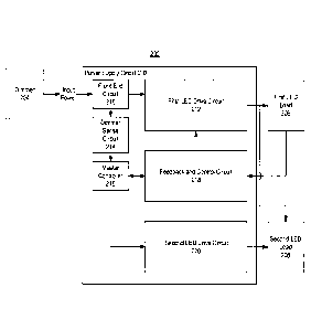
[0027] FIG. 1 is a block diagram of a dimmable multichannel driver system 200
that
includes a power supply circuit 202 configured to receive input power from a
dimmer 204 and to drive at least a first solid state light source load 206 and
a second
solid state light source load 208 (also referred to throughout as a first LED
load 206
and a second LED load 208). The power supply circuit 202 includes a front end
6
CA 02940941 2016-09-01
WO 2013/166345 PCT/US2013/039371
circuit 210, a first solid state light source drive circuit 212 (also referred
to
throughout as a first LED drive circuit 212), a dimmer sense circuit 214, a
master
controller 216, a feedback and control circuit 218, and a second solid state
light
source drive circuit 220 (also referred to throughout as a second LED drive
circuit
220). The dimmer 204 is not a core component of embodiments and thus is shown
as
optional in FIG. 1, but would be employed with some embodiments. For example,
in
some embodiments, the dimmer 204 includes an alternating current (AC) triac-
based
dimming circuit, configured as either a leading edge or a trailing edge
dimmer, or
both.
[0028] The front end circuit 210 may be, and in some embodiments is,
configured to
generate a DC voltage based on an input power (for example but not limited to
an
AC input voltage provided by the dimmer 204). The DC voltage generated by the
front end circuit 210 is then provided to at least the first LED drive circuit
212, which
is configured to generate a drive current for the first LED load 206 and the
second
LED load 208 based on the generated DC voltage. In some embodiments, the first
LED drive circuit 212 includes a DC to DC flyback converter circuit controlled
by a
flyback controller. In some embodiments, the dimmer sense circuit 214 is
configured
to determine a dimmer sense voltage based on the generated DC voltage. In some
embodiments, a phase cut voltage component present in the DC voltage causes
the
dimmer sense circuit 214 to generate the dimmer sense voltage. The dimmer
sense
voltage is then provided to the master controller 216. The master controller
216
senses a voltage generated by the feedback and control circuit 218 (e.g., a
voltage
corresponding to the voltage across the first LED load 206).
[0029] Based on the dimmer sense voltage and/or the voltage corresponding to
the
voltage across the first LED load 206, the master controller 216 is configured
to
provide a first input to the feedback and control circuit 218 and a second
input to the
second LED drive circuit 220. The first input, in some embodiments, is a first
PWM
signal configured to cause the feedback and control circuit 218 to generate a
reference voltage. In some embodiments, the feedback and control circuit 218
is
configured to generate a voltage corresponding to the actual drive current
through
the first LED load 206, and to compare this voltage to the reference voltage.
The
7
CA 02940941 2016-09-01
WO 2013/166345 PCT/US2013/039371
resulting difference between the voltage corresponding to the actual drive
current
and the reference voltage is provided to the first LED drive circuit 212. In
some
embodiments, the difference serves as one or more control signals to the
flyback
controller of the first LED drive circuit 212, the flyback controller being
configured to
control the first LED drive circuit 212 based on one or more the control
signals. The
second PWM signal is provided to the second LED drive circuit 220. In some
embodiments, a buck controller in the second LED drive circuit 220 is
configured to
control the current flowing through the second LED load 208 based on the
second
PWM signal. More specifically, the drive current for the second LED load 208
is
provided by the first LED drive circuit 212, however, current flow through the
second LED load 208 may be, and in some embodiments is, controlled by the
second
LED drive circuit 220. For example, the current flow through the second LED
load
208, in some embodiments, is restricted to be less than the current flow
through the
first LED load 206, so that the second LED load 208 appears dimmer than the
first
LED load 206. This results in a desired color temperature for the combined
light
emitted by both the first LED load 206 and the second LED load 208.
[0030] In this regard, the frequencies of the first PWM signal and the second
PVVIVI
signal may be, and in some embodiments are, selected from predetermined
settings
in the master controller 216 based on, for example but not limited to, the
dimmer
sense voltage and/or the voltage corresponding to the voltage across the first
LED
load 206. In some embodiments, the dimmer sense voltage provides a baseline
amount of light output that is desired (e.g., as dictated by the setting of
the dimmer
204), and this baseline amount may be adjusted to account for actual device
performance based on feedback (e.g., the voltage across the first LED load
206). In
some embodiments, the dimmer sense voltage is scaled by the master controller
216
to a digital value between, for example, 0 and 255 that is then used in
selecting a
record from a predetermined data array (e.g., also stored in the master
controller
216). Each record in the data array corresponds to a "recipe" for generating a
desired light color temperature from the combined light output of the first
LED load
206 and the second LED load 208. A first value in the record may be the
digital
dimmer value, while a second value in the record may correspond to the first
PWM
8
CA 02940941 2016-09-01
WO 2013/166345 PCT/US2013/039371
signal duty cycle, and a third value in the record may correspond to the
second
PWIvl signal frequency.
[0031] FIG. 2 is a circuit diagram of a power supply circuit 202'. Note that
the circuit
diagrams provided in FIGs. 2-8 have been provided merely for the sake of
explanation herein, and are not intended to limit any of the disclosed
embodiments
to implementation using the only the depicted components in the depicted
configuration. Similar to FIG. 1, the power supply circuit 202' comprises a
front end
circuit 210', a first LED drive circuit 212', a dimmer sense circuit 214', a
master
controller 216', a feedback and control circuit 218', and a second drive
circuit 220'.
The power supply circuit 202' may be configured to drive any number of loads,
though in FIG. 2 it is shown as being configured to drive two loads (the first
LED
load 206 and the second LED load 208). In embodiments where loads include
different colored solid state light sources (e.g., the first LED load 206
includes at least
one white solid state light source and the second LED load 208 includes at
least one
amber solid state light source), the current through each load may be, and in
some
embodiments is, controlled to create combined output light of a certain color
temperature. In addition, the power supply circuit 202' has a very high power
factor
(e.g., is very efficient), has low total harmonic distortion (THD) (e.g., has
good
isolation from noise), and supports both leading and trailing edge dimmers.
The
power supply circuit 202' also has an output isolated for safe operation to
meet
Underwriter's Laboratories (UL) class 2 operational requirements. The
functionality
associated with each illustrated circuit 210'-220' are described further
herein with
respect to FIGs. 3-8.
[0032] FIG. 3 is a circuit diagram of the front end circuit 210' shown in FIG.
2. The
front end circuit 210' includes, for example but not limited to, a fuse Fl, a
metal
oxide varistor (MOV) 0, resistors R1-R3 and R14, capacitors C3-C4, inductors
L1-L2,
and a bridge D8. An AC voltage (e.g., from the dimmer 204 of FIG. 1) is
supplied to
inputs J1 and J2. The fuse Fl is connected, on one side, to the input J1, and
on its
other side, to the MOV 0, to the resistor R3, and to the parallel combination
of the
inductor L1 and the resistor Rl. The MOV 0 is also connected to the input J2.
The
resistor R3 is also connected to the capacitor C4, which is also connected to
the input
9
CA 02940941 2016-09-01
WO 2013/166345 PCT/U52013/039371
J2. The input J2 is also connected to the parallel combination of the resistor
R2 and
the inductor L2. The resistor R14 is connected in series with the capacitor
C3. The
capacitor C3 is connected to the parallel combination of the resistor R2 and
the
inductor L2, and to the bridge D8. The resistor R14 is connected to the
parallel
combination of the inductor L1 and the resistor R1, and to the bridge D8 (at
pin 4).
The components in the front end circuit 210', with the exception of the bridge
D8, are
configured to stabilize the input power and protect against interference from,
for
example, voltage spikes (e.g., from electrostatic discharge (ESD), lightning,
etc.),
electromagnetic interference (EMI), etc. The bridge DS may be, and in some
embodiments is, a bridge rectifier configured to rectify the incoming AC
voltage into
a DC voltage usable by the remainder of the power supply circuit 202'. The
bridge
D8, at pin 2, is connected to a GND_PWR, and at pin 1, is connected to the
first LED
drive circuit 212'.
[0033] FIG. 4 is a circuit diagram of the first LED drive circuit 212'. The
first LED
drive circuit 212' includes, for example but not limited to, resistors R4-R10,
R12, and
R33, capacitors C1-C2, C7, and C10-C12, an inductor L3, diodes DI-D3, a
transformer Ti, a transistor Q1, a Zener diode G, and a controller U1. Many of
the
components configured around the controller U1 may, and in some embodiments
do, vary depending on the selected type of controller. The controller Ul shown
in
FIG. 4 and described herein is a L6562D Transition Mode PFC controller
manufactured by ST Microelectronics Inc., though of course other controllers
may
be, and in some embodiments are, used. The controller U1 shown in FIG. 1
includes
eight pins, numbered 1-8. Pin 6, the ground pin, is connected to ground. The
remaining pins are as described herein.
[0034] The inductor L3 and the resistor R4 are each connected to the output
pin 1 of
the bridge D8 of the front end circuit 210' of FIG. 3. The resistor R4 is also
connected
to pin 3 of the controller U1 and to the resistor R5. The resistor R5 is also
connected
to ground. The inductor L3 is also connected to the capacitor C10, which is
also
connected to ground, and to the resistor R6, the parallel combination of the
resistor
R18 and the capacitor C11, and a primary winding (pin 5) of the transformer
Ti. The
inductor L3 and the capacitor C10, along with the inductors L1 and L2, the
resistor s
CA 02940941 2016-09-01
WO 2013/166345 PCT/US2013/039371
R3 and R14, and the capacitors C3 and C4 shown in FIG. 3, together operate as
a two
stage low pass EMI filter. The two stage low pass EMI filter is unique in that
it may,
and in some embodiments does, also damp ringing associated with triac dimmers.
In some embodiments, the values for the components in the two stage low pass
EMI
filter are also chosen to adjust the phase angle between the input voltage and
input
current, which may result in low TI-ID. One reason EMI may be so low with this
configuration is that switching frequency is constantly changing, which
spreads the
noise over a wide band. The DC voltage generated by the front end circuit 210'
at
pin 1 of the bridge D8 is reduced via a voltage divider including the
resistors R4 and
R5, before being supplied to a multiplier input pin of the controller U1
(i.e., pin 3).
The DC voltage is also provided to the primary winding (pins 5 and 6) of the
transformer T1. The transformer Ti also includes secondary and bias windings.
The
turn ratio between the secondary and bias windings of the transformer Ti
determines the bias voltage based upon the type of solid state light source
selected
for the first LED load 206 and the second LED load 208. Tight coupling between
the
primary winding and the secondary winding may be considered when selecting the
transformer Ti to avoid losses due to leakage inductance. The parallel
combination
of the resistor R18 and the capacitor C11 are also connected in series with
the diode
D3, across the primary winding of the transformer Ti. This helps to perpetuate
the
"flyback" response of thje first LED drive circuit 212'.
[0035] The capacitors C14, Cl, and C7 are connected in parallel with each
other. The
parallel combination of the capacitors C14, C1, and C7 is connected to ground,
on
one side, and to the resistor R6, a VCC+ input, and a cathode of the diode D2
on the
other side. An anode of the diode D2 is connected to the resistor R12, which
itself is
connected to a cathode of the diode DI and to the capacitor C2. The capacitor
C2 is
also connected to ground. An anode of the diode D1 is connected to an AUX
input.
The VCC+ input is also connected to a VCC input pin (pin 8) of the controller
U1.
[0036] The resistor R7 is connected to an INV input. The resistor R7 and the
capacitor C12 are connected in series. The series combination of the resistor
R7 and
the capacitor C12 are connected in parallel with the resistor R8, and both are
connected, on one side, to an inverting input pin (pin 1) of the controller U1
and, on
11
CA 02940941 2016-09-01
WO 2013/166345 PCT/US2013/039371
the other side, to a compertstation input pin (pin 2) of the controller U1. A
CS input
is connected to a PWM comparator input pin (pin 4) of the controller U1.
[0037] A gate driver output pin (pin 7) of the controller Ul is connected to
the
resistor R9. The resistor R9 is also connected to a gate of the transistor Q1,
which has
the Zener diode G across the gate and a source. A drain of the transistor Q1
is
connected to the primary winding (pin 5) of the transformer T1. The source of
the
transistor Q1 is also connected to the parallel combination of the resistors
R10 and
R33. The parallel combination of the resistors R10 and R33 is connected, on
one side,
to ground, and on the other side, in addition to the source of the transistor
QL to the
CS input.
[0038] A zero current detector input (pin 5) of the controller U1 is connected
to the
resistor R13. The resistor R13 is also connected to the AUX input and to the
feedback
winding (pin 2) of the transformer Ti, which is also connected to ground (at
pin 1).
[0039] At startup, the controller U1 receives two signals at the multiplier
pin (pin3)
and the VCC input pin (pin 8). The voltage at the VCC input pin (pin 8) begins
to
increase from zero as the capacitors Cl, C7, and C14 begin to charge with
current
supplied by the DC voltage generated by the front end circuit 210' through the
resistor R6. The controller U1 then starts supplying pulses to the transistor
Q1 from
the gate driver output pin (pin 7) through the resistor R9, forcing current
into the
primary winding of the transformer Ti through the transistor Q1. When the
transistor Q1 turns off, the feedback winding (pins 1-2) of the transformer Ti
"flyback" and supply current through the diodes D1 and D2, charging the
capacitors
Cl, C2, C7, and C14. That is, the first LED drive circuit 212' starts
generating VCC
internally. The controller U1 is reset by monitoring the voltage on the zero
current
detector input pin (pin5) of the controller Ul through the resistor R13. The
current
through the transistor Q1 is limited by the combination of the voltage at the
multiplier input pin (pin3) of the controller U1 and a voltage produced by an
error
amplifier configured between the inverting and compensation inputs of
controller
U1 (pins 1 and 2, respectively). The error amplifier, which includes the
resistors R7
and R8 and the capacitor C12, as described above, acts as a compensation
network to
achieve stability in the voltage control loop and to ensure high power factor
and low
12
CA 02940941 2016-09-01
WO 2013/166345 PCT/US2013/039371
THD. In some embodiments, the power output of the first LED drive circuit 212'
is
set by the resistors R10 and R33, which are coupled to the PVVM comparator
input
pin of the controller Ul (pin 4), as described above.
[0)40] FIG. 5 is a circuit diagram of the dimmer sense circuit 214'which
includes, for
example, a two-diode package D5, a diode D7, resistors R27-R29 and R35-R37,
and a
transistor Q2. The two-diode package D5 is connected to the secondary winding
of
the transformer Ti of the first LED drive circuit 212' shown in FIG. 4. The
capacitor
C17 is connected in series with the resistor R27. The resistor R28 is
connected across
the series connection of the capacitor C17 and the resistor R27. On one side,
the
parallel combination of the resistor R28 with the resistor R27 and the
capacitor C17 is
connected to a GND_SIGNAL, and on the other side, to the two-diode package D5.
The resistors R27-R29 and the capacitor C17 behave as a triac sensing circuit,
that
receives the voltage signal from the secondary winding of the transformer Ti.
Once
a dimmer 204 is connected at the primary AC input (e.g., the inputs J1 and J2
of the
front end circuit 210' shown in FIG. 3), the phase cut voltage waveform will
occur
across the primary winding of the transformer Ti. A voltage waveform of the
same
shape (e.g., a phase cut waveform) will also occur across the secondary
winding of
the transformer Ti through the winding ratio of the transformer Ti. The triac
sensing circuit will average those phase cut waveforms into a DC voltage
(e.g., the
dimmer sense voltage), which is provided as a reference signal to the master
controller 216/216'. A change in the phase of the input voltage will cause an
image
change in the dimmer sense voltage.
[0041] The two-diode package D5 is also connected to the resistor R35. The
resistor
R35 is also connected to a cathode of the diode D7 and to a base of the
transistor Q2.
An anode of the diode D7 and the resistor R36 are connected to the GND SIGNAL.
The resistor R36 is also connected to an emitter of the transistor Q2, and to
a
VCC_SEC output. The resistor R37 is connected between a collector of the
transistor
Q2 and an OUT output. Thus, the two-diode package D5 is configured to block
current from flowing back into the secondary winding of the transformer T1 of
the
first LED drive circuit 212'. The resistors R35-R37, the diode D7, and the
transistor
13
CA 02940941 2016-09-01
WO 2013/166345 PCT/US2013/039371
Q2 are configured to regulate an operational voltage (VCC) for the master
controller
216' and the second LED drive circuit 220'.
[0042] FIG. 6 is a circuit diagram of the master controller 216'. In FIG. 6,
the master
controller 216' is an ATtiny261A microcontroller manufactured by the Atmel
Corporation, however, embodiments are not limited to implementation using only
this microcontroller. Components configured around, or coupled to, the master
controller 216', but not specifically described herein, may be particular to
the
operational requirements of the ATtiny261A. As stated above, VCC may be
supplied to the master controller 216' by the dimmer sense circuit 214', via
the
VCC_SEC output. After VCC increases to a level sufficient for activation, the
master
controller 216' proceeds to execute instructions stored within a memory of the
master controller 216'. In some embodiments, these instructions provide for
the
control of the first LED load 206 and the second LED load 208 based on, for
example,
the dimmer sense voltage. Examples of operation wherein the master controller
216'
controls these loads are described further in regard to FIGs. 7-9. The master
controller 216' includes a number of pins, some of which have no connections
in
embodiments of the present invention. In FIG. 6, pin 21 is connected to the
GND_SIGNAL, pin 2 is connected to a PB3_BUCK, pin 4 is connected to the
VCC_SEC output, pin 26 is connected to a PAO, and pin 25 is connected to a PAL
Pins 10 and 11 are connected to each other, and to a resistor R39. The
resistor R39 is
also connected to a RESET pin and a RESET. Pin 15 is connected to a
PA5_LEDSENSE. Pin 18 is connected to the VCC SEC output and to a VCC, as well
as to a capacitor C13. The capacitor C13 is also connected to pin 33, which is
also
connected to the GND_SIGNAL. Pin 31 is connected to a PB1_VREF and to a
resistor R40. The resistor R40 is also connected to a PB1_MISO and to a MISO
input.
Pin 5 is connected to a GND and to the GND_SIGNAL. Pin 32 is connected to the
PB1 and to a resistor R34. The resistor R34 is also connected to an SCK input
and to
an SCK. Pin 30 is connected to the PAD and to a resistor R11. The resistor R11
is
connected to the MISO input and to an MOSI.
10043] FIG. 7 is a circuit diagram of a feedback and control circuit 218'. The
feedback
and control circuit 218' includes, for example, a diode D4, operational
amplifiers
14
CA 02940941 2016-09-01
WO 2013/166345 PCT/US2013/039371
(a.k.a. "op-amps") U3-A, U3-B, and U3-C, capacitors C5, C15, and C19-C20, an
optoisolator U2, resistors R15, R17, R19, R21, R23-R25, and R31-R32. An anode
of the
diode 04 is connected to the transformer Ti of the first LED drive circuit
212'. A
cathode of the diode 04 is connected to the op-amp U3-C, to the capacitor C5,
to the
resistor R32, to the OUT output, and a terminal J3. The capacitor C20 is
connected
across the op-amp U3-C, and is connected to the GND_SIGNAL. The capacitor C5
is
also connected to ground, to the transformer Ti, and to the resistor R15. The
resistor
R15 is also connected to a terminal J4 and to the resistor R23. The resistor
R32 is also
connected to the resistor R20 and to the resistor R31. The resistor R31 is
also
connected to the capacitor C8 and to GND_SIGNAL. The capacitor C8 is also
connected to the resistor R20 and to the PA5_LEDSENSE. The resistor R23 is
also
connected to the resistor R21 and to an inverting input of the op-amp U3-A.
The
resistor R21 is also connected to the capacitor C15. The capacitor C15 is also
connected to an output of the op-amp U3-A and to a cathode of the optoisolator
U2.
The resistor R17 is connected to the PB1_VREF and to the resistor R25 and to
the
capacitor C19. The capacitor C19 is connected to the resistor R24 and to the
GND_SIGNAL. The resistor R24 is connected to the resistor R25, and both are
connected to a non-inverting input of the op-amp U3-A. An anode of the
op toisolator U2 is connected to the resistor R22. The resistor R22 is also
connected to
the OUT output. The resistor R30 is connected to the INV input and to the
resistor
R19 and to the optoisolator U2. The resistor R19 is also connected to the
GND_PVVR.
The optoisolator U2 is also connected to the VCC+ input.
[0044] The first LED load 206 and the second LED load 208 are coupled to the
terminal J3 of the feedback and control circuit 218', with the current for
driving both
loads being supplied by the diode D4. The capacitor C5 is configured to reduce
the
voltage swing on the first LED load 206 and the second LED load 208, and
provides
power to the op-amp U3-C as well as to the second LED drive circuit 220'. The
resistors R20, R31, and R32 and the capacitor C8 are configured to operate as
a
voltage sensing circuit by generating a voltage corresponding to the voltage
across
the first LED load 206. The resistors R17, R24, and R25, and the capacitor C19
are
configured to generate a DC reference voltage to the non-inverting input of
the op-
CA 02940941 2016-09-01
WO 2013/166345 PCTAIS2013/039371
amp U3-A (pin 3). In some embodiments, the master controller 216' monitors the
voltage corresponding to the voltage across the first LED load 206 generated
by the
voltage sensing circuit, makes a determination as to whether the voltage
across the
first LED load 206 requires adjustment (e.g., if the voltage is too low to
generate the
desired light output from the first LED load 206), and if determined to be
required,
adjusts a first PVVM signal being provided by the master controller 216'
(e.g., from
the PB1_VREF) to the reference voltage circuit, which generates the reference
voltage
based on the first PWM signal.
[0045] The first LED load 206 may be, and in some embodiments is, further
coupled
to the terminal J4 in the feedback and control circuit 218'. In some
embodiments, the
first LED load 206 includes a string of solid state light sources connected
between the
terminals J3 and J4. The drive current flowing through first LED load 206
(e.g., in
through the terminal J3 and out to the terminal J4) is then directed to flow
through
the resistor R15. The resistor R15 serves as a current sensing resistor. The
voltage
across the resistor R15 is compared to the reference voltage on the non-
inverting
input of the op-amp U3-A, the operation of which is stabilized by a negative
feedback loop including the resistors R2 and R23 and the capacitor C15. The
output
of the op-amp-U3-A (pin 1) determines the on-off operation of the optoisolator
U2.
For example, when the output of the op-amp U3-A is low, current flows through
the
solid state light source inside the optoisolator U2, causing the solid state
light source
to illuminate and to send a signal across to a primary side of the
optoisolator U2.
This on-off signal sends a message to the INV input, which is connected to pin
1 of
the controller U1 in the first LED drive circuit 212' to start or stop sending
power to
the secondary of the transformer T1. In this manner, the drive current flowing
to the
first LED load 206 and to the second LED load 208 is controlled.
[0046] FIG. 8 is a circuit diagram of the second LED drive circuit 220', which
includes, for example, capacitors C6, C16, and C21, an inductor L4, resistors
R16,
R26, R38, a diode D6, and a controller U5. In FIG. 8, the controller U5 is an
LM3414
buck controller manufactured by National Semiconductor Corporation, though of
course other controllers may be, and in some embodiments are, used. As stated
above, components configured around, or coupled to, the controller U5, but not
16
CA 02940941 2016-09-01
WO 2013/166345 PCT/1152013/039371
specifically described herein, may be particular to the operational
requirements of
the LM3414. The controller U5 has eight pins. Pin 5 is connected to a resistor
R26.
The resistor R26 is also connected to the GND_SIGNAL. Pin 6 is connected to a
resistor R38. The resistor R38 is connected to the PB3_BUCK. Pin 54 is
connected
directly to GND_SIGNAL. Pin 3 is connected to a resistor R16. The resistor R16
is
also connected to GND SIGNAL. Pin 2 is connected to ground. Pin 1 is connected
to the VCC_SEC and to the capacitor C6. The capacitor C6 is also connected to
GND_SIGNAL. Pin 81s connected to a cathode of a diode D6, to the capacitor
C21,
to the capacitor C16, and to the output OUT. The capacitor C16 is also
connected to
ground. The capacitor C21 is also connected to a terminal J6. Pin 7 is
connected an
anode of the diode D6 and to the inductor L4. The inductor L4 is connected to
the
capacitor C21 and to the terminal J6. In some embodiments, the second LED load
208 is a string of solid state light sources coupled to (and receiving drive
current
from) the terminal J3 in the feedback and control circuit 218'. The other end
of the
second LED load 208 is coupled to the terminal J6 of the second LED drive
circuit
220', allowing the second LED drive circuit 220' to control the flow of the
drive
current. Operational voltage generated by the resistors R35, R36, and R37, the
diode
D7, and the transistor Q2 in the dimmer sense circuit 214' is provided as VCC
to the
controller U5 via the OUT output connected to pin 8. In some embodiments, on
activation of the power supply circuit 202', VCC will increase to a level
allowing the
controller U5 to activate, which causes the controller U5 to switch on an
internal
MOSFET (not shown in FIG. 8) and to start drawing drive current from the
second
LED load 208 through the inductor L4. Once the internal MOSFET inside the
controller U5 turns off, the energy stored in the inductor L4 will discharge
through
the diode D6 and supply the current to the second LED load 208. Thus, the
drive
current flowing through the second LED load 208 will be controlled by the
switching
operation of the controller U5. The switching of the controller U5 may, in
turn be
controlled by a second PVVIVI signal generated by the master controller 216'
to pin 6
on the controller U5 (via the PB3_BUCK). For example, altering the duty cycle
of the
second PWM signal may reduce or increase the amount of drive current allowed
to
flow through the second LED load 208. In this manner, output characteristics
of
17
CA 02940941 2016-09-01
WO 2013/166345 PCT/US2013/039371
second LED load 208, such as but not limited to brightness, may be controlled
as a
percentage of the output characteristics, such as but not limited to
brightness, of the
first LED load 206. When the first LED load 206 and the second LED load 208
contain solid state light sources of different colors (for example but not
limited to
white solid state light sources and amber solid state light sources), the
light output of
each load may be controlled to generate a desired combined light color
temperature.
[0047] In some embodiments, the master controller 216' is configured to
determine
the setting of the dimmer 204 based on the dimmer sense voltage provided by
the
dimmer sense circuit 214'. The master controller 216' then generates a first
PVVM
signal to set the reference voltage in the feedback and control circuit 218'
and a
second PVVM to control the second LED drive circuit 220'. In the event of very
low
current flowing through the first LED load 206, the master controller 216' may
detect
the situation through a drop in voltage corresponding to the voltage across
the first
LED load 206 (as generated in the feedback and control circuit 218'), and may
then
set a new reference voltage that causes the first LED drive circuit 212' to
generate
more drive current. In this manner, the first LED load 206 may be prevented
from
inadvertently turning off. In the event of start-up, the master controller
216' may
detect a low voltage corresponding to the voltage across the first LED load
206 and
may set a new reference voltage to generate more power from the first LED
drive
circuit 212'. After the voltage corresponding to the voltage across the first
LED load
206 rises above the reference voltage, the master controller 216' may sense
the
dimmer setting and may determine the current of both the first LED load 206
and the
second LED load 208 as a continuous loop.
[0048] FIG. 9 illustrates a flowchart of operations for a dimmable
multichannel solid
state light source drive/power system, as described throughout. Following
startup
in operation 900, a master controller in a power supply circuit is configured
to
determine whether a first LED load is illuminated. The determination of
whether
the first LED load is illuminated is based on, for example but not limited to,
a
voltage generated by feedback and control circuit in the power supply circuit,
the
voltage corresponding to the voltage across the first LED load, which may be
generated in a feedback and control circuit, as described above. If in
operation 902 it
18
CA 02940941 2016-09-01
WO 2013/166345 PCT/US2013/039371
is determined that the first LED load is not illuminated, then in operation
904 the
master controller may adjust a reference voltage. For example, the master
controller
may increase the duty cycle of a first PWM signal, which may cause the
reference
voltage to increase in the feedback and control circuit. The increase in
reference
voltage may cause first LED drive circuit in the power supply circuit to
generate
more drive current for illuminating the first LED load.
[0049] If in operation 902 it is determined that the first LED load is
illuminated, then
in operation 905, the master controller receives a dimmer sense voltage. The
dimmer
sense voltage is generated by a dimmer sense circuit in the power supply
circuit, and
may correspond to the setting of an AC dimmer coupled to the power supply
circuit.
In operation 908, the master controller determines inputs based on the dimmer
sense
voltage. For example, the master controller may be configured to select inputs
(e.g.,
duty cycle settings for PWM signals) from predetermined settings in the master
controller based on the dimmer sense voltage. In operation 910, the master
controller provides the inputs determined in operation 908 to, for example,
the
feedback and control circuit and/or the second LED drive circuit in the power
supply circuit. The inputs may be, for example, first and second PWM signals.
Operation 910 may then be followed by a return to operation 900 to restart the
flow
of operations.
[0050] While FIG. 9 illustrates various operations according to embodiments,
it is to
be understood that not all of the operations depicted in FIG. 9 are necessary
for other
embodiments. Indeed, it is fully contemplated herein that in other
embodiments, the
operations depicted in FIG. 9, and/or other operations described herein, may
be
combined in a manner not specifically shown in any of the drawings, but still
fully
consistent with the present disclosure. Thus, claims directed to features
and/or
operations that are not exactly shown in one drawing are deemed within the
scope
and content of the present disclosure.
[0051] The methods and systems described herein are not limited to a
particular
hardware or software configuration, and may find applicability in many
computing
or processing environments. The methods and systems may be implemented in
hardware or software, or a combination of hardware and software. The methods
19
CA 02940941 2016-09-01
WO 20131166345 PCT/U52013/039371
and systems may be implemented in one or more computer programs, where a
computer program may be understood to include one or more processor executable
instructions. The computer program(s) may execute on one or more programmable
processors, and may be stored on one or more storage medium readable by the
processor (including volatile and non-volatile memory and/or storage
elements),
one or more input devices, and/or one or more output devices. The processor
thus
may access one or more input devices to obtain input data, and may access one
or
more output devices to communicate output data. The input and/or output
devices
may include one or more of the following: Random Access Memory (RAM),
Redundant Array of Independent Disks (RAID), floppy drive, CD, DVD, magnetic
disk, internal hard drive, external hard drive, memory stick, or other storage
device
capable of being accessed by a processor as provided herein, where such
aforementioned examples are not exhaustive, and are for illustration and not
limitation.
[0052] The computer program(s) may be implemented using one or more high level
procedural or object-oriented programming languages to communicate with a
computer system; however, the program(s) may be implemented in assembly or
machine language, if desired. The language may be compiled or interpreted.
[0053] As provided herein, the processor(s) may thus be embedded in one or
more
devices that may be operated independently or together in a networked
environment, where the network may include, for example, a Local Area Network
(LAN), wide area network (WAN), and/or may include an intranet and/or the
internet and/ or another network. The network(s) may be wired or wireless or a
combination thereof and may use one or more communications protocols to
facilitate
communications between the different processors. The processors may be
configured for distributed processing and may utilize, in some embodiments, a
client-server model as needed. Accordingly, the methods and systems may
utilize
multiple processors and/or processor devices, and the processor instructions
may be
divided amongst such single- or multiple-processor/devices.
[0054] The device(s) or computer systems that integrate with the processor(s)
may
include, for example, a personal computer(s), workstation(s) (e.g., Sun, HP),
personal
CA 02940941 2016-09-01
WO 2013/166345 PCT/US2013/039371
digital assistant(s) (PDA(s)), handheld device(s) such as cellular
telephone(s) or
smart cellphone(s), laptop(s), handheld computer(s), or another device(s)
capable of
being integrated with a processor(s) that may operate as provided herein.
Accordingly, the devices provided herein are not exhaustive and are provided
for
illustration and not limitation.
[0055] References to "a microprocessor" and "a processor", or the
microprocessor"
and "the processor,'' may be understood to include one or more microprocessors
that
may communicate in a stand-alone and/or a distributed environment(s), and may
thus be configured to communicate via wired or wireless communications with
other processors, where such one or more processor may be configured to
operate on
one or more processor-controlled devices that may be similar or different
devices.
Use of such "microprocessor'' or ''processor" terminology may thus also be
understood to include a central processing unit, an arithmetic logic unit, an
application-specific integrated circuit (IC), and/or a task engine, with such
examples
provided for illustration and not limitation.
[0056] Furthermore, references to memory, unless otherwise specified, may
include
one or more processor-readable and accessible memory elements and/or
components that may be internal to the processor-controlled device, external
to the
processor-controlled device, and/or may be accessed via a wired or wireless
network using a variety of communications protocols, and unless otherwise
specified, may be arranged to include a combination of external and internal
memory devices, where such memory may be contiguous and/or partitioned based
on the application. Accordingly, references to a database may be understood to
include one or more memory associations, where such references may include
commercially available database products (e.g., SQL, Informix, Oracle) and
also
proprietary databases, and may also include other structures for associating
memory
such as links, queues, graphs, trees, with such structures provided for
illustration
and not limitation.
[0057] References to a network, unless provided otherwise, may include one or
more
intranets and/or the Internet. References herein to microprocessor
instructions or
21
CA 02940941 2016-09-01
WO 2013/166345 PCT/US2013/039371
microprocessor-executable instructions, in accordance with the above, may be
understood to include programmable hardware.
[0058] Unless otherwise stated, use of the word "substantially" may be
construed to
include a precise relationship, condition, arrangement, orientation, and/or
other
characteristic, and deviations thereof as understood by one of ordinary skill
in the
art, to the extent that such deviations do not materially affect the disclosed
methods
and systems.
[0059] Throughout the entirety of the present disclosure, use of the articles
"a"
and/or "an" and/or "the" to modify a noun may be understood to be used for
convenience and to include one, or more than one, of the modified noun, unless
otherwise specifically stated. The terms "comprising", "including'' and
"having" are
intended to be inclusive and mean that there may be additional elements other
than
the listed elements.
[0060] Elements, components, modules, and/or parts thereof that are described
and/or otherwise portrayed through the figures to communicate with, be
associated
with, and/or be based on, something else, may be understood to so communicate,
be
associated with, and or be based on in a direct and/or indirect manner, unless
otherwise stipulated herein.
[0061] Although the methods and systems have been described relative to a
specific
embodiment thereof, they are not so limited. Obviously many modifications and
variations may become apparent in light of the above teachings. Many
additional
changes in the details, materials, and arrangement of parts, herein described
and
illustrated, may be made by those skilled in the art.
22