Note: Descriptions are shown in the official language in which they were submitted.
CA 02940993 2016-08-26
WO 2015/128551 PCT/F12015/050123
1
Switched-mode converter and method for converting electrical energy
Field of invention
The present invention relates generally to switched-mode converters of
electric
power. More specifically, the present invention relates to what is disclosed
in the
preambles of the independent claims. The invention has advantageous
applications especially in power supplies of electrical devices.
Background
Power supplies, such as switching power supplies, are used for providing
direct
current (DC) supply for various electronic devices. Such power supplies may be
connected at the electrical power input of a device, or they may convert power
for
a specific part of a device, for example. Power supplies are nowadays usually
implemented with switched-mode converters. The input of a switched-mode
converter may be AC or DC current, and input/output voltages vary according to
the implementation. While most electronic devices have switched-mode power
supplies for providing the operating power it is essential that the switched-
mode
converters have a good efficiency.
Switched-mode converters use input current for charging energy to an inductor
in
one phase, and in another phase the charged energy is led to load. These
operating phases are switched with high frequency. The basic structures of
switched power supplies include boost-type converters which increase the
voltage, and buck-type converters which decrease the voltage. In the boost
type
power supply the input power is led to the load with an inductor, wherein a
transistor connects the inductor directly to the input voltage in a first
phase for
loading energy to the inductor, and in a second phase the charged inductor is
connected to the load for supplying energy with higher voltage. In the buck-
type
converter a current flows continuously in the circuit of an inductor and a
load A
transistor sequentially connects the input voltage to the circuit thus
increasing the
energy of the inductor in a first phase, for being used in the load in a
second
phase.
Additionally there exist combinations of the basic switched-mode converter
types,
such as converters based on resonance, and cascade-type converters for
CA 02940993 2016-08-26
WO 2015/128551 PCT/F12015/050123
2
increasing voltage. Simple switched-mode power supplies typically have
efficiency between 70% and 90%. For example, nominal efficiency of a boost-
type
power supply is typically 70% and efficiency of a buck-type power supply is
typically 80-90%. There are also power supplies with higher efficiencies, such
as
split-pi type switch power supplies where several transistors are used for
connecting the input energy source to feed several inductors sequentially so
that
the current from the input voltage source is almost even. This minimizes
losses
caused by current changes and current spikes, and it is possible to achieve
efficiencies that are higher than 90%. However, this solution leads to a more
.. complicated structure and therefore higher production costs.
The following two documents disclose interleaved converters with two
sequentially
switched, parallel inductors: Taufik Taufik, Tadeus Gunawan, Dale Dolan and
Makbul Anwari, Documents Design and analysis of two-phase boost DC-DC
converter World Academy of Science, Engineering and Technology, issue 43,
2010, and Mounica Ganta, PaIlam Reddy Nirupa, Thimmadi Akshitha,
Dr.R.Seyezhai, Simple and Efficient Implementation of Two-Phase interleaved
Boost Converter for Renewable Energy Source, International Journal of Emerging
Technology and Advanced Engineering Volume 2, Issue 4, April 2012. The
solution is based on a number of boost converters connected in parallel. This
solution has advantages in applications with very small power, but technology
would not be suitable for other applications.
The majority of power supplies are implemented using either of the two basic
converter structures. Therefore the power losses form a large portion of
electrical
energy consumption. Additionally, power losses of the prior art power supplies
heat the devices and cause their operating life to become shorter.
Summary of the invention
It is an object of the present invention to provide a switched power converter
for
various applications, wherein the described disadvantages of the prior art are
avoided or reduced. The object of the invention is therefore to achieve
improved
efficiency of a power supply with a relatively simple structure.
The object of the invention is achieved by using a secondary winding on the
ferromagnetic core of the converter, and controlling the secondary winding in
two
CA 02940993 2016-08-26
WO 2015/128551 PCT/F12015/050123
3
phases in order to increase the power release from the magnetic flux to the
load,
through both the primary and the secondary windings.
More specifically, the object of the invention is achieved by providing a
switched
mode converter for converting electrical power, comprising:
- a ferromagnetic core,
- a primary winding on the ferromagnetic core,
- a first controllable primary switch connecting the primary winding to
input power
when the switch is in ON state,
- a second primary switch connecting the primary winding to load,
wherein the first controllable primary switch is controlled with primary
control
pulses to energize the primary winding by increasing its current during a
primary
pulse to create a magnetic flux in the core, and
wherein between primary pulses the primary winding releases energy of the
magnetic flux to the load whereby the current of the primary winding
decreases,
which is characterized in that in order to improve the efficiency of the
converter
the converter further comprises a secondary circuit with a secondary winding
on
the ferromagnetic core, and the secondary circuit is arranged to transfer
energy of
the secondary winding and/or another energy source to the primary winding
during said decrease of current of the primary winding. According to an
embodiment this in such a situation where the magnetic flux in the location of
the
secondary winding is smaller than the magnetic flux of in the location of the
primary winding, and/or the total current of the secondary winding is less
than the
total current of the primary winding.
The invention also relates to a method for converting electrical power,
wherein:
- a first primary switch is controlled to connect a pulse of input voltage
to a
primary winding of a ferromagnetic core at a first phase,
- thereafter, released energy from the primary winding is led to a load
through
second primary switch at a second phase, whereby the current of the primary
winding is decreased,
which method is characterised in that in order to improve the efficiency of
the
conversion energy of the secondary winding and/or another energy source is
transferred to the primary winding during said decrease of current of the
primary
winding.
According to the invention, a switched mode converter for converting
electrical
power in a first phase and a second phase, comprises in its coupling:
CA 02940993 2016-08-26
WO 2015/128551 PCT/F12015/050123
4
- a ferromagnetic core,
- a primary winding on the ferromagnetic core,
- a secondary winding on the ferromagnetic core,
- a first controllable primary switch, in said first phase, coupled to have
ON state
and OFF state, coupled controllable with primary control pulses having states
corresponding said ON and OFF states of said primary switch, to connect the
primary winding to input power when the switch is set into ON state, to
energize the primary winding to increase_its current to create a magnetic flux
in the core, until the primary switch is set into OFF state, by the control
pulse's OFF state, so that the increase of the magnetic flux also increases
the secondary current in the secondary winding,
- a controllable secondary switch, coupled to have ON state and OFF state,
coupled controllable with secondary control pulses having phases
corresponding said ON and OFF states, coupled to connect the secondary
winding to input power when the switch is set into ON state, to energize the
secondary winding to the load,
wherein in said second phase, said secondary winding is coupled to get
energized by said secondary control pulses of input power via a secondary
switch
being controlled to ON state directly when the primary pulse's state
corresponds
the state OFF of said primary switch, when in said second phase the primary
winding being releasing the magnetic energy into the ferromagnetic core,
wherein to have the converter operated with an improved efficiency, said
secondary winding is located at some distance from the primary winding so to
provide an unequal magnetic flux to develop in the ferromagnetic core; and/or
at
least one of said primary and secondary windings have such a shape or
diameter, that the magnetic flux of the ferromagnetic core is unequal being
smaller on the location of the secondary winding because of the opposite
current
direction of the secondary winding which reduces the growth of the magnetic
flux.
According to an embodiment of the invention the switched mode converter
comprises in the coupling means to produce counter voltage as coupled to an
opposite polarity in relation to the secondary current, coupled to produce a
counter voltage in the secondary circuit, wherein the counter voltage means
comprise at least one of the following: the inductance of the secondary
circuit
and a capacitor, and an accumulator.
CA 02940993 2016-08-26
WO 2015/128551 PCT/F12015/050123
According to an embodiment of the invention the switched mode converter
comprises in the coupling a secondary switch to controllably set the secondary
winding into the state of being not energized by pulses of input power,
wherein
the secondary side of the coupling comprises an inductance having a self-
5 inductance, which generates a voltage proportional to the secondary
current
change, said inductance being a further inductance or the inductance of in an
embodiment in accordance of the invention.
According to an embodiment of the invention in the switched mode converter the
coupling at the secondary winding side comprises an additional voltage source,
that is at least one of the following: Inductor, capacitor, accumulator.
According to an embodiment of the invention in the switched mode converter the
inductance of the secondary circuit is greater than the inductance of the
primary
circuit.
According to an embodiment of the invention in the switched mode converter the
secondary winding is coupled continuously to the load with a switching
component, and accordingly also in such a way coupled that during the decrease
phase of the primary and secondary currents these currents release energy to
the
load, the coupling being implemented without the secondary switch.
According to an embodiment of the invention in the switched mode converter
that
the distance between the inner diameter of the secondary winding and the outer
diameter of the core is higher than the distance between the inner diameter of
the
primary winding and the outer diameter of the core.
According to an embodiment of the invention in the switched mode converter
according to an embodiment comprises an inductor in series with the secondary
winding, said inductor being separate from said core.
According to an embodiment of the invention the switched mode converter
according to an embodiment has such a ferromagnetic core that has a closed
shape. According to an embodiment the ferromagnetic core has a shape of a
toroid, a polygon, or a pot-core.
CA 02940993 2016-08-26
WO 2015/128551 PCT/F12015/050123
6
According to an embodiment of the invention in the switched mode converter the
primary winding and the secondary winding have separated positions on the
core,
preferably located at opposite sides of the core.
According to an embodiment of the invention in the switched mode converter the
primary and secondary windings are arranged on to the magnetic core so that
the
magnetic flux of the ferromagnetic core is unequal along the path of the
magnetic
core being smaller on the location of the secondary winding.
According to an embodiment of the invention in the switched mode converter the
windings of said primary and secondary windings are so made that opposite
current direction of the secondary winding occurs to reduce the growth of the
magnetic flux.
According to an embodiment of the invention in the switched mode converter the
windings of said primary winding and secondary winding are so made that a
smaller magnetic flux at the location of the secondary winding induces a
smaller
counter voltage in the secondary winding during the second phase consequently
consuming less input power by the secondary winding in the second phase during
the reduction of the primary and secondary currents.
According to an embodiment of the invention in the switched mode converter
according to an embodiment, the converter further comprises a secondary
circuit
with a secondary winding on the ferromagnetic core, and the secondary circuit
is
arranged to transfer energy of the secondary winding and/or another energy
source to the primary winding during said decrease of current of the primary
winding.
A method according to an embodiment of the invention for converting electrical
power, comprising:
- at a first phase controlling a first primary switch being controlled to
connect a
pulse of input voltage to a primary winding of a ferromagnetic core,
- at a second phase releasing energy thereafter, from the primary winding
being
led to a load through second primary switch, whereby the current of the
primary
winding is decreased,
characterised by
CA 02940993 2016-08-26
WO 2015/128551 PCT/F12015/050123
7
- transferring energy to the primary winding during said decrease of
current of the
primary winding and/or another energy source in order to improve the
efficiency of
the conversion energy of the secondary winding.
According to an embodiment of the invention the method for converting
electrical
power comprises:
- during the second phase, controlling a first secondary switch to connect
a pulse
of input voltage to a secondary winding of the ferromagnetic core in order to
increase the release of energy from the primary winding to the load, and
- leading during the first phase released energy from the secondary winding of
the
core to the load through second secondary switch.
According to an embodiment of the invention the method of converting
electrical
power, with a switched mode converter according to an embodiment of the
invention as being coupled for converting electrical power via utilization of
an
unequal magnetic flux in the core, the coupling having at least one of said
primary
and secondary windings, being located, and/or has such a shape or diameter, at
some distance from the secondary and primary winding, respectively, to provide
an unequal magnetic flux, the method comprises
- controlling in the first phase, the first controllable switch with primary
control
pulses to energize the primary winding to increase its current to create a
magnetic flux in the core,
- switching by said primary control pulses the first controllable primary
switch into
ON state to connect the primary winding to input power during said control
pulse,
- energizing in the second phase directly after the primary pulse the
secondary
winding by secondary pulses of input power via the second switch in ON state
during said secondary pulses,
- directing by setting said first controllable primary switch into OFF
state, the
primary winding to release magnetic energy of the magnetic flux to the load
between the ON states of the primary pulses, whereby the current of the
primary winding decreases.
According to one embodiment of the invention inductance of the secondary
circuit
is greater than inductance of the primary circuit. There are two main
embodiments
to increase the inductance of the secondary circuit. In one embodiment the
distance between the inner diameter of the secondary winding and the outer
diameter of the core is higher than the distance between the inner diameter of
the
CA 02940993 2016-08-26
WO 2015/128551 PCT/F12015/050123
8
primary winding and the outer diameter of the core. The inductance of the
secondary winding is thus increased by increasing the inner diameter of the
winding. In another embodiment there is an inductor in series with the
secondary
winding, said inductor being separate from said core. If a separate inductor
is
used there is no need to use a greater inner diameter of the secondary
winding.
However, it is also possible to use a combination of these two embodiments and
have both a larger diameter of the secondary winding as well as a separate
series
inductor at the secondary circuit.
According to one further embodiment of the invention ferromagnetic core has a
closed shape, such as a toroid, or a polygon. The primary and secondary
windings are preferably positioned in separate locations on the core. This is
advantageous in order to achieve unequal value of magnetic flux in the core at
the
locations of the windings. The primary and secondary windings are preferably
located at opposite sides of the core in order to achieve a large difference
between the values of magnetic flux at the locations of the windings.
Some preferable embodiments of the present invention are described in
dependent claims.
The present invention has substantial advantages over prior art solutions. The
efficiency of the power converter is increased with an essential amount, which
saves the use of energy. This has benefits for individual users as well as in
the
global scale.
The switched mode converter according to the present invention can be
implemented with a small number of power components and control components,
whereby the circuit can be economically produced.
In this patent application "a pulse" is used to mean preferably a
substantially
rectangular shaped pulse, but it may alternatively mean a pulse of other
shape,
such as sine-shaped.
Brief description of the drawings
The described and other advantages of the invention will become apparent from
the following detailed description and by referring to the enclosed drawings
CA 02940993 2016-08-26
WO 2015/128551 PCT/F12015/050123
9
where:
Fig. 1 illustrates a circuit diagram of a typical buck-boost-type
switched-mode
power supply according to prior art;
Fig. 2A illustrates a circuit diagram of an exemplary switched mode power
converter in accordance with the present invention where inductance of
the secondary circuit is increased by using an enlarged inner diameter
of the secondary winding;
Fig. 2B illustrates a circuit diagram of an exemplary switched mode power
converter in accordance with the present invention where inductance of
the secondary circuit is increased by using a separate series inductor;
Fig. 2C illustrates a circuit diagram of an exemplary switched mode power
converter in accordance with the present invention where secondary
circuit does not have an actively controlled switch for connecting the
secondary circuit to the power source;
Fig. 3 illustrates a circuit diagram of an exemplary switched mode power
converter in accordance with the present invention where load is
coupled to same fixed potential as controllable switches;
Fig. 4 illustrates a diagram of an exemplary control sequence for
circuits of
Figures 2 and 3;
Fig. 5 illustrates an exemplary ferromagnetic core with primary and
secondary
windings according to the invention, where the inner diameter of the
secondary winding is greater then the inner diameter of the secondary
winding; and
Figs. 6A-6B. illustrate exemplary embodiments of the invention of a
method to
convert electricity,
Detailed description of some embodiments
In order to understand the new features of the invention the functionality of
a prior
art switched-mode power supply is first described in reference to Figure 1,
and
CA 02940993 2016-08-26
WO 2015/128551 PCT/F12015/050123
next functionality of exemplary embodiments of the present invention is
described
in reference to Figures 2 ¨ 6B.
Figure 1 illustrates an exemplary circuit according to prior art for providing
a basic
5 switched mode power supply of buck-boost-type. The circuit has an
inductor
winding L which is wound around a ferromagnetic core. Capacitor CP is charged
with the input voltage U of an input power source P. The capacitor CP is
coupled
to the inductor L with a switching transistor T. The transistor is controlled
to ON
state with short pulses of e.g. 10 ps length provided from a pulse generator
G.
10 The transistor thus connects short current pulses from the capacitor CP to
the
inductor L. During the OFF state of the transistor T the energy of the
inductor L is
led through the diode switch D1 to the load capacitor C and load R. The diode
switches prevent the energy charged to the capacitor C from discharging to the
inductor or input power source.
Efficiency of the circuit is calculated by dividing the energy applied to the
load R
with the energy supplied by the input power source P during a certain time
period.
The efficiency of this basic circuit is around 80% for a core of average
length of
about 200mm. A circuit of Figure 1 was tested by the applicant with following
data:
U = 30 V
lu = 0,038 ... 0,040 A
Pin = = 1,17 +/- 0,03W
Uc = 30,11 V
lc = 0,030 A
Pout = = 0,903 W
q = Pout/Pin = 77,2%
The terms have following meanings:
U = input voltage
lu = primary current
Pin = power supplied from the power source to the converter
Uc = Voltage supplied by primary winding
lc = Load current
Pout = power to load
q = efficiency of the converter
CA 02940993 2016-08-26
WO 2015/128551 PCT/F12015/050123
111
The measurement thus shows that the efficiency of this prior art circuit was
77,2
0/0.
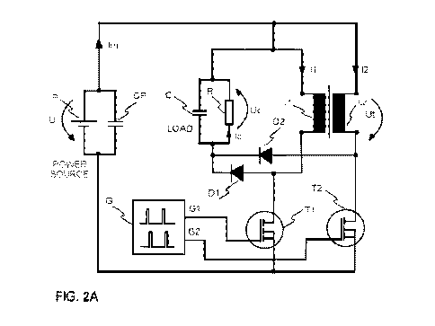
Figure 2A illustrates an exemplary switched mode converter circuit according
to
the invention. The primary circuit of the converter is similar to the prior
art circuit.
The primary circuit has an inductor winding L which is wound around a
ferromagnetic core. Capacitor CP is charged with the input voltage U of an
input
power source P. The capacitor CP is coupled to the inductor L1 with a
switching
transistor TI. The transistor is controlled to ON state with short pulses G1
of e.g.
10 ps length provided from a pulse generator G. The transistor thus connects
short current pulses from the capacitor CP to the inductor L. During the OFF
state
of the transistor T the energy of the inductor L is led through the diode
switch D1
to the load capacitor C and load R. The diode switch prevents the energy
charged
to the capacitor C from discharging to the inductor or input power source.
The ferromagnetic core has a secondary inductor winding L2. The secondary
winding is not closely wound around the core, but the winding has a larger
inner
diameter than the outer diameter of the core, thus leaving a non-ferromagnetic
space between the core and the secondary winding. The secondary winding is
connected to the load with diode D2, which allows the electrical energy to
flow
from the secondary winding to the load but not vice versa. The circuit has
another
switching transistor T2 for also switching one end of the secondary winding L2
to
the input power source. The second end of the secondary winding is connected
to
the input power source. The primary and secondary circuits are thus symmetric.
The switching transistors Ti and T2 are controlled with successive pulses,
which
first switch the transistor Ti to ON state for a short time period in first
phase. After
the primary transistor Ti has been switched back to OFF state the second
transistor T2 is switched to ON state for a short time period, such as 10...13
ps in
second phase. In the first phase the secondary winding releases electrical
energy
to the load through diode switch D2. In the second phase the secondary winding
is connected to the input voltage, increasing the release of energy from the
first
winding to the load.
Figure 4 illustrates an exemplary control sequence. G1 is the control pulse of
the
primary switch and G2 is the control signal of the secondary switch. 11 is the
current of the primary winding. At the first phase, when the primary switch is
switched ON by the G1 control signal the current of the primary winding
increases
CA 02940993 2016-08-26
WO 2015/128551 PCT/F12015/050123
12
in accordance to the input voltage and the inductance of the primary winding.
During the first phase energy flows partly to the load through the secondary
winding L2.
At the second phase the primary switch is controlled OFF by signal G1, and the
secondary switch is controlled ON by signal G2 for a short period. The
secondary
winding is thus connected to the input voltage. The current of the primary
winding
is reduced, but with a slower pace due to the effect of the voltage in the
secondary winding. While the current of the primary winding is reduced more
slowly, energy flows to the load from the primary winding for a longer time,
and
larger amount of energy flows to the load. This way, increased output power is
achieved as well as increased efficiency. The pulses G1 and G2, as well as
first
and second phases, are then repeated with an interval.
Also shown by measurements, the inventive use of secondary circuit increases
both power output of the converter as well as efficiency. In measurements of
an
exemplary circuit following values have been present:
U = Ut = 30 V
Ne = 25
Nt = 38
lin = 0,105 A
Pin = Uelin = 3,15W
Uc = 28,03 ... 28,22 V
lc = 0,104 A
Pout = Uc*Iin = 2,925 W +/- 0,01 W
q = Pout/Pin = 92,8%
The terms have following meanings:
U = input voltage
Ut = voltage of the secondary winding
Ne and Nt are the number of turns in the primary and secondary windings
respectively
lin = current supplied from the power source to the converter
Pin = power supplied from the power source to the converter
Uc = Voltage supplied by primary winding
lc = Load current
Pout = power to load
CA 02940993 2016-08-26
WO 2015/128551 PCT/F12015/050123
13
q = efficiency of the converter
As shown by the measurement, the efficiency was 92,8 %, which is essentially
higher compared to the prior art circuit of Figure 1.
The principle of function is next described by examining the above example in
more detail. In this example the ferromagnetic core is made of two U-shaped
halves which are attached into a closed magnetic circuit. The diameter of the
core
is 17 mm, and the average length of the core is 200 mm. The core has a primary
winding L1 which has Ne=25 turns. A secondary winding is located on the core,
opposite to the primary winding. The secondary winding has Nt=38 turns, and
the
diameter d2 of the secondary winding is 100 mm, and the cylindrical length of
the
winding can be e.g. 25 mm ... 35 mm. With the length of 25 mm the winding has
an inductance of L2 = 200 pH, and with the length of 35 mm its inductance is
L2 =
170 pH. In the previous example a coil of 170 pH was used, whereas in the
following example a coil of 200 pH is used. The value of dl / dt in the phase
1 is a
little lower, but they both give the same improvement in the efficiency.
In the first phase a pulse of 10 ps is fed to the primary winding, which
causes the
secondary winding to feed current to the load. In the second phase the current
of
the primary winding is fed to the load, while at the same time the secondary
winding is connected to the input voltage U. If the switches, magnetic core
and
windings would operate without losses and U = Uc, then the first and the
second
phases would be equally long, and energy taken from the voltage input by the
primary winding in the first phase would be the same as fed to the load during
the
second phase. Also the secondary winding feeds during the first phase current
to
the load as much as it takes during the second phase. In practice, the
components have losses, and the second phase is then shorter than the first.
However, as in an ideal transformer the products Ne * le and Nt * It are
almost the
same, it can be measured in the above arrangement that there is a great
difference in these products: Ne * le is remarkably bigger than Nt * It. The
measurements show that typically Ne * le = 25 * 0,9 A = 22,5 A and Nt * It =
38 *
0,45 A = 17,1 A, and then the relation of Ne * let Nt * It = 1,32, or Ne * le
= 1,32
Nt * It.
The high current difference of the primary and secondary winding effects in
the
following way: If the voltages U and Uc are equal, the secondary winding feeds
less current in the load during the phase 1, but it also takes equally less
power in
CA 02940993 2016-08-26
WO 2015/128551 PCT/F12015/050123
14
the phase 2, and no increase in the efficiency is seen. Now, if the phase 2 is
made longer in one way or the other, then the secondary winding would maintain
the higher primary current for a longer period when it decreases towards zero.
In
this case the secondary current takes power according to the formula Pt = U *
It,
but the primary current feeds power to the load according to Pe = Uc * le.
Here Nt
* It is now less than Ne * le by the multiplier 1,32. Because the winding
turns are
25 in the primary and 38 in the secondary windings and their relation is
0,658, the
voltage applied to the secondary winding in the phase two effects by this
relation
to the primary winding, but however, the secondary current is not this much
smaller, but instead 0,658 /1,32 times smaller, i.e instead 0,6 A it is 0,45 A
because of the current difference. Accordingly it takes less power in the
phase 2,
which then improves the efficiency if the phase 2 is longer than the phase 1.
There is also, however, a counter effect that starts to eliminate the
efficiency
improvement in longer periods of the phase 2. As soon as the T2 switches
voltage
to the secondary winding, the voltage in the secondary winding begins to
reduce
the current difference, and the longer the phase 2 is, the bigger the counter
effect
is in the phase 2.
In addition to the above example where Uc was smaller than U, and the phase 2
then longer than the phase 1, an improvement in the efficiency can be achieved
also when Uc is equal to or higher than U. In the latter case the phase 2
becomes
shorter than the phase 1, but also in this case the total current Nt * It in
the
secondary winding is smaller compared to Ne * le by the earlier mentioned
multiplier, which means less energy from the capacitor voltage U by the
secondary current during a short period of time, and accordingly improved
efficiency. The same effect can be achieved also by other arrangements. E.g.
if
the secondary current circuit contains a sufficient inductance itself, then
the
energy of this inductance provides a similar forward voltage for the secondary
winding as the capacitor voltage U, and the secondary current can be directed
to
the load capacitor also in the second phase with an improved efficiency. This
example is explained more in detail elsewhere in this application.
To illustrate the above effect, a practical example calculation is shown. The
voltage Uc is reduced from 30 V to 29 V (which is the sum of capacitor voltage
28,5 V and switch drop voltage 0,5 V) in order to make the phase 2 longer,
which
represents a 3,3 % decrease in the voltage Uc. This reduction increases a
little
the primary and secondary currents, but most of all, it increases the time of
the
CA 02940993 2016-08-26
WO 2015/128551 PCT/F12015/050123
phase 2 from the ideal 10 ps up to 12,5 ps depending on other settings, which
means 25% increase in the power output in the second phase.
When the relation of the number of turns of primary and secondary windings is
25
5 /38 = 0,658, the following calculation formula can be derived for the
time of the
second phase: dT2 = 0,658 * L2 * die /(Uc ¨ 0,658 * U) = 0,658 * 200 * 0,9
/(28,5
+ 0,5 ¨ 0,658 * 30) = 12,8 ps. Considering that the main factors in the
formula are
the ratio of the primary and secondary winding turns and the secondary winding
inductance, and the relatively good conformance with the measured result, this
10 calculation result supports then also the reliability of the explanation
of the effect.
It has to be noticed that many loss factors of the arrangement have not been
included in the formula, and this is why the result of calculation can be
bigger than
the measured value.
15 Figure 2B illustrates another exemplary switched mode converter circuit
according
to the invention. This embodiment is similar to the embodiment of Figure 2A,
except the inductive components of the secondary circuit. In this embodiment
the
inductance of the secondary circuit is increased with a separate inductor L3,
which is connected in series with the secondary winding L2. In this embodiment
the secondary winding L2 may have a same inductance and same inner diameter
as the primary winding L1 because the inductance of the secondary circuit is
increased with the separate inductor L3. The inductance of the secondary
circuit
is the sum of the inductances of the secondary winding L2 and the separate
inductor L3, whereby this sum inductance of the secondary circuit must be
greater
than the inductance of the primary circuit. The efficiency of this embodiment
can
be determined in a similar manner as for the embodiment of Figure 2A, but
instead of using the inductance value of the secondary winding it is necessary
to
use the sum value of the inductances of the secondary winding and the separate
inductor.
There are two thus main ways to increase the inductance of the secondary
circuit;
increasing the diameter of the secondary winding as applied in the embodiment
of
Figure 2A and using a separate series inductor as applied in the embodiment of
Figure 2B. However, it is also possible to use a combination of these two ways
to
increase the inductance of the secondary circuit, i.e. using both a secondary
winding L2 with an increased diameter and a separate series inductor.
CA 02940993 2016-08-26
WO 2015/128551 PCT/F12015/050123
16
According to an embodiment of the invention, an additional voltage source is
located at the inductance L3 location in the component topology. According to
an
ensemble of embodiments the voltage source can comprise at least one of the
group comprising: Inductor L3, capacitor C3, accumulator A3. The dashed lines
illustrate optionality between the combinations in the embodiments. According
to a
further embodiment the additional voltage source indicated in the Fig 2B can
be
embodied similarly also in Fig 2C as indicated in Fig 2B and the accompanying
text. Based on the illustrated embodiments, although an embodiment example
with parallel coupled multi-component comprising group is shown, a skilled
person in the art can provide other topologies of these components (L3, 03,
A3)
comprising in series coupled components. In addition resistive components can
be used additionally to fit the reactance to the coupling for the indicated
location.
Figure 20 illustrates a circuit diagram of a further exemplary switched mode
power converter. This embodiment is similar to the embodiment of Figure 2A,
except that the secondary winding is not connected to the power source with a
controllable switch. Instead, the secondary winding is only connected to the
load
through the diode D2. An increase in efficiency is not quite as high as in the
embodiment of Figure 2A, but this circuit has fewer components and may be
useful in some power supply applications. According to an embodiment of the
invention an additional voltage source comprising at least one of the group
comprising an inductance L3, capacitor 03 and an accumulator A3 can be added
into the embodied circuit as an alternative to the secondary switch T2 or
supplementary. Potential locations for such additional voltage sources are
illustrated via the exemplified alternatives for single additional voltage
sources, or
combinations thereof. Alternative character of a couplings in Figure 20 is
indicated by a dashed line. Although same symbols used for alternative
components in different locations, the example does not limit the component
values only to the same value.
Fig. 3 illustrates a circuit diagram of a further exemplary switched mode
power
converter in accordance with the present invention. In this embodiment one of
the
two terminals of the load is coupled to the same fixed polarity as the
controllable
switches Ti and T2. In the embodiments of Figures 2A and 2B the load terminal
is
coupled to the same fixed potential as the windings L1 and L2. In the
embodiment
of Figure 3 the input voltage U is added to the voltages of the windings L1
and L2
when energy is transferred to the load. Therefore, energy is also transferred
to the
load from the input source during the both phases 1 and 2 of the converter:
CA 02940993 2016-08-26
WO 2015/128551 PCT/F12015/050123
17
- In phase 1 the load voltage -Uc = -57 V and the input voltage U = 30 V both
affect in the secondary winding. The difference of these voltages is 27 V, and
now the effective counter voltage in this example is -27 V, which is about the
same as in the previous example, i.e. - Uc = - 29 V. In phase 1 the primary
.. winding is connected to the input voltage U = 30 V, which causes a voltage
in the
secondary winding, and makes the currents rise in the secondary winding
according to the secondary voltage, -Uc and inductances in the secondary
winding, and in the primary winding in a similar way as in the previous
examples;
- In phase 2 both input voltage U and the load voltage ¨Uc affect in the
primary
.. winding. The counter voltage is -27 V in this example, whereby considering
the
reduced forward voltages from the secondary circuit to the primary circuit the
counter voltage is lower by 2 V compared to the earlier example where it was
29
V. In this situation the given equation gives a longer time period for phase 2
of the
converter;
- The calculatory time length for phase 2 can be derived by using the given
formula dt = (Ne/Nt) * L2 * die / (Uc ¨ (Ne/Nt) * U). In the present
embodiment
other values in the formula are the same as in the embodiment of Figure 2A
except voltage Uc, which now has the value Uc = U-56,5 V ¨ 0,5 V = 27 V. The
formula now gives dt = 16,3 ps, which matches with measurements.
In an embodiment of the invention the smaller magnetic flux at the location of
the
secondary winding induces a smaller counter voltage in the secondary winding
during the second phase, which requires then less input power by the secondary
winding in the second phase during the reduction of the primary and secondary
currents.
The output power of the converter is thus increased when compared to the
embodiment of Figure 2A, and the efficiency is also increased by 3-4
percentage
units.
Figure 4 illustrates a diagram of an exemplary control sequence for circuits
of
Figures 2 and 3. Although the examples on rise and discharge of current 11, in
respect to the pulses G1 and G2 having the state ON as indicated, illustrated
in
the embodiments in Fig 4, as well as the intermediate time between two
successive rises of same phase, the embodiments are not limited only to the
shown example. In practice the component values in combination to the pulse
generator's G pulses determine the duration of the rise and discharge, as well
as
CA 02940993 2016-08-26
WO 2015/128551 PCT/F12015/050123
18
the intermediate time between the triangular pulses of 11 embodied in in
Fig.4, i.e.
details of the pulse geometry of 11.
Figure 5 illustrates an exemplary ferromagnetic core F according to the
invention,
which has a primary winding L1 and a secondary winding L2. The inner diameter
d2 of the secondary winding L2 is greater than the inner diameter dl of the
primary winding.
In this patent specification the structure of the other various components of
a
switched-mode power converter is not described in more detail as they can be
implemented using the description above and the general knowledge of a person
skilled in the art. Each of the elements such as the switching transistors,
the core,
the windings, and the separate inductor, can include one component or it may
consist of two or several components. The component types have been
mentioned as examples, and a person skilled can think of several alternative
component types providing the functionalities described above.
The switching element Ti and T2 of the converter circuit may be a power
semiconductor, such as MOSFET or an IGBT, for example. The gates of the
.. switching transistors are controlled with corresponding outputs of a pulse
generator G.
Figure 6A illustrates a method for converting electrical power, wherein an
electrical power converter of switching type is used for the method
implementation. In an embodiment of the method, T1 is controlled 601 to open
by
the corresponding level of the pulses of GI . Energy is stored 602 to L1, L2
and
load. Ti is controlled 603 to close by the corresponding GI phase, and
simultaneously T2 by G2 to open in those embodiments that use T2. Energy is
released 604 from L1 and L2, energy is added from U to L2. Next, T2 is
controlled
.. 605 to close by G2 in those embodiments that use T2. The cycle starts again
from
the 601, as illustrated by the arrows. At a first phase of the method a first
primary
switch Ti of the converting circuit is controlled by pulses of a pulse
generator so
that the first primary switch Ti connects according to the pulses of GI of
input
voltage U to a primary winding L1 of a ferromagnetic core F. The pulse
generator
G is configured and/or coupled to produce pulses that correspond the ON state
of
the Ti, and between two immediate such pulses there is a pulse level, called
here
as pitch, corresponding the OFF state of the Ti. Energy is stored to L1, L2
and
load.
CA 02940993 2016-08-26
WO 2015/128551 PCT/F12015/050123
19
Ti is controlled by G1 close and T2 simultaneously open by G2. According to an
embodiment, in a second phase energy is released thereafter, from the primary
winding L1, the energy being led to a load through second switch T2, whereby
the
.. current 11 of the primary winding L1 is decreased. According to an
embodiment of
the invention this energy is transferred to the primary winding L1 during said
decrease of current 11 of the primary winding L1 to the primary winding and/or
another energy source in order to improve the efficiency of the conversion
energy
of the secondary winding L2.
According to an embodiment in alternative or supplementary, during the second
phase controlling the secondary switch T2 is to connect according to the pulse
of
G2 the input voltage U to a secondary winding L2 of the ferromagnetic core F
in
order to increase the release of energy from the primary winding L1 to the
load
.. LOAD, C, R, so as leading during the first phase released energy from the
secondary winding L2 of the core F to the load through second secondary switch
T2. T2 is controlled to close, before the T1 being controlled to open 601 in
next
cycle. In those embodiments that use other energy directing component than T2,
the circuit operation follows the embodiments illustrated in Fig 2C, and the
energy
is directed to the load according to the embodied circuit topology.
According to an embodiment variant, the pitch is set to a constant duration,
but
according to an embodiment variant it is made adjustable. According to an
embodiment of the invention the ON state duration is set to a constant
duration,
but according to an embodiment variant of the invention it is made adjustable.
According to an embodiment of the invention duration of a pulse and/or a pitch
is
determined by the pulse generator's pulse geometry, but in a variant of such
an
embodiment by an intermediate latch-circuit adjusted for pulse geometry and
its
details in respect of amplitude, pitch and/or pulse length.
According to an embodiment of the invention the pulse generator can be
adjusted
to change from a first pulse duration to another pulse duration. According to
an
embodiment of the invention the pulse generator can be used in adjusting to
change from a first pitch duration to a second pitch duration.
According to an embodiment of the invention the pulses of G2 can be same way
adjusted as disclosed above for the G1. According to an embodiment the G1 is
made adjustable independently on G2. In alternative or supplementary,
according
CA 02940993 2016-08-26
WO 2015/128551 PCT/F12015/050123
to an embodiment the G2 is made adjustable independently on G1. According to
an embodiment of the invention at least on pitch or pulse duration of at least
one
of G1 and G2 adjustment is step-wise, but according to an embodiment of the
invention the adjustment is gliding. This way the pulse characteristics of G1
can
5 be changed from a first set of pulsing parameters to a second set of
pulsing
parameters, so facilitating use of the converter for a different type of
loads.
According to the step-wise change the switching between different type of
loads
can be made instantly as fast as the response times of the electronics allow.
10 Although in embodiments of the invention the pulses of G1 and/or G2 as
such are
considered to be generated as square pulses as illustrated in the example of
Figure 4, i.e. pulses with sharp rise and fall time with essentially constant
value
level there between, so as considered in terms of analogue square pulse
geometry, according to an embodiment of the invention the pulse generator G or
15 .. an interfacing latch circuit driving the Ti and/or T2 in G's conduction
(the latch
may be included into G in embodiment variant) can be adjusted digitally to
generate pulses G1 and/or G2. In some embodiment variants at least one of the
Ti and T2 can be driven directly by a digital signal or two forming suitable
pulse
trains for the respective G1 and G2 to be combined as illustrated in Figure 4.
This
20 ways the load can be energized in accordance of the digital control
signal.
Figure 6B illustrates a variant of an embodiment embodied as a method of
converting electrical power, with a switched mode converter according to an
embodiment of the invention. Such a converter is coupled for converting
electrical
power via utilization of an unequal magnetic flux in the core F, the coupling
having
at least one of said primary and secondary windings L1, L2 being located,
and/or
has such a shape or a diameter dl, d2, at some distance from the secondary and
primary winding L2, L1, respectively, to provide an unequal magnetic flux.
According to an embodiment of the invention the method comprises: controlling
611 in the first phase, the first controllable switch Ti with primary control
pulses
G1 to energize the primary winding L1 to increase its current 11 to create a
magnetic flux in the core F. The method comprises switching 612 by said
primary
control pulses G1 the first controllable primary switch G1 into ON state to
connect
the primary winding L1 to input power during said control pulse G1. The method
comprises also energizing 613 in the second phase directly after the primary
pulses G1 each the secondary winding L2 by secondary pulses G2 of input power
P via the second primary switch T2 in ON state during said secondary pulses
G2.
CA 02940993 2016-08-26
WO 2015/128551 PCT/F12015/050123
21
In the embodiment of the method, it comprises also directing 614 by setting
said
first controllable primary switch Ti into OFF state, the primary winding L1 to
release magnetic energy of the magnetic flux to the load LOAD, R, C, between
the
ON states of the primary pulses G1, whereby the current 11 of the primary
winding
L1 decreases. The period of G2 in ON state of T2 can be embodied according to
the embodiments illustrated as associated to Figure 4. The next cycle is
scheduled 615 to begin when Ti is controlled to open as in phase 611.
The control functions of the switched-mode converter can be implemented with
analogue circuits, such as an ASIC circuit, whereby a simple implementation
would be achieved. However, to achieve a more advanced functionality, a
digital
implementation is preferred. When a microcontroller/processor is used the
circuit
requires a suitable processor program, which is executed in a device. To
convert
a known device or system into equipment according to the invention it is
necessary, in addition to the hardware modifications, to store into the memory
means a set of machine-readable instructions that instruct the
microprocessor(s)
to perform the functions described above. Composing and storing into memory of
such instructions involves known technology which, when combined with the
teachings of this patent application, is within the capabilities of a person
skilled in
the art.
Above, only some embodiments of the solution according to the invention have
been described. The principle according to the invention can naturally be
modified
within the frame of the scope defined by the claims, for example, by
modification
.. of the details of the implementation and ranges of use.
The present invention can be applied in external and internal DC power
supplies
for various purposes and for various electronic devices