Note: Descriptions are shown in the official language in which they were submitted.
CA 02942999 2016-09-16
NON-POLAR BLUE LED EPITAXIAL WAFER BASED ON LAO
SUBSTRATE AND PREPARATION METHOD THEREOF
Field of the Invention
The present invention relates to an LED epitaxial wafer and a preparation
method
thereof, and in particular, to a non-polar blue light LED epitaxial wafer
based on an
LAO substrate and a preparation method thereof.
Background of the Invention
At present, substrates of LED blue light epitaxial wafers are mainly sapphire.
The
LED technology based on a sapphire substrate has two serious problems.
Firstly, the
mismatch rate of the sapphire and a GaN crystal lattice is as high as 17%.
Such high
lattice mismatch results in a high defect density of the sapphire based LED
epitaxial
wafer, thereby greatly influencing the luminous efficiency of an LED chip.
Secondly,
the price of the sapphire substrate is very high, resulting in very high
production cost
of a nitride LED.
Another major reason for the low luminous efficiency of the LED chip is that
the
current GaN based LEDs in wide use have polarity. At present, the most ideal
material
for manufacturing of a high efficient LED device is GaN. The GaN is of a
closely
packed hexagonal crystal structure, whose crystal faces are divided into a
polar face,
which is a c face [(0001) face] and non-polar faces, which include an a face
[(11-20)
face] and an m face [(1-100) face]. Currently, most GaN based LEDs are
constructed
based on the polar face of the GaN. On the polar face of the GaN, the centroid
of the
Ga atom cluster does not coincide with the centroid of the N atom cluster,
thus
forming an electric dipole and generating a spontaneous polarization field and
a
piezoelectric polarization field, and further, causing a Quantum-confined
Stark effect
(QCSE). The QCSE causes electrons being separated from holes, and reduces the
radiation recombination efficiency of charge carriers, which in turn
influences the
luminous efficiency of LED, and causes instability of a light emitting
wavelength of
the LED.
1
CA 02942999 2016-09-16
Summary of the Invention
The technical problem to be solved by the present invention is to provide a
non-polar
blue light LED epitaxial wafer based on an LAO substrate and a preparation
method
thereof. The non-polar blue light LED epitaxial wafer has the advantages of
low
defect density, good crystalline quality and good luminous performance, and
having
low preparation cost.
The technical solution used for solving the above technical problem of the
present
invention is to provide a non-polar blue light LED epitaxial wafer based on an
LAO
substrate, including the substrate. The substrate is the LAO substrate, and a
buffer
layer, a first non-doped layer, a first doped layer, a quantum well layer, an
electron
barrier layer and a second doped layer are sequentially arranged on the LAO
substrate.
According to the non-polar blue light LED epitaxial wafer based on the LAO
substrate, the buffer layer is a non-polar m face GaN buffer layer, the first
non-doped
layer is a non-polar non-doped u-GaN layer, the first doped layer is a non-
polar n-type
doped GaN film, the quantum well layer is a non-polar InGaN/GaN quantum well
layer, the electron barrier layer is a non-polar m face AlGaN electron barrier
layer, and
the second doped layer is a non-polar p-type doped GaN film.
To solve the above technical problem, the present invention provides a
preparation
method of a non-polar blue light LED epitaxial wafer based on an LAO
substrate,
including the following steps: a) adopting the LAO substrate, selecting the
crystal
orientation, and cleaning the surface of the LAO substrate; b) annealing the
LAO
substrate, and forming an AIN seed crystal layer on the surface of the LAO
substrate;
and c) sequentially forming a non-polar m face GaN buffer layer, a non-polar
non-doped u-GaN layer, a non-polar n-type doped GaN film, a non-polar
InGaN/GaN
quantum well, a non-polar m face AlGaN electron barrier layer and a non-polar
p-type
doped GaN film on the LAO substrate by adopting metal organic chemical vapor
deposition.
According to the above preparation method of the non-polar blue light LED
epitaxial
2
CA 02942999 2016-09-16
wafer based on the LAO substrate, wherein the step b) includes the following
processes: baking the LAO substrate at high temperature of 900-1200 C for 1-4
h
followed by cooling to the room temperature in air, then passing N2 plasma to
keep
the temperature for 30-80 minutes, and forming the MN seed crystal layer on
the
surface of the LAO substrate by radio frequency plasma enhanced metal organic
chemical vapor deposition, wherein the flow of the N plasma is 40-90 sccm, and
the
radio frequency power for generating the plasma nitrogen is 200-500W.
According to the above preparation method of the non-polar blue light LED
epitaxial
wafer based on the LAO substrate, wherein in the step c), the process of
forming the
non-polar m face GaN buffer layer is as follows: cooling the LAO substrate to
400-800 C, passing TMGa and the N plasma, and controlling the pressure of a
reaction chamber within the range of 400-700 ton, the flow of the N plasma
within
the range of 40-90 sccm, the radio frequency power of generating the plasma
nitrogen
within the range of 200-700W, and the V/III ratio within the range of 800-
1200.
According to the above preparation method of the non-polar blue light LED
epitaxial
wafer based on the LAO substrate, wherein in the step c), the process of
forming the
non-polar non-doped u-GaN layer is as follows: controlling the temperature of
the
LAO substrate with the range of 1000-1500 C, passing the TMGa, controlling the
pressure of the reaction chamber at 400 torr and the V/III ratio at 180.
According to the above preparation method of the non-polar blue light LED
epitaxial
wafer based on the LAO substrate, wherein in the step c), the process of
forming the
non-polar n-type doped GaN film is as follows: controlling the temperature of
the
LAO substrate within the range of 1000-1300 C, passing the TMGa and SiH4,
maintaining the flow of the SiH4 within the range of 60-100 sccm, and
controlling the
pressure of the reaction chamber at 240 ton, the V/III ratio at 160, and the
dopped
electron concentration within the range of 1.0x10¹⁷ to 5.3x1019cm-3.
According to the above preparation method of the non-polar blue light LED
epitaxial
wafer based on the LAO substrate, wherein in the step c), the process of
forming the
non-polar InGaN/GaN quantum well is as follows:
forming a barrier layer: controlling the temperature of the LAO substrate
within the
3
CA 02942999 2016-09-16
range of 750-950 C, closing H2, passing the TEGa and ammonia gas, and
controlling
the pressure of the reaction chamber at 200 torr, the V/III ratio at 986, and
the
thickness within the range of 10-15nm; and
forming a well layer: controlling the temperature of the LAO substrate within
the
range of 750-950 C, closing H2, passing the TEGa, TMIn and the ammonia gas,
and
controlling the pressure of the reaction chamber at 200 torr, the V/III ratio
at 1439,
and the thickness within the range of 2-4nm.
According to the above preparation method of the non-polar blue light LED
epitaxial
wafer based on the LAO substrate, wherein in the step c), the process of
forming the
non-polar m face AlGaN electron barrier layer is as follows: rising the
temperature of
the LAO substrate to 900-1050 C, passing the TMGa and the ammonia gas, and
controlling the pressure of the reaction chamber at 200 torr and the V/III
ratio at 986.
According to the above preparation method of the non-polar blue light LED
epitaxial
wafer based on the LAO substrate, wherein in the step c), the process of
forming the
non-polar p-type doped GaN film is as follows: controlling the temperature of
the
LAO substrate within the range of 900-1100 C, passing the TMGa, CP2Mg and the
ammonia gas, maintaining the flow of the CP2Mg at 250-450 sccm, and
controlling
the pressure of the reaction chamber at 200 torr, the V/III ratio within the
range of
1000-1250, and the hole doping concentration within the range of 1.0x10¹⁶ to
2.2x10 1 8CM-3.
Compared with the prior art, the present invention has the following
beneficial effects
that: according to the non-polar blue light LED epitaxial wafer based on the
LAO
substrate and the preparation method thereof provided by the present
invention, the
LAO substrate is adopted, and the buffer layer, the first non-doped layer, the
first
doped layer, the quantum well layer, the electron barrier layer and the second
doped
layer are arranged on the LAO substrate in sequence, so that the non-polar
blue light
LED epitaxial wafer has the advantages of low defect density, good crystalline
quality
and good luminous performance, and have low preparation cost.
4
CA 02942999 2016-09-16
Brief Description of the Drawings
Fig.1 is a schematic diagram of a structure of a non-polar blue light LED
epitaxial
wafer based on an LAO substrate of the present invention;
Fig.2 is a schematic diagram of a structure of a preparation device for a non-
polar
blue light LED epitaxial wafer based on an LAO substrate of the present
invention;
Fig.3 is a schematic flow chart of a preparation of a non-polar blue light LED
epitaxial wafer based an LAO substrate of the present invention;
Fig.4 is an XRD test diagram of a non-polar blue light LED epitaxial wafer
grown on
a (001) face of an LAO substrate of the present invention;
Fig.5 is a PL spectrum test diagram of a non-polar m face blue light LED
epitaxial
wafer grown on an LAO substrate of the present invention at the room
temperature;
Fig.6 is an EL spectrum test diagram of a non-polar m face blue light LED
epitaxial
wafer grown on an LAO substrate of the present invention at the room
temperature.
Detailed Description of the Embodiments
The present invention will be further described below in combination with
accompany
drawings and embodiments.
Fig.1 is a schematic diagram of a structure of a non-polar blue light LED
epitaxial
wafer based on an LAO substrate of the present invention.
Please refer to Fig. 1 . The non-polar blue light LED epitaxial wafer based on
the LAO
substrate provided by the present invention includes a substrate. The
substrate is the
LAO substrate, and a buffer layer, a first non-doped layer, a first doped
layer, a
quantum well layer, an electron barrier layer and a second doped layer are
arranged on
the LAO substrate in sequence. According to the non-polar blue light LED
epitaxial
wafer grown on the LAO substrate provided by the present invention, the LAO
substrate is also called a lanthanum aluminum oxide substrate which is
composed of
La, Al and 0 elements, and the molecular formula is LaAlx0y. As shown in
Fig.!, the
non-polar blue light LED epitaxial wafer provided by the present invention
includes
an LAO substrate 10, a non-polar m face GaN buffer layer 11, a non-polar non-
doped
u-GaN layer 12, a non-polar n-type doped GaN film 13, a non-polar InGaN/GaN
5
CA 02942999 2016-09-16
quantum well layer 14, a non-polar m face AlGaN electron barrier layer 15 and
a
non-polar p-type doped GaN film 16, which are arranged from bottom to top in
sequence.
Fig.2 is a schematic diagram of a structure of a preparation device for a non-
polar
blue light LED epitaxial wafer based on an LAO substrate of the present
invention.
Please refer to Fig.2. 20 and 21 respectively represent NH3 and SiH4, which
are used
for providing N and Si; 22 represents H2, which is used as a carrier gas and
for
conveying Cp2Mg, TMGa and TMIn; 23, 24 and 25 respectively represent the
Cp2Mg,
the TMGa and the TMIn, which are used for providing Mg, Ga and In necessary
for
the growth of LED; 26 represents is a mechanical arm, which is used for
conveying
the substrate and a sample; 27 represents a radio frequency induction heater,
which is
used for heating and controlling the temperature of the substrate; 28
represents a
graphite plate, which is used for bearing the LAO substrate; 29 represents a
reaction
chamber, which is used for generating chemical reactions on various reactant
gases to
generate the LED; 30 represents a spray head, which is a device used for
uniformly
jetting the fully mixed reactant gases onto the surface of the substrate; 31
represents a
radio frequency plasma source device, which is used for providing active N;
and
32-40 represent valves, which are used for controlling the gas conveyance
states of
various pipelines. MFC represents a flow controller, which is used for
controlling the
gas flow to meet the growth demands.
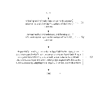
Fig.3 is a schematic flow chart of a preparation of a non-polar blue light LED
epitaxial wafer based an LAO substrate of the present invention.
Please refer to Fig.3. the preparation method of the non-polar blue light LED
epitaxial
wafer grown on the LAO substrate of the present invention specifically
includes the
following steps:
step Sl: adopting the LAO substrate, selecting the crystal orientation, and
cleaning the
surface of the LAO substrate;
step S2: annealing the LAO substrate, and forming an AIN seed crystal layer on
the
surface of the LAO substrate; and
step S3: sequentially forming a non-polar m face GaN buffer layer, a non-polar
6
CA 02942999 2016-09-16
non-doped u-GaN layer, a non-polar n-type doped GaN film, a non-polar
InGaN/GaN
quantum well, a non-polar m face AlGaN electron barrier layer and a non-polar
p-type
doped GaN film on the LAO substrate by metal organic chemical vapor
deposition.
A specific embodiment is provided below with the preparation steps and process
conditions as follows:
(1) adopting an LAO substrate, and selecting the crystal orientation;
(2) cleaning the surface of the substrate;
(3) annealing the substrate: baking the substrate at high temperature of 900-
1200 C
for 1-4 h followed by cooling the substrate to the room temperature in air,
then
passing N2 plasma to keep the temperature for 30-80 minutes, and forming an
AIN
seed crystal layer on the surface of the substrate to provide a template for
the growth
of a GaN film, wherein the flow of the N plasma is 40-90 sccm, and the radio
frequency power for generating the plasma nitrogen is 200-500W;
(4) growing a non-polar m face GaN buffer layer by radio frequency (RF) plasma
enhanced metal organic chemical vapor deposition (MOCVD), wherein the process
conditions are as follows: the substrate is cooled to 400-800 C, the TMGa and
the N
plasma are passed, the pressure of a reaction chamber is 400-700 ton, the flow
of the
N plasma is 40-90 sccm, the radio frequency power of generating the plasma
nitrogen
is 200-700W, and the V/III ratio is 800-1200;
(5) growing a non-polar non-doped u-GaN layer by the MOCVD process, wherein
the
process conditions are as follows: the temperature of the substrate is 1000-
1500 C,
the TMGa is passed, the pressure of the reaction chamber is 400 ton, and the
V/III
ratio is 180;
(6) growing a non-polar n-type doped GaN film by the MOCVD process, wherein
the
process conditions are as follows: the temperature of the substrate is 1000-
1300 C,
the TMGa and SiH4 are passed, the flow of the SiH4 is maintained at 60-100
sccm,
the pressure of the reaction chamber is 200 ton, the V/III ratio is 160, and
the doped
electron concentration is 1.0x10¹⁷ to 5.3x1019cm-3;
(7) growing a non-polar InGaN/GaN quantum well by the MOCVD process, wherein
the process conditions for forming a barrier layer are as follows: , the
temperature of
7
CA 02942999 2016-09-16
the LAO substrate is 750-950 C, H2 is closed, the TEGa and ammonia gas are
passed,
the pressure of the reaction chamber is 200 torr, the V/III ratio is 986, and
the
thickness is 10-15nm; and wherein the process conditions for forming a well
layer are
as follows: the temperature of the LAO substrate is 750-950 C, H2 is closed,
the
TEGa, TMIn and the ammonia gas are passed, the pressure of the reaction
chamber is
200 torr, the V/III ratio is 1439, and the thickness is 2-4nm;
(8) growing a non-polar m face AlGaN electron barrier layer by the MOCVD
process,
wherein the process conditions are as follows: the temperature of the LAO
substrate is
raised to 900-1050 C, the TMGa and the ammonia gas are passed, the pressure of
the
reaction chamber is 200 ton-, and the V/III ratio is 986; and
(9) growing a non-polar p-type doped GaN film by the MOCVD process, wherein
the
process conditions are as follows: the temperature of the LAO substrate is
900-1100 C, the TMGa, CP2Mg and the ammonia gas are passed, the flow of the
CP2Mg is maintained at 250-450 sccm, the pressure of the reaction chamber is
200
torr, the V/III ratio is 1000-1250, and the doped hole concentration is
1.0x10¹⁶ to
-
2.2x 101 8 cm -3
Fig.4 is an XRD test diagram of a non-polar blue light LED epitaxial wafer
grown on
a (001) face of an LAO substrate of the present invention.
Fig.4 shows a full width at half maximum (FWHM) value of a X ray rocking curve
of
the LED epitaxial wafer as tested in the present invention. The full width at
half
maximum (FWHM) value is less than 0.1 degree, which indicates that the non-
polar
blue light LED epitaxial wafer prepared in the present invention has very good
performance no matter on defect density or on crystalline quality.
Fig.5 is a PL spectrum test diagram of a non-polar m face blue light LED
epitaxial
wafer grown on an LAO substrate of the present invention at the room
temperature.
Fig.5 shows a emission peak having a wavelength of 460nm, and the full width
at half
maximum of 23nm, as tested by a PL spectrum at a temperature of 293K in the
present invention. This indicates that the non-polar GaN film prepared in the
present
invention has very good performance on optical properties.
Fig.6 is an EL spectrum test diagram of a non-polar m face blue light LED
epitaxial
8
CA 02942999 2016-09-16
wafer grown on an LAO substrate of the present invention at the room
temperature.
Fig.6 shows a emission peak having a wavelength of 461m, the full width at
half
maximum of 22nm and the output power of 7.8mw@20mA, as tested by an EL
spectrum at the temperature of 293K in the present invention. This indicates
that the
non-polar GaN film prepared in the present invention has very good performance
on
electrical properties.
In summary, the present invention provides a non-polar blue light LED
epitaxial wafer
based on the LAO substrate and the preparation method thereof. The LAO
substrate is
adopted, and the non-polar m face GaN buffer layer, the non-polar non-doped u-
GaN
layer, the non-polar n-type doped GaN film, the non-polar InGaN/GaN quantum
well,
the non-polar m face AlGaN electron barrier layer and the non-polar p-type
doped
GaN film are arranged on the LAO substrate in sequence. Compared with the
prior art,
the present invention has the advantages of simple growth process and low
preparation cost, and the non-polar blue light LED epitaxial wafer prepared
has the
advantages of low defect density, good crystalline quality and good electrical
and
optical performances.
Although the present invention has been disclosed above by the preferred
embodiments, the present invention is not limited hereto, any skilled in the
art can
made some modifications and perfections without departing from the spirit or
scope
of the present invention which are covered and by the appended claims.
9