Note: Descriptions are shown in the official language in which they were submitted.
CA 02944526 2016-09-30
WO 2015/149324 PCT/CN2014/074715
CAPACITIVE TOUCH SENSOR
TECHNICAL FIELD
The embodiments described below relate to touch sensors and, more
particularly,
to capacitive touch sensors.
BACKGROUND
Instruments are used in industrial applications to control processes. For
example,
flow metersare used to measure the mass flow rate, density, and other
characteristics of
materials flowing through a pipeline. The flowing materials can comprise
liquids, gases,
combined liquids and gases, solids suspended in liquids, liquids including
gases and
suspended solids, etc. The flow meter can be used to measure a flow rate
(i.e., by
measuring a mass flow through the flow meter), and can further be used to
determine
the relative proportions of components in a flow stream. The flow meter can
provide
data of the measurements through, for example, an interface that is accessible
by an
operator. Using the data provided by the flow meter, other instruments such as
valves
and pumps can control the materials flowing through the pipeline.
The flow metercan be employed in a wide range of industrial applications. As a
result, the flow meter is often required to meet a wide range of environmental
specifications. For example, the flow meter may be required to reliably
function in high
humidity while being subjected to temperature cycles or corrosive
environments. The
flow meter might also be required to accept data input in these environments.
That is, an
operator working on the pipeline may be required to input data into the flow
meter under
various environmental conditions. To input the data, the operator typically
presses
buttons onan interface. Due to the environmental conditions, the buttons in
prior art
interfaces can be prone to performance issues. For example, mechanical buttons
can be
subjected to corrosion in high humidity environments. Infrared buttons might
need
calibration routines to operate reliably in both high and low temperature. As
a result, the
data input through prior art buttons can include errors.
Although the interface could be configured for specific environments, such
special configurations are cost prohibitive and can be the source of
additional defects.
Accordingly, there is a need for touch sensors that reliably operate in a wide
range of
environmental conditions.
1
CA 02944526 2016-09-30
WO 2015/149324 PCT/CN2014/074715
SUMMARY
A capacitive touch sensor (100) is provided. According to an embodiment, the
capacitive touch sensor (100) comprises an electrode (110) disposed between a
plate
(120) and a spring (130) wherein the spring (130) presses the electrode (110)
towards
the plate (120) in a direction that is substantially parallel to a
longitudinal length of the
spring (130) and the electrode (110) has a flat sensing surface (112) parallel
with the
plate (120).
A method of forming a capacitive touch sensor (100) is provided. According to
an embodiment, the method comprises forming a plate (120), forming a spring
(130)
having a longitudinal length (L), and forming and disposing an electrode (110)
between
the plate (120) and the spring (130) wherein the spring (130) presses the
electrode (110)
towards the plate (120) in a direction that is substantially parallel to the
longitudinal
length (L) of the spring (130) and the electrode (110) has a flat sensing
surface (112)
parallel with the plate (120).
An interface (10) having a capacitive touch sensor (100) is provided.
According
to an embodiment, the interface (10) comprises an operation module (12), a
display
cover (14), a transmitter (16) wherein the display cover (14) is coupled to
the transmitter
(16) and the operation module (12) is disposed between the display cover (14)
and the
transmitter (16). The interface (10) further comprises the capacitive touch
sensor (100)
comprising an electrode (110) pressed against a plate (120) coupled to the
display cover
(14).
ASPECTS
According to an aspect, a capacitive touch sensor (100), comprises an
electrode
(110) disposed between a plate (120) and a spring (130) wherein the spring
(130)
presses the electrode (110) towards the plate (120) in a direction that is
substantially
parallel to a longitudinal length (L) of the spring (130) and the electrode
(110) has a flat
sensing surface (112) parallel with the plate (120).
Preferably, the capacitive touch sensor (100), wherein the electrode (110)
further
comprises an extending portion (114) that extends away from the sensing
surface (112).
2
CA 02944526 2016-09-30
WO 2015/149324 PCT/CN2014/074715
Preferably, the capacitive touch sensor (100), wherein the extending portion
(114)
interfaces with a panel (150)that prevents a movement of the electrode (110)
relative to
the plate (120).
Preferably, the capacitive touch sensor (100), wherein the extending portion
(114)
interfaces with the spring (130) to prevent a movement of the electrode (110)
relative to
the spring (130).
Preferably, the capacitive touch sensor (100), wherein the spring (130)
comprises
a first distal portion (134) that presses the electrode (110) towards the
plate (120) and a
second distal portion (132) that is coupled to a circuit board (140).
Preferably, the capacitive touch sensor (100), wherein the first distal
portion (134)
is comprised of an inverse cone region that presses against the electrode
(110).
Preferably, the capacitive touch sensor (100), wherein the spring (130)
comprises
a conductor that electrically couples the electrode (110) with the circuit
board (140).
Preferably, the capacitive touch sensor (100), wherein the spring (130) holds
the
electrode (110) spaced apart from the circuit board (140).
Preferably, the capacitive touch sensor (100), wherein the spring (130) is a
coil
spring with the longitudinal length (L).
According to an aspect, a method of forming a capacitive touch sensor (100)
comprises forming a plate (120), forming a spring (130) having a longitudinal
length (L),
and forming and disposing an electrode (110) between the plate (120) and the
spring
(130) wherein the spring (130) presses the electrode (110) towards the plate
(120) in a
direction that is substantially parallel to the longitudinal length (L) of the
spring (130)
and the electrode (110) has a flat sensing surface (112) parallel with the
plate (120).
Preferably, the electrode (110) further comprises an extending portion (114)
that
extends away from the sensing surface (112).
Preferably, the extending portion (114) interfaces with a panel (150)that
prevents
a movement of the electrode (110) relative to the plate (120).
Preferably, the extending portion (114) interfaces with the spring (130) to
prevent movement of the electrode (110) relative to the spring (130).
Preferably, the spring (130) comprises a first distal portion (134) that
presses the
electrode (110) towards the plate (120) and a second distal portion (132) that
is coupled
to a circuit board (140).
3
CA 02944526 2016-09-30
WO 2015/149324 PCT/CN2014/074715
Preferably, the first distal portion (134) is comprised of an inverse cone
region
that presses against the electrode (110).
Preferably, the spring (130) comprises a conductor that electrically couples
the
electrode (110) with the circuit board (140).
Preferably, the spring (130) holds the electrode (110) spaced apart from the
circuit board (140).
Preferably, the spring (130) is a coil spring with the longitudinal length
(L).
According to an aspect, an interface (10) having a capacitive touch sensor
(100)
comprises an operation module (12), a display cover (14), a transmitter (16)
wherein the
display cover (14) is coupled to the transmitter (16) and the operation module
(12) is
disposed between the display cover (14) and the transmitter (16), and the
capacitive
touch sensor (100) comprising an electrode (110) pressed against a plate (120)
coupled
to the display cover (14).
Preferably, the interface (10) further comprises a spring (130) wherein the
electrode (110) is pressed against the plate (120) by the spring (130).
Preferably, the interface (10) wherein the spring (130) extends from a circuit
board (140) disposed between the operation module (12) and the transmitter
(16).
Preferably, the interface (10) wherein the electrode (110) is pressed against
the
plate (120) by the spring (130) in a direction that is substantially parallel
to a
longitudinal length (L) of the spring (130).
Preferably, the interface (10) wherein the electrode (110) is coupled to a
panel
(150)that is coupled to the operation module (12).
BRIEF DESCRIPTION OF THE DRAWINGS
The same reference number represents the same element on all drawings. It
should be understood that the drawings are not necessarily to scale.
FIG. 1 shows a front plan view of an interface 10 with capacitive touch
sensors
100 according to an embodiment.
FIG. 2 shows an exploded perspective view of the interface 10 with the
capacitive touch sensors 100.
FIG. 3 shows a further exploded perspective view of the interface 10 with the
capacitive touch sensors 100.
4
CA 02944526 2016-09-30
WO 2015/149324 PCT/CN2014/074715
FIG. 4 shows an exploded perspective view of a simplified model of the
capacitive touch sensor 100 for clarity.
FIGS. 5a and 5b show an enlarged perspective view of the electrode 110 and an
enlarged side view of the spring 130, respectively.
FIG. 6 shows a cross sectional side view of the capacitive touch sensor 100
taken
at 6-6 in FIG. 4.
FIG. 7 shows an electrical block diagram of the capacitive touch sensor 100
according to an embodiment.
DETAILED DESCRIPTION
FIGS. 1 ¨ 7 and the following description depict specific examples to teach
those
skilled in the art how to make and use the best mode of embodiments of a
capacitive
touch sensor. For the purpose of teaching inventive principles, some
conventional
aspects have been simplified or omitted. Those skilled in the art will
appreciate
variations from these examples that fall within the scope of the present
description.
Those skilled in the art will appreciate that the features described below can
be
combined in various ways to form multiple variations of the capacitive touch
sensor. As
a result, the embodiments described below are not limited to the specific
examples
described below, but only by the claims and their equivalents.
FIG. lshows a front plan view of an interface lOwith capacitive touch sensors
100 according to an embodiment. As shown, the interface 10 includes
anoperation
module 12 that is behind by a display cover 14. Also shown are the capacitive
touch
sensors 100. The interface 10 is used with instruments such as flow meters to
monitor
processes. The interface 10 can be mounted to a wall or a pipe stand and
coupled to a
flow meter (not shown) to monitor material properties such as flow rates,
density, or the
like. The interface 10 can also be mounted integrally with the flow meter. The
interface
10 can also be used in a wide range of environmental conditions that include
hazardous
and uncontrolled environments such asoffshore applications. In addition to
receiving
data from the flow meter, the interface 10 can receive data input from an
operator. To
input data into the interface 10, the operator presses the capacitive touch
sensor 100
which senses a finger or other object, such as a stylus,through a plate.
5
CA 02944526 2016-09-30
WO 2015/149324 PCT/CN2014/074715
FIG. 2 shows an exploded perspective view of the interface 10 with the
capacitive touch sensors 100. As can be seen, the interface 10 includes the
operation
module 12, the display cover 14, and the transmitter 16. The operation module
12 is
disposed between the display cover 14 and the transmitter 16. The operation
module 12
can process signal input from the operator. The transmitter 16 can also obtain
data from
the flow meter as well as the operation module 12. The display cover 14 is
coupled to
the transmitter 16 with a threaded housing although any suitable coupling may
be
employed. The coupling of the display cover 14 and the transmitter 16 protects
theoperation module 12 from a wide range of environmental conditions. As will
be
described in the following, the capacitive touch sensor 100 is also able to
reliably sense
the operator touching on the front of the interface 10.
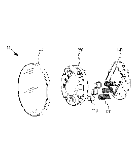
FIG. 3 shows a further exploded perspective view of the interface 10 with the
capacitive touch sensors 100.The display cover 14 and the transmitter 16 are
not shown
for clarity. The capacitivetouch sensors 100 include electrodes 110 disposed
between a
plate120 and springs 130. Although not shown, the plate 120 is coupled to the
display
cover 14 described in the foregoing with reference to FIG. 2. Three electrodes
110 and
springs 130 are shown although more or fewer may be employed in alternative
embodiments. The capacitive touch sensor 100 also includes a circuit board 140
that
processes signals, such as electrical signals, from the electrode 110. The
circuit board
140 is coupled to a panel 150. In the embodiment shown, the signalsarecoupled
to the
circuit board 140 via the springs 130 although alternative embodiments may
employ a
separate signal path such as a flex circuit. The operator inputs data by
touching the front
of the plate 120 where the capacitive touch sensors 100 are located.
FIG. 4 shows an exploded perspective view of a simplified model of the
capacitive touch sensor 100 for clarity. The simplified model shows a single
capacitive
touch sensor 100 with disks representing portions of the plate 120 and the
circuit board
140. The panel 150is not shown so the electrode 110 and the spring 130 canbe
viewed
without obstruction. However, in alternative embodiments, the panel 150 may
not be
employed.As shown in FIG. 4, the capacitivetouch sensor 100 includes the
electrode
110 that is disposed between the plate 120 and the spring 130. In the
embodiment shown,
the spring 130 can hold the electrode 110 spaced apart from the circuit board
140.
6
CA 02944526 2016-09-30
WO 2015/149324 PCT/CN2014/074715
The electrode 110 includes a sensing surface 112. As shown, the sensing
surface
112 is flat and parallel with the plate 120. The sensing surface 112 is also
shown with a
circular shape although any suitable shape may be employed in alternative
embodiments.
The electrode 110 also includes an extending portion 114 that extends from
away from
the sensing surface 112 in a perpendicular direction. The extending portion
114 has a
cylindrical shape although any suitable shape can be employed. A shoulder 116
is at a
distal end of the extending portion 114. Although shown as displaced away from
the
plate 120 in the exploded view, the sensing surface 112 can be proximate to or
touching
the plate 120.
In the embodiment shown, the plate 120 is a dielectric material such as glass.
The
material can be selected for electrical as well as mechanical properties. For
example, the
plate 120 can be comprised of a glass that has a desired dielectric constant.
The
dielectric constant can be selected tobe, for example, relatively highto
ensure that the
capacitive touch sensor 100 operates reliably when the operator touches
against the plate
120. The glass can also have mechanical properties (e.g., strength, toughness,
etc.) that
are suitable for use in hazardous and uncontrolled environments that could,
for example,
cause material to strike the plate 120. The electrode 110 is pressed towards
the plate 120
by the spring 130.
The spring 130 is shown as a coil spring that is disposed between the
electrode
110 and the circuit board 140.However, in alternative embodiments, the spring
130 can
have different shapes and configurations. For example, an alternative
springcould be
conductive foam with a cylinder shape. The spring 130 also includes a distal
portion 132.
The distal portion 132 can mechanically and electrically couple the spring 130
to the
circuit board 140. However, in alternative embodiments, the distal portion 132
can
mechanically couple the spring 130 to something other than the circuit board
140.
Additionally or alternatively, a conductor, such as a flex circuit, can
electrically couple
the electrode 110 with the circuit board 140. The distal portion 132 is shown
as
including posts 132p that interface with the circuit board 140.
The circuit board 140 shown with a pair of openings 142a,b although more or
fewer openings can be employed. The circuit board 140 can include components,
such
as memory chips and processors, traces, or the like. As shown, the openings
142a,b
areconfigured to accept the posts 132p. In alternative embodiments, soldering
tabs rather
7
CA 02944526 2016-09-30
WO 2015/149324 PCT/CN2014/074715
than the openings 142a,b can be employed.The posts 132p can extend into the
openings
142a,b. Solder can be applied to the posts132p and the circuit board 140 to
mechanically
and electrically couple the spring 130 with the circuit board 140. The
electrode 110 and
the spring 130 are described in more detail in the following with reference to
FIGS. 5a
and 5b.
FIGS. 5a and 5b show an enlarged perspective view of the electrode 110 and an
enlarged side view of the spring 130, respectively. As can be seen in FIG. 5a,
the
extending portion 114 extendsperpendicularly away from the sensing surface
112. In
alternative embodiments, the extending portion 114 can extend away from the
sensing
surface 112 in non-perpendicular directions and have different shapes. For
example, the
extending portion could extend away from the sensing surface 112 as a post
that is
configured to fit within, rather than surrounding, the spring 130.The spring
130 is shown
as having distal portions 132, 134. Between the distal portions 132, 134 are a
partial
cone portion 136 and a cylindrical portion 138. The spring 130 also has a
longitudinal
length L. As can be seen, the distal portion 134 has an inverse cone region
with a higher
turn-per-length ratio than the partial cone portion 136 and the cylindrical
portion 138.
However, any appropriate turn ratios can be employed. The shape and dimensions
of the
electrode 110 and the spring 130 can be selected so the electrode 110 does not
move
relative to the plate 120, as will be described in more detail in the
following.
FIG. 6 shows a cross sectional side view of the capacitive touch sensor 100
taken at 6-6 in FIG. 4.A simplified version of the panel 150 is shown. The
extending
portion 114 surrounds a portion of the spring 130.The spring 130 is coupled to
the
circuit board 140 via the posts 132p. Although not shown, solder can be
applied to the
posts 132p and the circuit board 140 to affix the spring 130 to the circuit
board 140. The
solder can also electrically couple the spring 130 to the circuit board 140.
In the
embodiment shown, the interior diameter of the extending portion 114 can be
sized and
dimensioned to interface with the spring 130. For example, the internal
diameter of the
extending portion 114 can be approximately the same as the largest diameter of
the
distal portion 134. The electrode 110 is coupled (e.g., slidably) to the panel
150.
Additionally or alternatively, the electrode 110 can be fitted into the panel
150. Also
shown is a shoulder 116 on the extending portion 114 that can press against a
portion of
the panel 150.
8
CA 02944526 2016-09-30
WO 2015/149324 PCT/CN2014/074715
The panel 150is shown as a rectangular cross section of a cylindrical shape
having an opening. The electrode 110 can be disposed in the opening. The panel
150is
also shown with an end portion 152 that is sized about the same as the
shoulder 116.
Alternative shapes and cross sections can be employed. For example, an L-
shaped
bracket that is attached to the panel can be employed in alternative
embodiments.
Additionally, the panel 150is shown as coupled to the circuit board 140.
However, the
electrode 110 can interface with alternative brackets that are coupled to, for
example,
the display cover 14. These and other interfaces can prevent movements and
variations
in relative positions in the capacitive touch sensor 100.
Movements in a direction parallel to the longitudinal length L of the spring
130
can be prevented. For example, the spring 130 can press the electrode 110
against the
plate 120. Accordingly, a friction force can be formed that is parallel to the
sensing
surface 112.The friction force can prevent a movement that is perpendicular to
the
longitudinal length L of the spring 130. The interface between the distal
portion 134 and
the internal diameter of the extending portion 114 can also prevent the
movement of the
electrode 110 perpendicular to the longitudinal length L. For example, the
distal portion
134 can be fitted into the extending portion 114. This interface can prevent
the electrode
110 from moving relative to the spring 130. Additionally or alternatively, the
panel
150can prevent the movement of the electrode 110 in the direction
perpendicular to the
longitudinal length L of the spring 130.The extending portion 114 interfacing
with the
panel 150can prevent the electrode 110 from moving relative to the panel 150.
Movement parallel to the longitudinal length L can also be prevented. For
example, the electrode 110 can be pressed against the plate 120 where the
sensing
surface 112 is parallel to the plate 120. The force can be sufficient to
prevent the
electrode 110 from displacing away from the plate 120 when, for example, the
interface
lOis being vibrated. The shoulder 116 is shown as interfacing the panel 150and
the
electrode 110 as pressed against the plate 120. However, in alternative
embodiments, the
shoulder 116 may not interface the panel 150. For example, a gap can be formed
between the panel 150and the shoulder 116 when the electrode 110 presses
against the
plate 120. Alternatively, the shoulder 116 can prevent a movement of the
electrode 110
in a direction that is parallel to the longitudinal length L of the spring
130. Accordingly,
a gap may be formed between the electrode 110 and the sensing surface 112.
9
CA 02944526 2016-09-30
WO 2015/149324 PCT/CN2014/074715
Variations in the relative positions in the capacitive touch sensor 100 can be
reduced. For example, during assembly of the interface 10, the electrode 110
can be
inserted into the panel 150and the spring 130 inserted into the electrode 110.
The circuit
board 140 can be coupled to the spring 130 and the panel 150. As can be
appreciated,
the extending portion 114 and the shoulder 116 can interface with the panel
150to align
the electrode 110. Accordingly, the electrode 110 does not move in a direction
perpendicular to the longitudinal length L of the spring 130. This ensures
that the
relative position of the each electrode 110 with respect to each other and the
panel
150does not change on an assembly to assembly basis (e.g., the positions are
repeatable).
Variations in other relative positions in the capacitive touch sensor 100 can
also be
reduced. For example, the distal portion 134 can interface with the internal
diameter of
the extending portion 114. This can prevent variations in the relative
positions of the
sensing surface 112 and the spring 130.
Preventing movements and reducing variation in the relative positions in the
capacitive touch sensor 100 can reduce variations in the electrical properties
of the
capacitive touch sensor 100. For example, preventing the movement of the
sensing
surface 112 relative to the plate 120 prevents movement of the sensing surface
112
relative to the operator O's finger (shown in FIG. 7). The relative positions
of the
sensing surface 112 and the operator O's finger is therefore the same when the
operator
0 places the finger in the same location. As a result,the change in the
capacitance of the
electrode 110is the same each time the operator 0 presses the capacitive touch
sensor
100 at the same location. Similarly, the relative positions of the electrode
110 with other
electrodes, as well as thepanel 150,do not vary. Reducing variation in the
electrical
properties in the capacitive touch sensor 100 can also improve the reliability
of the
capacitive touch sensor 100, as will be discussed in more detail in the
following.
FIG. 7 shows an electrical block diagram of the capacitive touch sensor 100
according to an embodiment. The capacitive touch sensor 100 is shown with a
signal
path 710 coupled to the electrode 110 and the circuit board 140.Also shown is
a pulse
signal 720 that is generated by the circuit board 140. The pulse signal 720 is
sent to the
electrode 110 via the signal path 710. Also shown are a samplecapacitor Cs and
a
sampling path 730. The capacitive touch sensor 100 is shown with field lines
that radiate
from electric charges in the electrode 110.The field lines radiate through the
plate 120.
CA 02944526 2016-09-30
WO 2015/149324 PCT/CN2014/074715
When an operator 0 moves a finger (or some other object) on the front surface
of
the plate 120, the field lines bend into the finger thereby coupling the
electrode to the
environment. This causesthe capacitance of the electrode 110 to change (e.g.,
increase)
so the pulse signal 720 will change. This change in capacitance is sensed by
the circuit
board 140 through the sample capacitor Cs and the sampling path 730. The
change in
capacitance of theelectrode 110 can be small and vary due to factors such as
thickness
and dielectric constant of the plate 120, width and surface smoothness of the
electrode
110, the capacitance of the capacitor Cs, the length of the signal path 710,
and the
touched area width of the operator O's finger on the plate 120.
The signal path 710 can have a physical length that is proportional to the
longitudinal length L of the spring 130 and the spaced relationship between
the
electrode 110 and the circuit board 140.The spaced relationshipcan improve the
ability
of the capacitive touch sensor 100 to withstand the hazardous and uncontrolled
environments. For example, in the embodiment described with reference to FIGS.
1-6,
the circuit board 140 is disposed behind both the plate 120 and the panel 150.
This can
protect the circuit board 140 from the environment. However, a long signal
pathcan
distort the shape ofthe pulse signal 720 thereby affecting the sensing of the
operator O's
finger.
Preventing variation and movement in the electrode 110 ensures that the
capacitance change is substantially the same each time the operator O's finger
touches
the plate 120. For example, by preventing the movement of the electrode 110
away from
the plate 120 during use, the distance from the sensing surface 112 to the
surface S of
the plate 120 remains the same. Accordingly, when theinterface 10 is vibrating
due to,
for example, vibrations in a mounting fixture, the distance between the
operator O's
finger and the sensing surface 112 remains the same. Similarly, the spring 130
presses
the electrode 110 into the plate 120 with sufficient force to prevent the
electrode 110
from moving in a direction perpendicular to the longitudinal length L of the
spring 130.
Additionally or alternatively, the extending portion 114 can interface with
the spring
130 and the panel 150to prevent the electrode 110 from moving perpendicular to
the
longitudinal length L. The electric properties of the electrode 110,
therefore, do not vary
as a result of the electrode 110 moving relative to the plate 120.
11
CA 02944526 2016-09-30
WO 2015/149324 PCT/CN2014/074715
Dimensions as well as electrical and mechanical properties can also be
selected
to ensure that the capacitive touch sensor 100 reliably detects the operator
O's finger.
For example, a uniform and flat distribution of the charges in the electrode
110 can
improve the reliability of the capacitive touch sensor 100. The charges may be
uniformly distributed in the electrode 110 by using a conductor with
sufficient
conductivity. The charges can have the flat distribution due to the flat
sensing surface
112.The flat distribution ensures that the field lines are substantially
uniform within the
diameter of the sensing surface 112.If the field lines varied within the width
of the
sensing surface 112, small changes in the position of the operator O's finger
within the
diameter of the sensing surface 112 can result in different capacitance of the
electrode
110.
The width of the sensing surface 112 can also be selected to improve the
reliability of the capacitive touch sensor 100. For example, a relatively wide
sensing
surface 112 ensures that the operator 0 can place the finger in various
locations within
the width of the sensing surface 112 without producing different capacitance
values. For
example, near the edge of the sensing surface 112, the field lines are
typically bent
outwards as shown. At a distance from the edge of the sensing surface 112, the
field
lines are vertically oriented and uniform. Due to the width of the sensing
surface 112,
the field lines bend with a substantially same shape as the operator O's
finger moves
from the center towards the edge of the sensing surface. When the operator O's
finger
bends the field lines that are not uniform and vertically oriented, the
capacitance value
of the sensing electrode 110 is not the same as when the operator O's finger
is in the
center of the sensing surface 112. The wide sensing surface 112 allows the
capacitance
change of the electrode 110 to be the same even if the operator 0 presses
against the
surface S of the plate 120 in different locations.
The thickness t of the plate 120 can also be selected to provide desired
electrical
and mechanical properties. For example, the field lines from the charges in
the sensing
surface 112 can be substantially uniform for a plate 120 with a selected
thickness that is
relatively thin. The selected thickness can also have sufficient mechanical
strength to
withstand hazardous and uncontrolled environments. The selected thickness can
therefore allow the capacitive touch sensor 100 to reliably sense the operator
O's finger
in a wide range of environmental conditions.The thickness t can be selected
along with
12
CA 02944526 2016-09-30
WO 2015/149324 PCT/CN2014/074715
the material's dielectric strength to ensure that the field is sufficiently
strong at the
surface S.
In operation, the interface 10 can be installed and coupled to a flow meter
installed on a pipeline. The interface 10 can be installed in various
locations such as
directly coupled to the flow meter, coupled to the pipeline, affixed to a
wall, or the like.
The flow meter can measure and provide data on the properties of materials in
the
pipeline. The data can be received by the interface 10.An operator 0 can touch
the
interface 10 to obtain data or control parameters in the flow meter. The
operator O's
touch can be reliably sensed by the capacitive touch sensor 100 in various
environmental conditions.
The capacitive touch sensor 100 can detect the operator 0's finger by sensing
the
capacitance of the electrode 110 change. More specifically, the operator O's
finger
bends the field lines from the charges in the electrodes 110 to change the
capacitance of
the electrode 110. The change in capacitance can be detected by the circuit
board 140.
For example, in an embodiment, pulse signal 720 can be sent through the signal
path
710. The change in capacitance of the electrode 110 and the pulse signal 720
can cause a
return signal to be sent through the sampling capacitor Cs and the sampling
path 730.
The circuit board 140 can detect the return signal to sense the operator O's
finger.
The embodiments described above provide a capacitive touch sensor 100. As
explained above, the capacitive touch sensor 100 can reliably operate in a
wide range of
environmental conditions. For example, the field lines can be substantially
uniform
along the surface S of the plate 120. The capacitance change due to the
operator O's
finger is therefore the same within the width of the sensing surface 112. In
addition,
although the interface 10 may be subjected to vibration, the position of the
electrode 110
relative to the surface S of the plate 120 remains the same. The relative
position is the
same due to, for example, the spring 130 pressing the electrode 110 against
the plate 120.
The relative position can also be the same due to the extending portion 114
interfacing
with the spring 130 and/or the panel 150. The sensing surface 112 can also
have width
that is sufficiently large that the capacitance change remains the same even
if the
operator O's finger can touch the surface S of the plate 120 at different
locations. The
plate 120 is also thick enough to withstand impacts and other adverse
conditions from
the environment.
13
CA 02944526 2016-09-30
WO 2015/149324 PCT/CN2014/074715
The detailed descriptions of the above embodiments are not exhaustive
descriptions of all embodiments contemplated by the inventors to be within the
scope of
the present description. Indeed, persons skilled in the art will recognize
that certain
elements of the above-described embodiments may variously be combined or
eliminated
to create further embodiments, and such further embodiments fall within the
scope and
teachings of the present description. It will also be apparent to those of
ordinary skill in
the art that the above-described embodiments may be combined in whole or in
part to
create additional embodiments within the scope and teachings of the present
description.
Thus, although specific embodiments are described herein for illustrative
purposes, various equivalent modifications are possible within the scope of
the present
description, as those skilled in the relevant art will recognize. The
teachings provided
herein can be applied to other touch sensors, and not just to the embodiments
described
above and shown in the accompanying figures. Accordingly, the scope of the
embodiments described above should be determined from the following claims.
14