Note: Descriptions are shown in the official language in which they were submitted.
CA 02944710 2016-09-30
WO 2015/195199
PCT/US2015/026601
EGRESS AND/OR FLICKER-FREE LIGHTING DEVICE WITH PERSISTENT
LUMINESCENCE
TECHNICAL FIELD
[0001] The technical field relates generally to a lighting device
integrally formed of layers
with a plurality of light-emitting elements sandwiched in a layer(s). More
particularly, the
technical field relates to structure in which the integral layer(s) that has
the light-emitting
elements is doped to provide persistent luminescence.
BACKGROUND
[0002] A majority of lighting devices directed to egress application
technology that use
afterglow, comprise photo-excited films which are painted on a desired
structure. A
conventional application is for egress lighting, for buildings, for aerospace
applications, and
so on. The conventional film painted on the application has to be painted from
the outside
onto the structure, from sources that are around the structure. The film in
conventional
devices is always painted onto whatever is the long-lived emission.
[0003] The film and the paint are excited by the light absorbed from the
environment.
These materials are conventionally used to indicate an exit after a light is
off This leaves the
known afterglow film as the only option, for example, for people to find the
exit, in a manner
which is consequently dependent on the time of the excitation and the power of
the
excitation.
SUMMARY
[0004] In accordance with one or more embodiments, a lighting device
includes a
substrate; two or more light-emitting elements formed over the substrate; an
affixing layer
fixing the two or more light-emitting elements in place; and a transparent
conductive layer in
electrical contact with the light-emitting elements. The substrate and the
transparent
conductive layer sandwich the affixing layer with the light-emitting elements
in place. The
affixing layer is an electrically insulating material. The affixing layer is
doped with a photo
active or photochromic material. In a first mode when the light-emitting
elements are
energized, the photo active or photochromic material of the affixing layer is
excited by the
light-emitting elements. In a second mode when the light-emitting elements are
de-
energized, the affixing layer produces a persistent luminescence.
[0005] In another embodiment, in the first mode, while using AC voltage to
drive the
light-emitting elements, during the off-cycle of the AC, the light-emitting
elements are off
CA 02944710 2016-09-30
WO 2015/195199
PCT/US2015/026601
and the affixing layer surrounding the light-emitting elements produces the
persistent
luminescence for at least a duration of the off-cycle of the AC, to avoid
flickering during the
off-cycle.
[0006] In yet another embodiment, the transparent conductive layer is semi-
transparent
and bounces at least some of the light from the light-emitting elements back
into the affixing
layer to further excite the affixing layer to produce additional persistent
luminescence.
[0007] In still another embodiment, the lighting device further includes a
semi-transparent
layer sandwiching the transparent conductive layer, the semi-transparent layer
bounces at
least some of the light from the light-emitting layer back into the affixing
layer to further
excite the affixing layer to produce additional persistent luminescence.
[0008] In a further embodiment, the light-emitting elements can be oriented
any direction
in the affixing layer, to emit the persistent luminescence when the lighting
device is powered
down.
[0009] In yet a further embodiment, the wave length of the light-emitting
elements is UV
or blue.
[0010] In still a further embodiment, the affixing layer includes non-doped
areas to
comprise a pattern of a pre-determined non-persistent-luminescent area.
[0011] Another embodiment provides an emergency light. The emergency light
includes
one or more combinations of embodiments of the above lighting device, driven
by DC
voltage. In a power-on mode the DC voltage drives the light emitting elements.
In a power-
off mode, the DC voltage does not drive the light emitting elements, and the
affixing layer
acts as a persistent luminescent marker.
[0012] In accordance with another embodiment, there is provided a lighting
device, which
includes a substrate; two or more light-emitting elements formed over the
substrate; a
protective surrounding layer fixing the two or more light-emitting elements in
place. The
protective surrounding layer is doped with a photo active or photochromic
material. In a first
mode when the light-emitting elements are energized, the photo active or
photochromic
material of the affixing layer is excited by the light-emitting elements. In a
second mode
when the light-emitting elements are de-energized, the affixing layer produces
a persistent
luminescence.
[0013] In another embodiment, in the first mode, while using AC voltage to
drive the
light-emitting elements, during the off-cycle of the AC, the light-emitting
elements are off
and the protective surrounding layer surrounding the light-emitting elements
produces the
CA 02944710 2016-09-30
WO 2015/195199
PCT/US2015/026601
persistent luminescence for at least a duration of the off-cycle of the AC, to
avoid flickering
during the off-cycle.
[0014] Yet another embodiment further includes a semi-transparent layer
sandwiching the
protective surrounding layer, the semi-transparent layer bounces at least some
of the light
from the light-emitting layer back into the protective surrounding layer to
further excite the
protective surrounding layer to produce additional persistent luminescence.
[0015] In still another embodiment, the light-emitting elements can be
oriented any
direction in the protective surrounding layer, to emit the persistent
luminescence when the
lighting device is powered down.
[0016] In a further embodiment, the wave length of the light-emitting
elements is UV
and/or blue.
[0017] According to another embodiment, there is provided an emergency
light. The
emergency light includes one or more combinations of embodiments of the above
lighting
device, driven by DC voltage. In a power-on mode the DC voltage drives the
light emitting
elements. In a power-off mode, the DC voltage does not drive the light
emitting elements,
and the protective surrounding layer acts as a persistent luminescent marker.
[0018] According to still another embodiment, there is a method of forming
a lighting
device. The method includes providing a substrate; forming two or more light-
emitting
elements over the substrate; forming an affixing layer on the substrate fixing
the two or more
light-emitting elements in place; and forming a transparent conductive layer
over the affixing
layer. The substrate and the transparent conductive layer sandwich the
affixing layer with the
light-emitting elements in place. The affixing layer is an electrically
insulating material. The
affixing layer is doped with a photo active or photochromic material. In a
first mode when
the light-emitting elements are energized, the photo active or photochromic
material of the
affixing layer is excited by the light-emitting elements. In a second mode
when the light-
emitting elements are de-energized, the affixing layer produces a persistent
luminescence
when energized.
[0019] In an embodiment of the method, the transparent conductive layer is
semi-
transparent and bounces at least some of the light from the light-emitting
elements back into
the affixing layer to further excite the affixing layer to produce additional
persistent
luminescence.
[0020] An embodiment of the method can further include forming a semi-
transparent
layer on the transparent conductive layer, in which the semi-transparent layer
bounces at least
CA 02944710 2016-09-30
WO 2015/195199
PCT/US2015/026601
some of the light from the light-emitting layer back into the affixing layer
to further excite the
affixing layer to produce additional persistent luminescence.
[0021] In another embodiment of the method , the wave length of the light-
emitting
elements is UV or blue.
[0022] Still another embodiment can include pre-forming the affixing layer
to include
non-doped areas to comprise a pattern of a pre-determined non-persistent-
luminescent area.
[0023] In accordance with various embodiments, there may be provided a
method of
forming a lighting device. The method can included providing a substrate;
forming two or
more light-emitting elements over the substrate; and forming a protective
surrounding layer
on the substrate with the two or more light-emitting elements, the protective
surrounding
layer fixes the two or more light-emitting elements in place. The protective
surrounding
layer is doped with a photo active or photochromic material. In a first mode
when the light-
emitting elements are energized, the photo active or photochromic material of
the protective
surrounding layer is excited by the light-emitting elements. In a second mode
when the light-
emitting elements are de-energized, the protective surrounding layer produces
a persistent
luminescence.
[0024] The method can further include forming a semi-transparent layer on
the protective
surrounding layer, the semi-transparent layer bounces at least some of the
light from the
light-emitting layer back into the protective surrounding layer to further
excite the protective
surrounding layer to produce additional persistent luminescence.
[0025] In an embodiment of the method, the wave length of the light-
emitting elements is
UV and/or blue.
BRIEF DESCRIPTION OF THE DRAWINGS
[0026] The accompanying figures where like reference numerals refer to
identical or
functionally similar elements and which together with the detailed description
below are
incorporated in and form part of the specification, serve to further
illustrate an exemplary
embodiment and to explain various principles and advantages in accordance with
the
embodiments. These drawings are not necessarily drawn to scale.
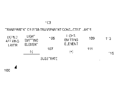
[0027] FIG. 1 is a cross-sectional view of a lighting device with light-
emitting elements in
an affixing layer according to a first embodiment;
[0028] FIG. 2A is a cross-sectional view of the lighting device showing
excitation of the
doped affixing layer;
[0029] FIG. 2B is a cross-sectional view of the lighting device showing
persistent
luminescence with de-energized light-emitting element;
CA 02944710 2016-09-30
WO 2015/195199
PCT/US2015/026601
[0030] FIG. 3 is a timing diagram illustrating timing of alternating
current ("A/C") power
and persistent luminescence;
[0031] FIG. 4 is a cross-sectional view of a lighting device according to a
second
embodiment with a semi-transparent layer;
[0032] FIG. 5 is a cross-sectional view of a lighting device according to a
third
embodiment;
[0033] FIG. 6A and FIG. 6B (collectively, FIG. 6) are a plan view of a
lighting device in a
powered on mode and a powered off mode, with a pattern of non-persistent
luminescent
areas, according to a fourth embodiment;
[0034] FIG. 7 is a cross section along line VII of the lighting device of
FIG. 6B;
[0035] FIG. 8A to FIG. 8D are cross sections of a lighting device
illustrating a method of
forming the lighting device; and
[0036] FIG. 9A to FIG. 9F are cross sections of a lighting device with a
pattern of
persistent and non-persistent luminescent areas, illustrating a method of
forming the lighting
device.
DETAILED DESCRIPTION
[0037] In overview, the present disclosure concerns lighting devices, used
for applications
such as egress lighting or in an application sensitive to flickering, for
example in LED
lighting. More particularly, various inventive concepts and principles are
embodied in
lighting devices, systems, and methods therein in which an extra component may
be included
in a remote phosphor, remote emissive material, or adhesive, to contain a long
lived radiative
emission, which can avoid the flickering routinely observed in LED lighting.
[0038] A specific LED application can comprise a combination of an LED, for
example in
a form of a flexible strip, and a photo-luminescent material, in which the
luminescent
material is embedded within the coating of the device, for example a polymer
coating, and
the excitation for the lighting device also comes from within the polymer
coating.
[0039]
[0040] The instant disclosure is provided to further explain in an enabling
fashion the best
modes of performing one or more embodiments. The disclosure is further offered
to enhance
an understanding and appreciation for the inventive principles and advantages
thereof, rather
than to limit in any manner the invention. The invention is defined solely by
the appended
claims including any amendments made during the pendency of this application
and all
equivalents of those claims as issued.
CA 02944710 2016-09-30
WO 2015/195199
PCT/US2015/026601
[0041] It is further understood that the use of relational terms such as
first and second, and
the like, if any, are used solely to distinguish one from another entity,
item, or action without
necessarily requiring or implying any actual such relationship or order
between such entities,
items or actions. It is noted that some embodiments may include a plurality of
processes or
steps, which can be performed in any order, unless expressly and necessarily
limited to a
particular order; i.e., processes or steps that are not so limited may be
performed in any order.
[0042] Furthermore, elements having the same number represent the same
element across
the various figures, and throughout the disclosure. Their description is not
always repeated
for each embodiment, but may be inferred from previous descriptions. Elements
that have the
same number but have the addition of a letter designator indicate distinct
embodiments of a
more generic element.
[0043] As further discussed herein below, various inventive principles and
combinations
thereof are advantageously employed to reduce constraints on the usable time
since the
excitation source will come from within the afterglow-containing film. The
LEDs will excite
the film. The lighting may be run with battery power, if desired, which can be
turned on
and/or off thereby providing a longer time for the afterglow, for the
protection of the end
users.
[0044] Further in accordance with exemplary embodiments, a long lived
material can be
used, for example in an AC lighting application. The long lived luminescent
material can be
embedded in an adhesive or mixed with a remote emissive material to create a
flicker-free
LED lighting solution, for example, when the LEDs are driven directly from an
AC source
without the use of electronics to power up the LEDs while the waveform drops
to zero volts.
The typical "flicker" normally observed in conventional devices will not be
noted since it will
be asked by the long lived emissive decay process of the materials.
[0045] Moreover, the lighting device can be used for egress lighting, for
buildings, for
aerospace applications, etc. In such applications, the conventional film
painted on the
application has to be painted from the outside onto the structure; the film
that is painted on a
conventional device is what provides the long-lived emission. Here, the
present lighting
device does not use a film or paint which is applied to a structure, but it is
an adhesive which
is a physically integral part of the lighting device structure, which produces
the persistent
luminescence.
[0046] First Embodiment
[0047] Referring now to FIG. 1, a cross-sectional view of a lighting device
with light-
emitting elements in an affixing layer according to a first embodiment will be
discussed and
CA 02944710 2016-09-30
WO 2015/195199
PCT/US2015/026601
described. A lighting device 100 can include a conductive layer 103, light
emitting elements
105, 109, first and second electrical connections 107, 111, an affixing layer
113, and a
substrate 115.
[0048] The substrate 115 can serve as a base for the remainder of the
lighting device 100.
As a reference direction, the substrate 125 can be considered to be a "bottom"
substrate upon
which the other elements are stacked. However, this is as a point of reference
only. The
lighting device 100 has no inherent direction, and can be oriented in any
manner, even with
the substrate 115 being on the "top" of the structure.
[0049] The substrate 115 can be made of polyethylene terephthalate (PET),
polyethylene
napthalate (PEN), polyester, a polymer, an oxide-coated polymer, a flexible
plastic, a metal-
coated flexible plastic, or any suitable material. In some embodiments, the
substrate 115 may
be flexible. If the entire lighting device is to be flexible, then the
substrate 115 should be
flexible. Because light does not shine out of the substrate 115, it is not
necessary for the
substrate 115 to be transparent to light.
[0050] The first and second electrical connections 107, 111 are located on
the substrate
115. Each of the first and second electrical connections 107, 111 can be made
of a
conductive material that can be connected to a control circuit used to control
the lighting
device 100, and can be configured to carry a control current generated by the
control circuit.
For example, the first and second electrical connections 107, 111 may be buss
bars used to
conduct electricity throughout a lighting device 100. In alternate embodiments
the first and
second electrical connections 107, 111 may be wires or any other conductive
structure that
can pass current to the light-emitting element 105, 109. The first and second
electrical
connections may further be connected using: silver epoxy dots, conductive
adhesive, metal
pads, or other conductive metal elements. The first and second electrical
connections 107,
111 may be made of copper, silver, aluminum, or any suitable conductive metal
or
conductive oxide. If the resulting lighting device 100 must remain flexible,
the first and
second conductive elements 107, 111 can be configured such that they can bend
without
breaking or losing their ability to carry a current.
[0051] The conductive layer 103 can be a transparent or semi-transparent
conductive
layer, using known techniques and conventional materials. In this embodiment,
the
transparent or semi-transparent conductive layer 103 is used to close the
electrical circuit to
the light emitting elements 105, 109. The conductive layer 103 can be, for
example, a
transparent conductive oxide (TCO) layer made of indium tin oxide, tin oxide,
zinc oxide,
carbon nanotubes, ultra-thin metals, or any suitable transparent, conductive
material.
CA 02944710 2016-09-30
WO 2015/195199
PCT/US2015/026601
[0052] It is generally desirable that the affixing layer be substantially
transparent to the
wavelengths of light that are emitted from the light-emitting element 105,
109, so that light
from the light-emitting elements 105, 109 can pass through the affixing layer
113.
[0053] The affixing layer 113 can be doped with a photo active or
photochromic material
which is a material that provides a luminescent emission or changes its color
after
excitation. The photo active material can provide a short-lived to a long-
lived emission after
excitation, with an emission decay at least from a microsecond regime all the
way up to
hours. A long lived material can be used. The material could be doped into an
adhesive or
mixed with a remote emissive material. Chemicals used for doping with the
photo active or
photochromic material are fairly standard and are generally commercially
available. Appropriate photochromic materials include, for example,
spiropyrans,
diarylethers, quinones derivatives, azobenzenes families of compunds or
inorganic
salts. Appropriate materials for doping the affixing layer with a photo active
material
include long lived emission materials; the long lived emission materials can
be, for example,
gold complexes, cadmium or zinc sulfides doped with copper, or newer materials
as
strontium oxide-based compounds or heavy-atom-doped organic materials or pure
organic
phosphors. The doping material can be doped into different materials which
will work for the
same purposes, i.e., as the affixing material.
[0054] The light emitting elements 105, 109 are conventionally available.
The light-
emitting element 105, 109 can be configured to generate light based on the
control current
carried on the first and second electrical connections 107, 111. One exemplary
light-emitting
element 105, 109 is a light-emitting diode (LED). An LED has an anode (i.e., a
positive side)
and a cathode (i.e., a negative side), and operates to generate light of a
specific wavelength
(from infrared to ultraviolet, i.e., having a wavelength from 10 nm to 100,000
nm) when
current flows through the LED from the anode to the cathode. Appropriate
ranges of
wavelengths for the light emitting elements 105, 109 are between UV and blue.
Thus, in an
embodiment, the wave length of the light-emitting elements is UV or blue.
Thus, there can
be different colors used for the persistent luminescent materials. The reason
for using the
different wavelengths is so that the light is visible, or so that the light
can be moved from
blue to a different color.
[0055] The light emitting elements 105, 109 can be formed over the
substrate 115, and are
in the affixing layer 113. The lighting emitting elements 105, 109 can be pre-
formed into a
desired pattern within the lighting device 100, using known techniques.
CA 02944710 2016-09-30
WO 2015/195199
PCT/US2015/026601
[0056] The light emitting elements are electrically connected to the
conductive layer 103
and the substrate 100 via positive and negative electrical connections 107,
111.
[0057] By comparison, in the fixing layer of a traditional device,
conventionally there is
provided a hot melt which acts as the adhesive to keep the top and bottom
substrates with
LED chips sandwiched together. For example, in the traditional device
illustrated in US
7,052,924 to Daniels et al. (Daniels), an adhesive matrix, into which emissive
particulate
such as LED chips are embedded, secures top and bottom substrates. Sometimes,
a
traditional device includes UV LED chips and a phosphor re-emitter additive
dispersed in the
matrix between the substrates, the re-emitter additive being in essence short-
lived after
excitation in AC mode. Such a traditional device can experience flicker
because of the short-
lived excitation.
[0058] In the present application, for example as in the lighting device
100, the material
which comprises the affixing layer, for example, hot melt, is loaded with a
long lifetime
luminescent material which is selected because it will glow in the dark, for a
long time.
When the lighting device is powered on, the lighting device excites the
molecules in the
polymer with the light coming from the light emitting elements 105, 109. When
the light is
powered off, the light provides a persistent luminescence from the doped
affixing layer 113.
[0059] In summary, the lighting device 100 includes the substrate 115, the
affixing layer
113, and the light emitting elements 105, 109 (sometimes referred to as LEEs
or LEDs) are
embedded in the affixing layer 113. An indium tin oxide (ITO) product can be
part of one of
the layers, for example the transparent or semi-transparent conductive layer
103, in
accordance with known techniques, to provide an electrical connection between
light emitting
elements 105, 109. The transparent or semi-transparent conductive layer 103
can be provided
with or without phosphor.
[0060] The affixing layer 113 can be, for example, formed from a
conventional hot melt
that mechanically fixes the elements together and keeps them in place. The
affixing layer
113 can be an electrical insulator. The conductive path, from the substrate
115 to the
transparent conductive layer 103, flows through the light emitting elements
105, 109. The
affixing layer, such as an adhesive, or for example a hot melt, flows around
the different
elements so that the elements of the conductive path are mechanically touching
and
electrically connected so as to create a pathway from the transparent
conductive layer 103 to
the bottom substrate 100 through the light-emitting elements 105, 109. Thus,
the source of
the excitation of the doped affixing layer comes from within the affixing
layer itself
CA 02944710 2016-09-30
WO 2015/195199
PCT/US2015/026601
[0061] FIG. 2A and FIG. 2B illustrate excitation of the doped affixing
layer with the
energized light emitting elements, and persistent luminescence with the de-
energized light
emitting elements, in first and second modes, respectively. Referring now to
FIG. 2A, a
cross-sectional view of the lighting device showing excitation of the doped
affixing layer will
be discussed and described. In review, a lighting device can include a
conductive layer 203,
light emitting elements 205, 209, electrical connections 207, 211, an affixing
layer 213, and a
substrate 215. The two light-emitting elements 205, 209 are representative of
two or more
light-emitting elements formed over the substrate 215, which can be provided
according to
conventional techniques; there is an affixing layer 213 which fixes the two or
more light-
emitting elements 205, 209 in place (generally the structure can be provided
in accordance
with conventional techniques).
[0062] Also, there is a transparent or semi-transparent conductive layer
203, which also
can be provided according to conventional techniques. This layer is
transparent or semi-
transparent to light from the light-emitting elements 205, 209. The substrate
215 and the
transparent conductive layer 203 sandwich the affixing layer 213 with the
light-emitting
elements 205, 209 in place according to known techniques. The top layer 203
can be semi-
transparent to further bounce some of the light from the affixing layer, which
can be
transparent and thus can emit light, back into the affixing layer to produce
additional
luminescence. Thus, the semi-transparent conductive layer bounces at least
some of the light
from the light-emitting elements back into the affixing layer to further
excite the affixing
layer to produce additional persistent luminescence.
[0063] The affixing layer 213 is doped with a photo active or photochromic
material that
is excited by the light-emitting elements 205, 209 in a first mode when the
light-emitting
elements are energized. The electrically insulating material of the affixing
layer 213 can be
excited with the light from the light emitting elements 205, 209. Although the
light from the
energized light-emitting elements 205, 209 can be principally emitted through
the transparent
conductive layer 203, some of the light from the LEE's bounces to the
transparent conductive
layer 203, and then moving to the side and then back into the affixing layer
213 as illustrated,
is going to excite the material doped into the adhesive of the affixing layer
213.
[0064] Referring now to FIG. 2B, a cross-sectional view of the lighting
device showing
persistent luminescence with de-energized light-emitting element will be
discussed and
described. The affixing layer 213, which is so doped, produces and continues
to produce a
persistent luminescence in a second mode which is when the light-emitting
elements 205, 209
are de-energized, as illustrated in FIG. 2B. The affixing layer 213, which is
doped into the
--10--
CA 02944710 2016-09-30
WO 2015/195199
PCT/US2015/026601
photo active or photochromic material not previously used for this
application, but remains an
electrical insulator, produces a persistent luminescence when the light-
emitting elements 205,
209 are de-energized.
[0065] A point is that the hot melt has the photo active or photochromic
material, which is
a long lifetime luminescent material. Accordingly, when the LEE 205, 209 is de-
energized
for any reason, the material of the affixing layer 213 which surrounds the LEE
is persistently
luminescent in the second mode due to the excitation that happened during the
first mode.
The persistent luminescence can persist at a sufficiently significant level
that a decrease in
luminescence is not noticeable to a human until the light-emitting elements
205, 209 are re-
energized. Consequently, a normal cycle which repeats of first mode-second
mode-first
mode, etc. during a normal power-on state of a lighting device does not result
in annoying
flicker. Further, if the lighting device is totally powered down, the lighting
device continues
to provide a glow due to the persistent luminescence in the affixing layer
which was excited.
[0066] In comparison to known devices, the affixing layer 213 is doped with
(or
comprised of) a photo active or photochromic material which is excited by the
light emitting
elements 205, 209 and which continues to produce a persistent luminescence
when the light
emitting elements are de-energized.
[0067] In particular, FIG. 2A shows that light passing through the
transparent or semi-
transparent conductive layer 203 will contact the photo active or photochromic
material
doped in the conductive layer 213, and will scatter, possibly multiple times
as it contacts and
excites multiple dopants, until it emerges from the conductive layer 203, in a
first mode when
the light-emitting elements are energized. Then, as shown in FIG. 2B, the
light emitted from
the affixing layer 213 will be effectively randomized so as to appear to be
emitted from the
affixing layer 213 as a whole, thereby appearing to glow on its own, in a
second mode when
the light-emitting elements are de-energized.
[0068] Thus, in accordance with one or more embodiments, a lighting device
includes a
substrate; two or more light-emitting elements formed over the substrate; an
affixing layer
fixing the two or more light-emitting elements in place; and a transparent
conductive layer in
electrical contact with the light-emitting elements. The substrate and the
transparent
conductive layer sandwich the affixing layer with the light-emitting elements
in place. The
affixing layer is an electrically insulating material. The affixing layer is
doped with a photo
active or photochromic material. In a first mode when the light-emitting
elements are
energized, the photo active or photochromic material of the affixing layer is
excited by the
--11--
CA 02944710 2016-09-30
WO 2015/195199
PCT/US2015/026601
light-emitting elements. In a second mode when the light-emitting elements are
de-
energized, the affixing layer produces a persistent luminescence.
[0069] Referring now to FIG. 3, a timing diagram illustrating timing of
alternating current
("A/C") power and persistent luminescence will be discussed and described. In
this timing
diagram a normal A/C power cycle is illustrated, which powers the light-
emitting elements.
The normal A/C power cycle cycles between a positive cycle and a negative
cycle, as is well
known. The light emitting element ("LEE") is on during the positive cycle and
off during the
negative cycle (sometimes referred to as "on-cycle" and "off-cycle",
respectively). During
the on-cycle, the light emitting elements are energized (corresponding to the
"first mode"),
and during the off-cycle, the light emitting elements are de-energized
(corresponding to the
"second mode"). The light emitting element is off during the negative part of
the sign of the
AC cycle; when the wave comes back up, the light emitting element is on.
[0070] During the on-cycle of the AC power, which is when the LEE is
energized, the
affixing material is excited E by the light from the LEE. During the off-cycle
of the AC
power, when the LEE is de-energized, the affixing material produces a
persistent
luminescence L. Generally, the light produced during excitation E is a steady
level, and the
light produced by the affixing material during the persistent luminescence is
at a level that
gradually decays. The light from the affixing material during the off-cycle
however never
completely decays before the on-cycle of the A/C power resumes, and in fact
the light during
the persistent luminescence from the affixing material, which was excited
during the on-
cycle, only partially decays during the off-cycle of the A/C power. As a
consequence, there
is no visible flicker which is otherwise observed during the off-cycle of the
A/C power.
[0071] This can create a flicker-free LED lighting solution, such as when
the LED's are
driven directly from an AC source, without the use of additional electronics
to power up
LED's while the waveform drops to zero volts. The typical "flicker" from the
zero crossing
will not be noted on the overall light condition since the flicker will be
masked by the long
lived emissive decay process of the persistent luminescence of the affixing
material.
[0072] Because lighting device incorporates the affixing layer with the
photo active or
photochromic material, the lighting device is going to provide light after the
LEEs are off If
the lighting device is using A/C voltage to drive the LEE's, during the off
cycle of the AC,
the LED can be off but because the material surrounding the LEE has the
material that is
excited by the LEE and produces a persistent luminescence, there is no need to
use
additionally electronic circuitry which are conventionally used specifically
to avoid the
flicker in a flicker-avoiding lighting device.
--12--
CA 02944710 2016-09-30
WO 2015/195199
PCT/US2015/026601
[0073] Consequently, the lighting device can be used with AC power to avoid
flickering,
without using the special flicker-avoiding circuitry.
[0074] Thus, according to an embodiment, in the first mode, while using AC
voltage to
drive the light-emitting elements, during the off-cycle of the AC, the light-
emitting elements
are off and the affixing layer surrounding the light-emitting elements
produces the persistent
luminescence for at least an entire duration of the off-cycle of the AC, to
avoid flickering
during the off-cycle.
[0075] Second Embodiment
[0076] Referring now to FIG. 4, a cross-sectional view of a lighting device
according to a
second embodiment with a semi-transparent layer will be discussed and
described. In review,
a lighting device 400 can include a conductive layer 103, light emitting
elements 105, 109,
electrical connections 107, 111, an affixing layer 113, and a substrate 115.
In this lighting
device, there is also provided an additional transparent or semitransparent
layer 403 on top of
the conductive layer 103 (referring to the "top" direction of the LEE 105, 109
being the
portion from which light is emitted), which sandwiches the transparent
conductive layer 103.
The additional semi-transparent layer that bounces additional light back from
the LEE 105,
109 into the affixing layer 113. Thus, the semi-transparent layer 403 can
provide additional
excitation of the doped affixing layer 113. Furthermore, the semi-transparent
layer 403 can
be non-conductive.
[0077] The light emitted from the LEEs 105, 109 excites the doped affixing
layer 113 as
described above. In addition, the use of the additional semi-transparent layer
403 allows the
further excitation of the doped affixing material 133, especially in parts of
the doped affixing
material which are further away from the LEE 105, 109, in addition to the
parts of the doped
affixing layer 113 which are directly adjacent to the LEE, 105, 109 or which
are on top of a
flip chip (not illustrated in FIG. 4). Because the light from the LEE 105, 109
can bounce
back to the affixing layer 113 due to use of the additional semi-transparent
layer 403, they are
bounced to the other parts of the doped affixing layer 113, the light
consequently excites the
other molecules which are further away from the LEE 105, 109. Ordinarily, as
in this
illustration, the LEEs 105, 109 are disposed to face up; however, if the
additional semi-
transparent layer 403 is used on top of the structure of the third embodiment
of FIG. 5, the
light bounces around in more of the affixing layer 113. So, the affixing
material 113 gets
light not only from the LEEs 105, 109 but also from the bounce back from the
additional
semi-transparent layer 403, which will allow additional excitation of the
photo active or
photochromic material.
--13--
CA 02944710 2016-09-30
WO 2015/195199
PCT/US2015/026601
[0078] In FIG. 4, the additional layer 403 is transparent or semi-
transparent material, to
allow some of the light to be emitted from the LEE 105, 109, but for example
may convert
the light from the LEE to a different color, for example blue or white light.
If the additional
layer 403 is a reflective material, light will bounce back into the affixing
layer 113.
[0079] This variation works for both the flip and non-flip chip
embodiments. In the flip
chip embodiment, the bottom substrate, on which the LED sits on may be
transparent, so light
comes out from the bottom of the lighting device (around the bottom of the
LED) which has
bounced back from the top substrate. If the substrate on which the LEDs sits
is transparent or
not transparent, light bounces (or does not bounce). At least one substrate
can be transparent.
It is not necessary to have two substrates in the case that the flip chip
structure is used.
[0080] Although this embodiment is illustrated in connection with the non-
flip chip
variation, such as the first embodiment discussed above, this embodiment can
be used for a
flip chip variation, such as discussed in the third embodiment in connection
with FIG. 5 for
example. In the flip chip variation, the bottom substrate, which the LED is
sitting on and
which is opposite to the "top" of the LED, may be transparent, so light may be
emitted from
the bottom of the lighting device (around the bottom of the LED) which has
bounced back
from the top substrate. If the substrate on which the LEDs sits is transparent
or non-
transparent, light bounces or does not bounce, respectively. At least one
substrate can be
transparent.
[0081] It is not necessary to have two substrates in the situation that the
flip chip structure
is used.
[0082] The variation of the second embodiment of FIG. 4 provides the semi-
transparent
layer 403 for additional excitation of the doped affixing layer 113.
[0083] Thus, in still another embodiment, the lighting device further
includes a semi-
transparent layer sandwiching the transparent conductive layer, the semi-
transparent layer
bounces at least some of the light from the light-emitting layer back into the
affixing layer to
further excite the affixing layer to produce additional persistent
luminescence.
[0084] Third Embodiment
[0085] Referring now to FIG. 5, a cross-sectional view of a lighting device
according to a
third embodiment will be discussed and described. In FIG. 5, there is
illustrated a lighting
device 500 that can include light emitting elements 503, positive and negative
electrodes 505,
507, an affixing layer 509, and a substrate 511.
[0086] The LEE 503 is representative of one or more LEEs. In the third
embodiment,
illustrated in FIG. 5, sometimes referred to herein as a "flip chip", the
transparent or semi-
--14--
CA 02944710 2016-09-30
WO 2015/195199
PCT/US2015/026601
transparent conductive layer of the first embodiment can be omitted because
the electrical
circuit is closed by the gap between the two electrodes 505, 507 that are on
the same side of
the LEE 503; it is not necessary to make the connection on top of the LEE.
This is one of the
primary differences between the first and third embodiments. Another primary
difference is
that the doped affixing layer of the lighting device 500 of FIG. 5 forms a
protective
surrounding layer that fixes the light-emitting elements 503 in place.
[0087] The affixing layer 509 can be doped as further discussed in this
document into a
photo active or photochromic material which is a material that provides a
luminescent
emission after excitation.
[0088] In the flip chip there are electrodes 507, 509 on same side of the
light emitting
element 503. The electrodes 507, 509 are electrically connected between the
substrate 511
and the light emitting element 503. There is the affixing layer 509, which can
be for example
the hot melt, next to the LEE 503. That hot melt will have the photo active or
photochromic
material doped therein. The affixing layer 509 is a material which is
electrically insulating.
The affixing layer 509 physically affixes the LEE 503 to the substrate 511,
and affixes plural
LEEs 503 to each other.
[0089] Thus, according to an embodiment, there is provided a lighting
device, which
includes a substrate; two or more light-emitting elements formed over the
substrate; a
protective surrounding layer fixing the two or more light-emitting elements in
place. The
protective surrounding layer is doped with a photo active or photochromic
material. In a first
mode when the light-emitting elements are energized, the photo active or
photochromic
material of the affixing layer is excited by the light-emitting elements. In a
second mode
when the light-emitting elements are de-energized, the affixing layer produces
a persistent
luminescence. Further, in an embodiment, in the first mode, while using AC
voltage to drive
the light-emitting elements, during the off-cycle of the AC, the light-
emitting elements are off
and the protective surrounding layer surrounding the light-emitting elements
produces the
persistent luminescence for at least an entire duration of the off-cycle of
the AC, to avoid
flickering during the off-cycle.
[0090] It should be noted that the third embodiment of FIG. 5 can be
combined with the
additional semi-transparent layer illustrated in FIG. 4. Consequently, a
variation of the
embodiment of FIG. 5 further includes a semi-transparent layer sandwiching the
protective
surrounding layer, the semi-transparent layer bounces at least some of the
light from the
light-emitting layer back into the protective surrounding layer to further
excite the protective
surrounding layer to produce additional persistent luminescence.
--15--
CA 02944710 2016-09-30
WO 2015/195199
PCT/US2015/026601
[0091] Fourth Embodiment
[0092] FIG. 6A, FIG. 6B, and FIG. 7 illustrate an embodiment in which there
is provided
a lighting device with a pattern of persistent and non-persistent luminescent
areas. FIG. 6A
and FIG. 6B are plan views which illustrate an effect of the lighting device
in powered on
mode and powered off mode, respectively, and FIG. 7 is a cross section of FIG.
6B. As can
be seen, the pattern of the persistent luminescent areas, which are excited in
a power-on
mode, continues to provide light in a power-off mode and accordingly can act
as a marker.
Uses might include, for example, an exit or emergency marker, sometimes
collectively
referred to as an "egress" marker or light, in which the luminescence persists
after the current
flow is cut to the lighting device. This can avoid use of luminescent or
reflective layers
which might undesirably affect an appearance of a lighting device.
[0093] Referring now to FIG. 6A and FIG. 6B (collectively, FIG. 6), a plan
view of a
lighting device in a powered on mode and a powered off mode, with a pattern of
non-
persistent luminescent areas, according to a fourth embodiment will be
discussed and
described. There are illustrated a light emitting elements 601, a persistent
luminescent area
605, and non-persistent luminescent areas 603. The persistent luminescent area
605 can
represent a plurality of such areas, which can be in any desired shape, such
as lettering
illustrated here. The persistent luminescent area 605 can be structured as
discussed above in
detail. The non-persistent luminescent area 603 can be structure similarly to
discussed above,
however, without using an affixing layer which is doped with a photo active or
photochromic
material. The light emitting elements 601 can be provided in any desired
pattern, provided
that they excite the doped affixing layer of the persistent luminescent area
605. The light
emitting elements 601 can also be provided outside the doped affixing layer if
desired. Thus,
when the lighting device is powered on as illustrated in FIG. 6A, it produces
a typical
luminescence, and the persistent luminescent area 605 can be indistinguishable
in amount of
luminescent in comparison to the non-persistent luminescent area 603. Thus,
the pattern
provided by the luminescent area 605 is not noticeable to a viewer in a
powered up mode
(sometimes referred to as a powered-up mode).
[0094] Reference is now made to FIG. 6B. Recall that the non-persistent
luminescent
areas 603 are not doped with photo active or photochromic material, or have a
quick-decay
luminescent material, in comparison to the persistent luminescent area 605
which has a
relatively long decay luminescent material. Now, as illustrated in FIG. 6B,
when the lighting
device is powered off (sometimes referred to as a powered-down mode), the non-
persistent
luminescent areas 603 are dark in comparison to the persistent luminescent
area 605 produce
--16--
CA 02944710 2016-09-30
WO 2015/195199
PCT/US2015/026601
a persistent luminescence. Consequently, the pattern of the persistent
luminescent area 605
becomes visible to the human eye and noticeable to a viewer in the powered off
mode.
[0095] The persistent luminescent areas 605 can be conveniently provided in
a pattern of
letters or symbols which are not visible when the lighting device is powered
on, but are
visible for a fairly long time (for example, several minutes to hours) without
using any power
when the lighting device is powered off, such as in a power failure or similar
situation. Thus,
an embodiment provides an emergency light. The emergency light includes one or
more
combinations of embodiments of the lighting device discussed herein, driven by
DC voltage.
In a power-on mode the DC voltage drives the light emitting elements. In a
power-off mode,
the DC voltage does not drive the light emitting elements, and the affixing
layer acts as a
persistent luminescent marker. Another embodiment is a variation of the flip
chip
embodiment, which provides an emergency light as above, in which the
protective
surrounding layer of the flip chip acts as the persistent luminescent marker.
[0096] Referring now to FIG. 7, a cross section along line VII of the
lighting device of
FIG. 6B will be discussed and described. This cross section of the lighting
device 700
illustrates the non-persistent luminescent areas 719 which are not doped with
photo active or
photochromic material, the persistent luminescent area(s) 703, the light-
emitting elements
705, 709, the substrate 715, the positive and negative electrodes 707, 711,
and the transparent
conductive layer 717. Thus, in an embodiment, the affixing layer includes non-
doped areas
to comprise a pattern of a pre-determined non-persistent-luminescent area.
[0097] The pattern of persistent and non-persistent areas can be formed by
being
separately patterned when the lighting device 700 is formed, as discussed
below in
connection with FIG. 9A to FIG. 9F.
[0098] In a variation, the LEE can face downwards (away from the top) to
the non-
transparent substrate, especially where the important feature is simply the
persistent
luminescence, for example, in an EXIT feature, or when the battery or power is
no longer
provided. (To avoid flicker, the LEDs can be facing upward.)
[0099] In this document, the designation "powered down" is used to
specifically indicate
that the entire lighting element is powered down (no more energy), as
distinguished from the
negative part of the wave of the AC cycle.
[0100] Additional Variations
[0101] Additional variations are discussed herein to provide an
appreciation for the scope
hereof
--17--
CA 02944710 2016-09-30
WO 2015/195199
PCT/US2015/026601
[0102] In a further embodiment, the light-emitting elements can be oriented
any direction
in the affixing layer, to emit the persistent luminescence when the lighting
device is powered
down. For example, the light emitting elements of FIG. 6A and Fig. 6B, which
might be
oriented to emit light toward a top, can in fact be oriented to face a bottom,
or can be oriented
sideways. In the situation of FIG. 6A and FIG. 6B, it may be considered that
the persistent
luminescence is the most important feature of the lighting device provided,
for example,
when electricity fails, and that lighting provided by the lighting device when
power is on is
not important; consequently the orientation of the light emitting elements may
be
unimportant.
[0103] Processes for Forming the Lighting Device
[0104] Referring now to FIG. 8A to FIG. 8D, cross sections of a lighting
device
illustrating a method of forming the lighting device will be discussed and
described.
[0105] Generally, processing for laying down the substrate 801 as in FIG.
8A, patterning
the light emitting elements 803, 805 on the substrate 801 as in FIG. 8B,
laying down an
affixing layer and a transparent or semi-transparent conductive layer 809, and
rolling the
layers is known.
[0106] However, in comparison to the known processing, the affixing layer
807 is doped
with a photo active or photochromic material. The affixing layer 807 can be
doped before it
is laid down and used in the process. The lighting device formed by this
method thus
includes the doped affixing layer as an integral part of the structural
connection between the
substrates, and between the light emitting elements.
[0107] The affixing layer is configured to fix the light-emitting element
in place. Because
light from the light-emitting element may need to pass through the affixing
layer, it is
generally desirable that the material that is doped with the photo active or
photochromic
material be substantially transparent to the wavelength of light that are
emitted from the light-
emitting element.
[0108] Thus, there can be a method of forming a lighting device. The method
includes
providing a substrate; forming two or more light-emitting elements over the
substrate;
forming an affixing layer on the substrate fixing the two or more light-
emitting elements in
place; and forming a transparent conductive layer over the affixing layer. The
substrate and
the transparent conductive layer sandwich the affixing layer with the light-
emitting elements
in place. The affixing layer is an electrically insulating material. The
affixing layer is doped
with a photo active or photochromic material. In a first mode when the light-
emitting
elements are energized, the photo active or photochromic material of the
affixing layer is
--18--
CA 02944710 2016-09-30
WO 2015/195199
PCT/US2015/026601
excited by the light-emitting elements. In a second mode when the light-
emitting elements
are de-energized, the affixing layer produces a persistent luminescence when
energized.
[0109] In a variation of the method, the transparent conductive layer is
semi-transparent
and bounces at least some of the light from the light-emitting elements back
into the affixing
layer to further excite the affixing layer to produce additional persistent
luminescence.
[0110] Another variation of the method can further include forming an
additional semi-
transparent layer on the transparent conductive layer, so that the additional
semi-transparent
layer bounces at least some of the light from the light-emitting layer back
into the affixing
layer to further excite the affixing layer to produce additional persistent
luminescence.
[0111] In another variation of the method, the wave length of the light-
emitting elements
is UV or blue.
[0112] It is possible to create patterns of glowing and non-glowing areas
of the affixing
material: the affixing layer without doping is laid down, and then the
affixing layer with
doping is laid down. Alternatively, the affixing layer with the doping can be
laid down
before laying down the affixing layer without doping. This can create the
lighting device that
has a pattern of non-persistent luminescent areas and persistent luminescent
areas.
[0113] Referring now to FIG. 9A to FIG. 9F, cross sections of a lighting
device with a
pattern of persistent and non-persistent luminescent areas, illustrating a
method of forming
the lighting device will be discussed and described. The process of FIG. 9A to
FIG. 9F is a
variation of the process of FIG. 8A to FIG. 8D; consequently, some details
discussed above
are omitted in the following discussion.
[0114] The process can include laying down the transparent or semi-
transparent
conductive layer 909 as in FIG. 9A and patterning a doped affixing material
911 onto the
transparent or semi-transparent conductive layer 909. Then, an undoped
affixing material
913 is placed onto the transparent or semi-transparent conductive layer 909
between the
patterned areas of the doped affixing material 911, as shown in FIG. 9B. It is
possible to
pattern the undoped affixing material before applying the doped affixing
material. Thus, the
pattern of doped and undoped affixing material 911, 913 is prepared on the
transparent or
semi-transparent conductive layer 909. The process can include laying down the
substrate
901 as illustrated in FIG. 9C; and patterning the light emitting elements 903,
905 on the
substrate 901 as in FIG. 9D according to known techniques. Then, the
transparent or semi-
transparent conductive layer 909 with the pattern of doped and undoped
affixing material 907
is laid down (using known techniques for placement) on top of the LEEs as
illustrated in FIG.
--19--
CA 02944710 2016-09-30
WO 2015/195199
PCT/US2015/026601
9E. Subsequent to stacking the layers, the layers which are now stacked are
pressed together,
for example using a roller and known techniques, as shown in FIG. 9F.
[0115] Thus, an embodiment can include pre-forming the affixing layer to
include non-
doped areas to comprise a pattern of a pre-determined non-persistent-
luminescent area.
[0116] Accordingly, there may be provided a method of forming a lighting
device. The
method can included providing a substrate; forming two or more light-emitting
elements over
the substrate; and forming a protective surrounding layer on the substrate
with the two or
more light-emitting elements, the protective surrounding layer fixes the two
or more light-
emitting elements in place. The protective surrounding layer is doped with a
photo active or
photochromic material. In a first mode when the light-emitting elements are
energized, the
photo active or photochromic material of the protective surrounding layer is
excited by the
light-emitting elements. In a second mode when the light-emitting elements are
de-
energized, the protective surrounding layer produces a persistent
luminescence.
[0117] Similar techniques can be used to prepare the lighting devices of
the first, second,
third and/or fourth embodiments, and variations discussed herein.
[0118] Conclusion
[0119] This disclosure is intended to explain how to fashion and use
various embodiments
in accordance with the invention rather than to limit the true, intended, and
fair scope and
spirit thereof The foregoing description is not intended to be exhaustive or
to limit the
invention to the precise form disclosed. Modifications or variations are
possible in light of the
above teachings. The embodiment(s) was chosen and described to provide the
best
illustration of the principles of the invention and its practical application,
and to enable one of
ordinary skill in the art to utilize the invention in various embodiments and
with various
modifications as are suited to the particular use contemplated. All such
modifications and
variations are within the scope of the invention as determined by the appended
claims, as may
be amended during the pendency of this application for patent, and all
equivalents thereof,
when interpreted in accordance with the breadth to which they are fairly,
legally, and
equitably entitled. The various circuits described above can be implemented in
discrete
circuits or integrated circuits, as desired by implementation.
--20--