Note: Descriptions are shown in the official language in which they were submitted.
CA 02945546 2016-10-12
Device for Preventing Data Theft, Use of False Identity, and Fraud During
Contactless Data
Transmission Via Electromagnetic Radio Waves
TECHNICAL FIELD
The present invention relates to a device for preventing data theft, use of
false identity and
payment fraud during contactiess data transmission via electromagnetic radio
waves. More
and more frequently passports, credit, debit and access control cards etc. are
being
equipped with NFC/RFID radio chips. More precisely, the invention relates to a
receptacle
with a plurality of inside pockets for holding objects, each of which is
equipped with an RFID
or NFC chip.
PRIOR ART
The invention relates to chip cards (health cards/health insurance cards,
credit cards/debit
cards, travel cards etc.), identity documents (passports, identification
cards, employee
identification cards, access cards etc.) and next-generation banknotes that
are equipped
with NFC/RFID radio technology.
In general, GFID transponders are used for this purpose in order to send the
data stored on
the latter to a receiver by radio transmission and to receive and to store the
data
transmitted by a transmitter with the RFID chip. At low frequencies this takes
place
inductively via a near field, and at higher frequencies via an electromagnetic
far field. The
distance over which an RFID transponder can be read out varies between a few
centimeters
and more than a kilometer depending on the design (passive/active), the
frequency band
used, the transmission strength and environmental influences.
Some of the individual types of RFID transponder differ greatly from one
another. However,
in principle the structure of an RFID transponder consists of an antenna, an
analogue circuit
for receiving and transmitting (transponder), as well as a digital circuit and
a permanent
memory chip.
In contrast to active transponders that are operated by a battery, so-called
passive RFID
transponders obtain their energy for transmission of the information stored on
them from
the received radio waves of the transmitting and receiving device. These radio
waves are
CA 02945546 2016-10-12
2
called "continuous waves". With the antenna of the RFID/NFC chip that
simultaneously
performs the function of an induction coil, a capacitor is charged by
induction, which
capacitor supplies the RFID/NFC chip, also called a "tag", with energy. Due to
the small
capacity of the capacitor, the "continuous wave" must be maintained
continuously by the
reading device while the "tag" is in the transmitting or receiving mode.
It should additionally be noted that a reading device can only read out a chip
card via the
front or the rear side, i.e. data cannot be read out via the edges.
DE 20 2010 016 341 U1 specifies a device for preventing undesirable wireless
communication. Transportable devices capable of wireless communication are
kept in a
protective receptacle. In this connection the protective receptacle is made so
that it restricts
or makes communication impossible between the device and the outside world.
DE 20 2006 002 284 U1 discloses a shielding device for preventing the read-out
of passports,
identity documents, chip cards and other carrier media which are equipped with
RFID radio
technology. The read-out of identity papers etc. equipped with RFID is
prevented here by
means of a shielding cover.
DE 20 2013 003 410 U1 discloses a mobile telephone cover with RFID/NFC
protection.
It is common to all of the aforementioned documents that protection is
achieved by a full
cover.
SUMMARY OF THE INVENTION
The inventor has recognized that it is disadvantageous to entirely cover the
object carrying
the RFID/NFC transponder. In particular, the full cover means that a user must
make a
relatively large amount effort in order to make the object ready for use. With
a credit card,
for example, the cover with the card located within it must first of all be
removed from a
purse and then the card still has to be removed from the cover. This
additional effort means
that, as a result, the known covers are not used, and the transponders are
often conveyed
without protection. In addition, with a plurality of chip cards etc., the
volume of one's purse
increases greatly.
Against this background it is the object of the present invention to provide a
simple and
inexpensive device for preventing data theft, use of false identity and fraud
during
contactless data transmission via electromagnetic radio waves which overcomes
the
disadvantages of the prior art described above. In particular, the object is
to provide a device
CA 02945546 2016-10-12
3
that can be used more flexibly, that is easier for a user to use, and so is
more reliable. In
particular, the object is also to provide a device that is independent of a
specific design of
NFC/RFID radio chip carrier, e.g. the credit card.
This object is achieved by the device according to claim 1 and the use
according to claim 12.
Advantageous embodiments of the device emerge from the sub-claims.
Unauthorized access to data of an NFC/RFID radio chip is prevented by an
electrically
conductive thin pad that can be, for example, a metal element or an object
comprising metal
or carbon, in particular graphite, preferably two-dimensional, also
discontinuously two-
dimensional in the form of strips or patterns. A two-dimensional, electrically
conductive
object is understood to be an object the extension of which over a surface,
that can also be
bent or kinked, is larger than its extension in a direction perpendicular to
the surface by at
least one order of magnitude. Likewise, an electrically conductive colored
layer prevents
read-out. In order to increase its stability, the pad can be composed of
plastic, thicker paper,
cardboard etc. An electrically conductive layer in between, or on at least one
of the sides, is
important. The conductive layer can also be made in strips. Particularly
effective protection
against electromagnetic radio waves is achieved by a graphite coating.
In order to protect a gentleman's wallet, for example, a protective strip can
be cut to the size
of the innermost compartment and be pushed in here. When the wallet is folded
shut, the
front and the rear side are automatically protected against unauthorized
access.
One can proceed similarly e.g. with a passport. The pad, which can be made to
be slightly
adhesive, is placed on and fastened to the insides of the passport "cover". If
the passport is
folded shut, the inside is protected against unauthorized spying.
Further advantages and features of the invention emerge from the following
description of
the figures and the claims in their entirety.
BRIEF DESCRIPTION OF THE FIGURES
Figure 1 shows a wallet without protection against electromagnetic radio
waves.
Figure 2 shows the wallet from Figure 1 with a preferred embodiment of the
radio wave
protection which, for the purposes of illustration, is pushed 2/3 of the way
into the wallet.
CA 02945546 2016-10-12
,
4
WAYS OF IMPLEMENTING THE INVENTION
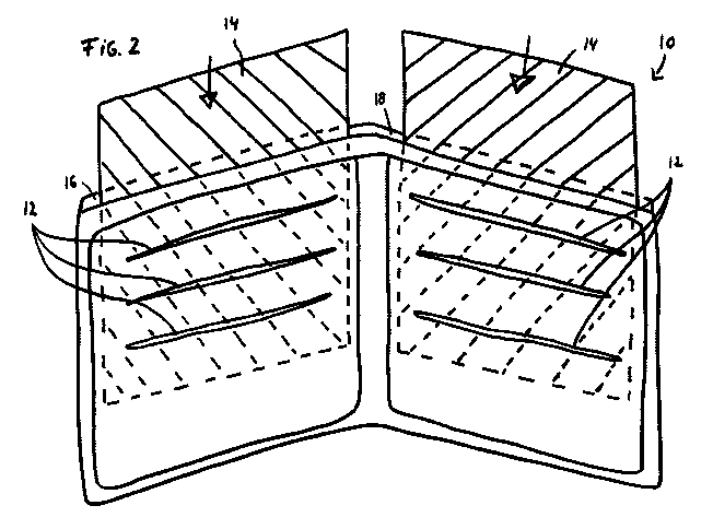
Figure 1 shows a conventional wallet 10 with six inside pockets 12 for
objects, for example
credit cards, Maestro cards, money cards, access cards for buildings or car
parks, driver's
license, identification card or similar cards that can be equipped with an
RFID or NFC chip. In
the open state of the wallet 10, that is shown in Figure 1, the inside pockets
12 are directly
accessible to a user. Behind the inside pockets 12, i.e. in the closed state
inclosing the inside
pockets from the outside, two surfaces 16, 18 are defined.
Figure 2 shows the wallet 10 from Figure 1 in a preferred embodiment of the
present
invention. According to the latter an electrically conductive layer in the
form of two
protective elements 14, which are examples of electrically conductive, two-
dimensional
objects, are each arranged on the two surfaces 16, 18 so that the inside
pockets 12 and the
cards located within them are shielded from the outside from electromagnetic
radio waves
by the surfaces 16, 18 when the wallet is closed. Instead of the protective
elements 14
shown in Figure 2, other at least partially electrically conductive objects
can also be used
that can preferably be made to be elastic. One example that works well is
graphite.
The protective elements 14 preferably have a film onto which, depending on the
application,
one or more layers of different materials, each with different conductivity,
permeability and
permittivity, can be vapor deposited. The layer thickness and the sequence of
materials
changes the electromagnetic properties of the end product. The resulting
effect is that
specific frequency bands can be specifically dampened. It is thus possible,
for example, to
effectively shield electromagnetic radiation in the megahertz range, while
those in the
kilohertz range can penetrate through the protective elements 14. Thus, the
reading out of
NFC elements, that are generally read out at a frequency of 13.56 MHz, can be
prevented,
while RFID tags, the working frequency of which is in the kilohertz range,
continue to
function.
In a particularly preferred embodiment a 35 nm to 50 nm, preferably 40 nm
thick aluminum
layer is vapor-deposited onto a film, a polyester layer of largely any
thickness is applied to
the latter, then another 35 nm to 50 nm, preferably 40 nm thick aluminum layer
is vapor
deposited, another polyester layer of largely any thickness is applied to the
latter, and
another 35 nm to 50 nm, preferably 40 nm thick aluminum layer is vapor-
deposited onto the
latter. The protective element 14 thus preferably has three aluminum layers,
each with a
thickness of 35 nm to 50 nm, preferably 40 nm, that are separated from one
another in each
instance by a polyester layer. An additional layer, for example a polyester
layer, is applied to
the outermost aluminum layer or to the outermost aluminum layers in order to
protect the
aluminum. Furthermore, it is possible to additionally provide a graphite layer
on which in
CA 02945546 2016-10-12
particular an RFID antenna or an entire RFID chip can be disposed which is
electrically
separated from the aluminum layers by the graphite due to its anisotropy.
Within this
context the anisotropy of the graphite means that a graphite layer
electrically conducts
along the individual layers of the graphite, whereas it insulates electrically
perpendicular to
its individual layers. This graphite layer is preferably at least 150 im
thick.
In total, this preferably produces an accumulated layer thickness of aluminum
or of some
other conductive material of between 70 nm and 200 nm, particularly preferably
of between
100 nm and 15 nm.
In an alternative preferred embodiment an aluminum layer that is between 35 nm
and 100
nm, preferably 50 nm thick, is respectively applied to both sides of a
polyester layer.
The protective element 14 should preferably have an overall thickness of
between 80 urn
and 150 nes so that it is easy to handle.
In Figure 2 the protective elements 14 are shown pushed two thirds of the way
into the
wallet 10 in order to make the protective elements 14 more visible. Provision
is made for the
finished embodiment such that the protective elements 14 are pushed fully into
the wallet
so that protection of all of the cards located within the inside pockets 12 is
guaranteed.
Unlike the exemplary embodiment shown in Figure 2, it is for example also
possible for a
protective element 14 to be made on one piece. Alternatively or additionally,
it is also
conceivable for protective elements to be applied to the wallet from the
outside, for
example adhered, stitched, vapor-deposited or fastened in some other way.
Alternatively,
electrically conductive dyes or materials can be vapor-deposited or printed.
In a preferred embodiment the protective element 14 comprises a plastic base
layer, on top
of this aluminum or copper film, and on top of this a graphite layer, the
sequence of these
layers also being able to be varied.
As an alternative to the wallet that is illustrated, the receptacle can be of
any other form.