Note: Descriptions are shown in the official language in which they were submitted.
POWER SUPPLY CIRCUIT WITH ACTIVE UNDER-VOLTAGE PROTECTION
[0001]
TECHNICAL FIELD
[0002] This relates to power supplies, and more particularly to power
supplies that
provide for under-voltage protection.
BACKGROUND
[0003] Electronic power supplies, used in a variety of applications,
typically provide
a defined (often regulated) voltage to downstream components. Power supplies
are
used in most modern electronic and electric applications to allow circuits to
be
designed to operate at voltages that do not equal voltages provided by
existing power
sources (e.g. batteries; mains voltages; etc.).
[0004] Often power supplies are fused, and include over-current protection.
[0005] At the same time, the deleterious effects of under-voltage have been
recognized. In particular, under-voltage has been a recognized problem in
battery
powered devices and power applications, where under-voltage may cause
malfunctions in circuitry, and the loss of data stored in memory. Typically,
however,
under-voltage protection circuits are specific to a defined voltage source.
[0006] Accordingly, there remains a need for a generalized under-voltage
protection circuit and power supply.
1
CA 2945678 2018-01-18
SUMMARY
[0007] As disclosed, a power supply circuit includes a protection circuit
interconnected
with an input voltage to the power supply. The protection circuit includes a
detection
circuit to detect whether a magnitude of the input voltage is below a defined
threshold.
The detection circuit includes a plurality of detectors, each for detecting
for a defined
voltage waveform, whether its magnitude is below a defined threshold voltage
for that
defined voltage waveform. Logic interconnects the detection circuit to provide
a control
signal for inhibiting the power supply from providing the output voltage if
the input
voltage is below the defined threshold for the defined voltage waveform, as
detected
by the detection circuit.
[0008] According to an aspect, there is provided a power supply circuit
comprising a
primary power supply for providing an output voltage from an input voltage; a
protection circuit interconnected with the input voltage, the protection
circuit
comprising a detection circuit to detect whether a magnitude of the input
voltage is
below a defined threshold, the detection circuit comprising a plurality of
detectors each
for detecting for a defined voltage waveform, whether its magnitude is below a
defined
threshold voltage; and logic interconnected with the detection circuit to
provide a
control signal for inhibiting the primary power supply from providing the
output voltage
if the input voltage is below the defined threshold, as detected by the
detection circuit.
[0009] According to another aspect, there is provided a method of operating a
power
supply circuit comprising a primary power supply and an auxiliary power
supply, the
method comprising: receiving an input voltage; using at least one active
component
powered by the auxiliary power supply to detect for a plurality of defined
input voltage
waveforms, whether a measure of the input voltage is below a defined
threshold; and
providing from the at least one active component a control signal for
inhibiting a
primary power supply from providing the output voltage if the input voltage is
below the
threshold, as detected by the at least one active component.
2
CA 2945678 2018-01-18
CA 02945678 2016-10-13
WO 2015/157857 PCT/CA2015/050092
[0010] Other features will become apparent from the drawings in conjunction
with
the following description.
BRIEF DESCRIPTION OF THE DRAWINGS
[0011] In the figures which illustrate example embodiments,
[0012] FIG. 1 is a block diagram of a power supply, exemplary of an
embodiment of
the present invention;
[0013] FIG. 2 is a block diagram of an example detection circuit of the
power supply
of FIG. 1;
[0014] FIG. 3 illustrates example voltage waveforms that may be provided to
the
power supply of FIG. 1;
[0015] FIGS. 4A-4C are block diagrams of waveform specific detectors of the
detection circuit of FIG. 2; and
[0016] FIG. 5 is a flow chart performed by an alternate detection circuit.
DETAILED DESCRIPTION
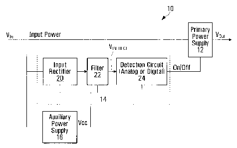
[0017] FIG. 1 is a schematic block diagram of an example power supply
circuit 10,
exemplary of an embodiment of the present invention. As illustrated, power
supply
circuit 10 includes a primary power supply 12, a protection circuit 14, and an
auxiliary
power supply 16.
[0018] Primary power supply 12 may be a conventional power supply circuit
and
may, for example, be an AC to DC supply, including a transformer rectifier and
filter
(all not shown) and optionally a voltage regulator (also not shown) to output
a defined
DC voltage. In alternate embodiments, primary power supply 12 could take the
form
of an AC power supply including the transformer and possibly a filter. Primary
power
3
supply 12 may also be a switched power supply or any other suitable power
supply
circuit. Primary power supply 12, however, relies on an input voltage VIN, to
produce
the defined Vow- Depending on the nature of primary power supply 12, the input
voltage may be an AC (sinusoid), DC or modified sine waveform voltage, or
other
waveform. Optionally, primary power supply 12 may be capable of operating with
a
multitude of source voltages having one of several different characteristic
waveforms.
Example voltage waveforms (VIN_DC, VIN_AC and VIN_MOD_SINE) that may be
provided as
VIN to provide to primary power supply 12 are depicted in FIG. 3A-C.
[0019] In particular, FIG. 3A depicts a time domain plot of a conventional DC
input.
FIG. 3B depicts a time domain plot of a standard AC (sine wave) input. FIG. 3C
depicts a time-domain plot of a "modified sine wave". As will be appreciated,
a
modified sine wave is a periodic waveform typically produced by a switching
power
supply and has three different output levels: a maximum, a minimum, and an
intermediate value between the maximum and the minimum. The modified sine wave
cycles between the maximum and minimum values once per cycle, like a square
wave. However, unlike a square wave which transitions between maximum and
minimum values nearly instantaneously, a modified sine wave spends some finite
duration at its intermediate value before transitioning to the next peak
value. The
intermediate value is typically zero, and the maximum and minimum values are
of
equal amplitude, and within each cycle the duration spent at the maximum and
minimum value is the same. The output levels, frequency, and duty cycle of a
modified
sine wave may be chosen so as to provide an approximation of a particular
sinusoid
suitable for a chosen application. For example, the parameters may be
chosen to provide identical peak voltage and RMS voltage to a particular
sinusoid.
[0020] In order to provide an output voltage of the desired magnitude VOUT,
the
magnitude of the input voltage, VIN must exceed some value VSAFE. In the
presence of
an input voltage below this value (an under-voltage) primary power supply 12,
unless
protected, may not function properly and may ultimately be damaged or damage
4
CA 2945678 2018-01-18
CA 02945678 2016-10-13
WO 2015/157857 PCT/CA2015/050092
downstream circuitry. As will be appreciated, VSAFE may differ depending on
the
characteristic waveform of the input voltage.
[0021] As such, primary power supply 12 may be prevented from switching ON
if
the input voltage is less than VSAFE. Likewise, once primary power supply is
ON, if the
input voltage drops below VSAFE, primary power supply 12 may be turned OFF.
[0022] As will be appreciated, in order to prevent primary power supply 12
from
oscillating between ON and OFF states, a threshold voltage VTIHRESHOLD_ON and
VTHRESHOLD_OFF may be chosen above and below at which primary power supply 12
will
turn ON and OFF, respectively, with VSAFEWTHRESHOLD_ON>VTHRESHOLD_OFF. This
may
ensure that primary power supply 12 does not turn ON and OFF continuously if
the
input voltage is too close to VTHRESHOLD_ON=
[0023] As noted, VSAFE may have different values depending on the nature of
the
input waveform. Likewise VTFIRESHOLD_ON and VTHRESHOLD_OFF may be chosen in
dependence on the waveform of VIN
[0024] Power supply circuit 10 further includes protection circuit 14 which
may
include an input rectifier 20, filter 22 and an under-voltage detection
circuit 24.
Protection circuit 14 includes active components ¨ analog or digital - capable
of
detecting under-voltage for a number of different input voltage waveforms.
[0025] An auxiliary power supply 16 powers protection circuit 14 and in
particular
the active components of protection circuit 14. Auxiliary power supply 16 may
be a
low voltage power supply, capable of operating at input voltages lower than
VTHREsHom_oN and VTHRESHOLD_OFF to provide an output voltage Vcc, and may, for
example, take the form of a switching power supply capable of being powered by
any
suitable input voltage waveform providing a relatively low operating voltage
Vcc to
protection circuit 14 (e.g. 3, 5 or even 12 volts). The operating voltage
provided by
auxiliary power supply 16 is typically significantly lower than VoLIT,
provided by primary
CA 02945678 2016-10-13
WO 2015/157857 PCT/CA2015/050092
power supply 12. Primary power supply 12 therefore suffers from an under-
voltage
condition well before auxiliary power supply 16.
[0026] Input rectifier 20 may take the form of a conventional full-wave
rectifier
formed, for example, by four diodes connected back to back. Filter 22 may
remove
high frequency noise from the rectified output provided by input rectifier 20.
Filter 22
may, for example, be formed as a plurality of capacitors, a digital filter or
the like. The
output of filter 22, VIN_RECT, is provided to detection circuit 24.
[0027] Detection circuit 24 is further detailed in FIGS. 2 and 4A-4C. In
particular, as
illustrated in FIG. 2, detection circuit 24 may include multiple waveform
detectors 26a,
26b, 26c (individually and collectively waveform detectors 26) that feed an OR-
gate
28.
[0028] Waveform detectors 26 may operate in parallel in order to detect the
nature
of the input voltage provided to a detector 26, as well as a measure of its
magnitude,
and in particular, to assess if its magnitude is less than some defined
threshold.
[0029] Example analog waveform detectors are schematically illustrated in
FIGS.
4A - 4C. FIG. 4A depicts a suitable waveform detector 26a for detecting a DC
voltage
(e.g. VIN DC Of FIG. 3). FIG. 4B depicts a suitable waveform detector 26b for
detecting
an AC (e.g. sinusoidal) waveform (e.g. VIN AC of FIG. 3). FIG. 4C illustrates
a detector
26c for detecting a modified sinewaveform (e.g. (VIN_MOD_SINE Of FIG. 3).
Optionally,
protection circuit 14 could include additional waveform detectors, for other
supported
input voltage waveform types.
[0030] As illustrated in FIG. 4A a DC waveform detector 26a includes two
comparators U1A and U1 B. Comparator U1A compares the input voltage as
filtered
by filter 22 to produce VIN_RECT, to a threshold voltage VIA, presented at the
non-
inverting input of comparator U1A. R1 and C1 further filter the input to U1A.
VIA is
initially established by R2 and R3 and VREFI as VTHRESHOLD_ON_DC. VREF may be
provided by a regulated source, such as a regulator powered by auxiliary power
supply
6
CA 02945678 2016-10-13
WO 2015/157857
PCT/CA2015/050092
16. If the input voltage VIN_RECT is less than this threshold, the output of
comparator
U1A will become low, outputting the saturation voltage of comparator U1A and
discharging capacitor 02, through resistor R7. The output of comparator U1B
remains
ON (high) provided that the voltage of capacitor 02 remains lower than a
second
threshold voltage VIE (established by R8 and R9) presented at the non-
inverting input
of comparator U1B, thus charging capacitor 03 through resistor R12 and diode
D2.
Diode D1 prevents capacitor 02 from discharging into comparator U1A. Likewise,
diode D2 prevents capacitor 03 from discharging into comparator U1B. V1E3 may
be
chosen in dependence on the saturation voltage of comparator U1B. Now, while
the
output of comparator U1B is high, transistor switch Q1 is turned ON,
effectively
connecting R4 to ground, in parallel with R3. R4 may be chosen so that VIA of
U1A
decreases to VTHRESHOLD_OFF_DC, thereby requiring the input voltage VIN_RECT
to drop
below VTHRESHOLD_OFF_DC for the output of comparator U1A to again become high,
thereby turning OFF Ql= VTRRESROI-D_ON_DC and VTHRESHOLD_OFF_Dc may be
empirically
determined for suitable threshold ON and OFF voltages for VIN, when VIN is a
constant
DC voltage (i.e. DC waveform). R4, R5, R6, R10, R11 and R14 are typical
biasing
resistors used as in conventional comparator circuits.
[0031] As
illustrated in FIG. 4B an AC waveform detector 26b also includes two
comparators U2A and U2B. Comparator U2A again compares the input voltage, as
filtered by filter 22 to a threshold voltage V2A presented at the non-
inverting input of
comparator U2A. R21 and 021 further filter the input to U2A. V2A is initially
established by R22 and R23 and VREF, as VTHRESHOLD_ON_AC. VREF may be the same
VREF provided to waveform detector 26a, such as a regulator powered by
auxiliary
power supply 16. If the input voltage to comparator U2A is less than this
threshold,
the output of comparator U2A will become low, outputting the saturation
voltage of
comparator U2A and discharging capacitor C22, through diode D21. Resistor R27
and capacitor C22 are chosen so that their RC constant is relatively high,
requiring the
input to U2A, VIN_RECT, to be below VTHRESHOLD_ON_AC for some time before
charging ¨
thereby filtering small dips in VIN_RECT. The output of comparator U2B remains
ON
(high) provided that the voltage of capacitor 022 remains lower than a second
7
CA 02945678 2016-10-13
WO 2015/157857 PCT/CA2015/050092
threshold voltage V23 (established by R28 and R29) presented at the non-
inverting
input of comparator U2B, thus charging capacitor 023 through resistor R32 and
diode
022. Diode D21 and resistor R27 allow capacitor C22 to discharge quickly into
comparator U2A as U2A provides a low output (signifying VIN_REcT >
VTHRESHOLD).
Diode 022 prevents capacitor 023 from discharging into comparator U2B. V2B may
be
chosen in dependence on the saturation voltage of comparator U2A. Again, while
the
output of comparator U2B is high, transistor switch Q2 is turned ON
effectively
connecting R24 to ground, in parallel with R23. R24 may be chosen so that if
V2A of
U2A decreases to VTHRESHOLD_OFF_AC, thereby requiring the input voltage
VIN_REcT to
drop below VTHRESHOLD_OFF_Ao for the output of comparator U2A to again become
low,
thereby turning OFF 02. Again, VTHRESHOLD_ON_AC and VTFIRESHOLD_OFF_AC may be
empirically determined for suitable threshold ON and OFF voltages for VIN,
when VIN is
a sinusoidal AC waveform. R24, R25, R26, R30, R31 and R34 are typical biasing
resistors used as in conventional comparator circuits.
[0032] As illustrated in FIG. 4C a modified sine waveform detector 26c
includes two
comparators U3A and U3B. Waveform detector 26c is well suited to detecting
threshold voltages in a non-sinusoidal voltage waveform (e.g. a modified sine-
wave
waveform as depicted in FIG. ). Comparator U3A again compares the input
voltage as
filtered by filter 22, VIN_RECT, to a threshold V3A presented at the non-
inverting input of
comparator U3A. R41 and 041 further filter the input to U3A. V3A is initially
established by R42 and R43 and VREF, as VTHRESHOLD_ON_MOD. VREF may again be
the
same VREF provided to waveform detectors 26a and 26b (such as by a regulator
powered by auxiliary power supply 16). If the input voltage to comparator U3A
is
greater than this threshold, the output of comparator U3A will become low,
discharging
capacitor C42, through resistor R47A and diode D41. Capacitor C42 and R47 are
chosen so that their RC constant is relatively high, allowing the input to
U3A, VIN_RECT,
to be below VTHRESHOLD for some time before discharging ¨ thereby filtering
the off
cycle in VIN_RECT= The output of comparator U3B remains ON (high) provided
that the
voltage of capacitor 042 remains lower than a second threshold voltage V3B
(established by R48 and R49) presented at the non-inverting input of
comparator U3B,
8
CA 02945678 2016-10-13
WO 2015/157857 PCT/CA2015/050092
thus charging capacitor C43 through resistor R52 and diode D32. Diode D41 and
resistor R47 and R47A allow capacitor C42 to discharge quickly into comparator
U3A
as comparator U3A provides a low output (signifying VIN_RECT > VTHRESHOLD).
Likewise,
diode D32 prevents capacitor 043 from discharging into comparator U38. V3B may
be
chosen in dependence on the saturation voltage of comparator U3A. Again, while
the
output of comparator U3B is high, transistor switch Q3 is turned ON
effectively
connecting R44 to ground, in parallel with R43. R44 may be chosen so that V3A
of
U3A decreases to VTHRESHOLD OFF MOD, thereby requiring the input voltage
VIN_RECT to
drop below VTHRESHOLD OFF MOD for the output of comparator U3A to again become
low,
thereby turning OFF Q3. Once again, VTHRESHOLD_ON_MOD and VTHRESHOLD_OFF_MOD
may
be empirically determined for suitable threshold ON and OFF voltages for
VIN_RECT,
when VIN RECT is a modified sine waveform. R44, R45, R46, R50, R51 and R54 are
typical biasing resistors used as in conventional comparator circuits.
[0033] The outputs of detectors 26a, 26b and 26c are provided to logic ¨ in
the
depicted embodiment in the form of a wired OR-gate 28 (FIG. 2). The output of
OR-
gate 28 then provides a control signal that enables or inhibits primary power
supply 12.
In particular, if none of detectors 26a, 26b, and 26c detect an input voltage
having
suitable magnitude (i.e. VIN<VTHRESHOLD ON DC OR VIN<VTHRESHOLD ON AC OR
VIN<VTHRESHOLD_ON_MOD) or, in steady state, if this measure drops below the
threshold
for a material time interval (i.e. VIN<VTHRESHOLD OFF_ DC OR VIN<VTHRESHOLD
OFF AC OR
VIN<VTHRESHOLD_OFF_MOD), primary power supply 12 is disabled and no power is
output
by circuit 10. In this way, primary power supply 12, as well as downstream
components powered by primary power supply 12 may be protected from under-
voltage.
[0034] In an alternate embodiment, detection circuit 24 may be formed as a
digital
processing circuit, embodied in a digital signal processor (DSP), application
specific
integrated circuit (ASIC), general purpose processor, or the like. So
implemented,
circuit 24 may be suitably programmed with, for example, processor executable
9
CA 02945678 2016-10-13
WO 2015/157857 PCT/CA2015/050092
instructions stored in processor readable memory, to perform blocks S400 set
forth in
FIG. 5, performing generally similar to detectors 26a, 26b and 26c.
[0035] As illustrated, input voltage VIN_RECT is digitized in block S402.
The nature of
the input voltage is detected in blocks S404-S408. In particular, a DC voltage
waveform is detected from the digitized voltage in block S404. If, the voltage
is DC,
blocks S410-S416 are performed (similar to detector 26a).
[0036] If the input voltage VIN_RECT is not assessed to be DC waveform, the
digitized signal is processed in block S406 to assess if it is an AC
(sinusoidal) voltage,
or a modified sine waveform. If, for example, the input voltage waveform has a
predetermined number of peaks, it may be assessed to be an AC voltage waveform
in
block S408, and blocks S420-S426 may be performed (similar to detector 26b).
If not,
the voltage may be assessed to be a modified sine waveform and blocks S430-
S436
may be performed (similar to detector 26c).
[0037] If the waveform is a DC voltage, a determination is made if the
sampled DC
voltage exceeds a threshold voltage Val in block S410. If so, a power supply
enable
signal may be output in block S412, enabling primary power supply 12. The
signal
remains ON, as long as the VIN_RECT remains greater than a second threshold
voltage
Va2, as determined in block S414. If VIN_RECT falls below the second threshold
voltage
V52, the primary power supply enable signal may be inhibited in block S416,
turning
OFF primary supply 12.
[0038] Similarly, if the waveform is an AC (sinusoidal) voltage, a
determination is
made if the sampled AC voltage exceeds a threshold voltage Vbi in block S420.
If so,
a primary power supply enable signal may be output in block S422. The signal
remains ON, as long as the VIN_REcT remains greater than a second threshold
voltage
Vb2, as determined in block S424. If VIN_RECT falls below the second threshold
voltage
Vb2, the primary power supply enable signal may be inhibited in block S426,
turning
OFF primary supply 12.
CA 02945678 2016-10-13
WO 2015/157857 PCT/CA2015/050092
[0039] Likewise, if the waveform is a modified sine waveform voltage, a
determination is made if the sampled wave voltage exceeds a threshold voltage
Vi in
block S430, if so a primary power supply enable signal may be output in block
S432.
The signal remains ON, as long as the VIN_RECT remains greater than a second
threshold voltage Vc2, as determined in block S434. If VIN_REcT falls below
the second
threshold voltage Vc2, the primary power supply enable signal may be inhibited
in block
S436, thus also inhibiting primary power supply 12.
[0040] As will be appreciated, the threshold voltages detected will depend
on the
detection method/circuit used, and the nature of the input voltage waveform.
[0041] Conveniently then, detection circuit 24 is able to detect a variety
of input
voltage waveforms to ensure that they can provide an input voltage, that over
time,
allow for proper operation of primary power supply 12, preventing malfunction
and/or
damage resulting to power supply 12, or downstream components from under-
voltage.
As will be appreciated, other detectors could be added to detection circuit,
to detect
other applied voltage waveforms.
[0042] Of course, the above described embodiments are intended to be
illustrative
only and in no way limiting. The described embodiments are susceptible to many
modifications of form, arrangement of parts, details, and order of operation.
The
invention, rather, is defined by the appended claims.
11