Note: Descriptions are shown in the official language in which they were submitted.
CA 02946226 2016-10-20
SCALABLE PLANAR PACKAGING ARCHITECTURE FOR ACTIVELY SCANNED
PHASED ARRAY ANTENNA SYSTEM
BACKGROUND
In the field of phased array antennas, there is an ongoing effort to provide
an
affordable high fidelity phased array subarray tile assembly for use as a
building
block in phased array antennas. Typically, phased array antenna systems (e.g.,
subarray tile assemblies) are designed and manufactured in large array
configurations to meet particular applications. Such systems are complex
requiring
many parts and many hours to fabricate, assemble, and test the end product.
Furthermore, larger and more complex assemblies are difficult to manufacture
adding to higher costs due to lower yields.
Conventional techniques employed for providing phased array antennas tend
to be single point solutions for particular applications. As such, these
products are,
for the most part, expensive and less adaptable. For example, existing
solutions for
providing a lower cost high fidelity antenna array often rely on integrating
more
functionality into larger array tile assemblies. However, larger array tile
assemblies
add complexity to printed wiring boards in multiple laminations, thicker
overall board
dimensions, higher via-aspect ratios, and large number of vias resulting in
lower-
yield of manufactured assemblies and higher cost.
Accordingly, there is a need for an improved phased array antenna
implementation that provides high fidelity phased array antenna performance
without
excessive cost.
SUMMARY
One or more examples relate generally to phased array antennas and, more
particularly to scalable planar phased array antenna subarray tile assemblies.
Systems and methods are disclosed herein in accordance with one or more
1
CA 02946226 2016-10-20
examples that provide an improved approach to providing a scalable planar
phased
array antenna subarray tile assembly. In some examples, a subarray tile
assembly is
implemented as a printed wiring board (PWB) with antenna elements coupled to
the
PWB. In one example, a PWB may include integrated circuit die attached
directly to
the PWB and coupled to the antenna elements. A single integrated circuit die
may
include four beamforming circuits and couple to four antenna elements to
perform
beamforming operations. The integrated circuit die is coupled to the antenna
elements through conductive vias formed in the PWB. Microvias formed in PWB
layers couple to the integrated circuit die. The microvias are coupled to
larger plated
through hole vias, where the plated through hole vias are offset to provide a
thermal
mechanical stress relief to the integrated circuit die. The plated through
hole vias
extend through layers of the PWB and are coupled to the antenna elements.
In one example, a system includes a phased array antenna subarray tile
assembly comprising a printed wiring board (PWB) comprising a plurality of
layers;
an integrated circuit die coupled to a first surface of the PWB; an antenna
element
coupled to a second surface of the PWB; a first conductive via having a first
diameter, the first conductive via being coupled to the integrated circuit die
and
extending through a first subset of the layers; a second conductive via having
a
second diameter larger than the first diameter, the second conductive via
being
offset from the first conductive via, extending through a second subset of the
layers,
and being coupled to the antenna element; a conductive trace of the PWB
coupled
to the first and second conductive vias; and wherein the offset of the second
conductive via provides a thermal mechanical stress relief to the integrated
circuit
die.
In another example, a system includes a subarray tile assembly comprising a
substantially planar printed wiring board (PWB) comprising a plurality of
layers; one
or more integrated circuit die coupled to a first surface of the PWB; at least
four
antenna elements coupled to a second surface of the PWB, wherein the at least
four
antenna elements are arranged in a square lattice grid on the PWB; and wherein
the
2
integrated circuit die is electrically coupled to each of the four antenna
elements
through the layers and wherein the offset of the second conductive via
provides a
thermal mechanical stress relief to the integrated circuit die .
In another example, a method includes passing an RF signal along a
conductive path through a printed wiring board (PWB) between an integrated
circuit
die and an antenna element, wherein the conductive path comprises: a first
conductive
via having a first diameter, the first conductive via being coupled to the
integrated
circuit die and extending through a first subset of layers of the PWB; a
second
conductive via having a second diameter larger than the first diameter, the
second
conductive via being offset from the first conductive via, extending through a
second
subset of layers of the PWB, and being coupled to the antenna element such
that the
offset of the second conductive via provides a thermal mechanical stress
relief to the
integrated circuit die; and a conductive trace of the PWB coupled to the first
and
second conductive vias.
In another example, a method of forming a phased array antenna subarray tile
assembly includes providing a printed wiring board (PWB) comprising a
plurality of
layers; providing an integrated circuit die coupled to a first surface of the
PWB;
providing an antenna element coupled to a second surface of the PWB;
electrically
coupling the integrated circuit die to a first conductive via extending
through a first
subset of the layers; and electrically coupling the first conductive via to a
second
conductive via offset from the first conductive via, extending through a
second subset
of the layers, and coupled to the antenna element, wherein the offset of the
second
conductive via provides a thermal mechanical stress relief to the integrated
circuit die.
In another example, a method described above includes providing a metallic
honeycomb structure comprising a plurality of cylindrical waveguides
configured to
interface with a plurality of the phased array antenna subarray tile
assemblies; forming
a recess along a surface of each of the cylindrical waveguides; filling the
cylindrical
waveguides and the recesses with a dielectric material; and wherein each
filled recess
mechanically secures the dielectric material to the cylindrical waveguide.
3
Date Recue/Date Received 2020-10-21
In one embodiment, there is provided a phased array antenna subarray tile
assembly. The assembly includes a printed wiring board "PWB" including a
plurality
of layers, an integrated circuit die coupled to a first surface of the PWB, an
antenna
3a
Date Recue/Date Received 2020-10-21
element coupled to a second surface of the PWB, a first conductive via having
a first
diameter. The first conductive via is coupled to the integrated circuit die
and extends
through a first subset of the layers, a second conductive via having a second
diameter larger than the first diameter, the second conductive via being
offset from
the first conductive via, extending through a second subset of the layers, and
being
coupled to the antenna element; a conductive trace of the PWB coupled to the
first
and second conductive vias; and wherein the offset of the second conductive
via
provides a thermal mechanical stress relief to the integrated circuit die.
The integrated circuit die may be a flip chip including a plurality of solder
bumps coupled to the first surface of the PWB, and at least one of the solder
bumps
may be electrically coupled to the first conductive via.
The system may include an interposer printed wiring board "PWB", wherein
the integrated circuit die may be a flip chip including a plurality of solder
bumps
coupled to a first surface of the interposer PWB. A second surface of the
interposer
PWB may include a ball grid array coupled to the first surface of the PWB, and
at
least one of the balls may be electrically coupled to the first conductive
via.
The integrated circuit die may be configured to provide a polarized radio
frequency "RE" signal passed to the antenna element through the first and
second
conductive vias.
The system may include a plurality of the antenna elements, a plurality of the
first and second conductive vias, and the integrated circuit die may be
configured to
provide the corresponding polarized RF signal passed to each of the antenna
elements through corresponding ones of the first and second conductive vias.
The system may include a built-in test circuit formed within the integrated
circuit die; a controller coupled to the built-in test circuit. The built-in
test circuit may
be configured to provide a first test signal to the integrated circuit die and
receive a
second test signal from the integrated circuit die; and the controller may
receive the
second test signal to compare to a reference second test signal.
4
CA 2946226 2020-01-17
The system may include an in-flight calibration circuit formed within the
integrated circuit die; and the in-flight calibration circuit may be
configured to adjust
an operation of the system in response to a signal received through the first
conductive via.
The antenna element may be configured to provide an RF signal passed to
the integrated circuit die through the second and first conductive vias, and
the
integrated circuit die may be configured to convert the RF signal provided by
the
antenna element to a polarized RF signal.
The system may include a plurality of antenna elements, a plurality of first
and
second conductive vias, wherein each antenna element may be configured to
provide an RF signal passed to the integrated circuit die through
corresponding ones
of the second and first conductive vias; and the integrated circuit die may be
configured to convert the RF signal provided by each antenna element to a
polarized
RF signal.
The system may include a metallic honeycomb structure, a plurality of
cylindrical waveguides formed within the metallic honeycomb structure. Each
cylindrical waveguide may have a radius that is substantially equal to a
radius of a
corresponding antenna element; a recess at an intermediate position formed
along a
surface of each of the cylindrical waveguides. The cylindrical waveguides and
the
recesses may be filled with a dielectric material, and each filled recess may
mechanically secure the dielectric material to the cylindrical waveguide.
The dielectric material may have a coefficient of thermal expansion "CTE"
substantially equal to a CTE of the metallic honeycomb structure; and the
dielectric
material may have a dielectric constant substantially equal to a dielectric
constant of
the PWB.
The system may include a plurality of wide angle impedance match "WAIM"
layers of material disposed on an exposed surface of the plurality of
cylindrical
waveguides and an outer surface of the metallic honeycomb structure.
The metallic honeycomb structure may include aluminum.
5
CA 2946226 2020-01-17
The system may include an RF distribution circuit formed on at least one of
the second subset of the layers, a plurality of ground vias extending through
the
second subset of the layers. The plurality of ground vias may be distributed
about a
perimeter around the second conductive via to provide a waveguide cage around
the
second conductive via; and wherein the plurality of ground vias further reduce
radio
frequency interference "RFI" within the RF distribution circuit.
The system may include a plurality of phased array antenna subarray tile
assemblies, an aperture housing including a plurality of cylindrical
waveguides
coupled to the plurality of subarray tile assemblies, an array distribution
printed
wiring board "PWB" coupled to the plurality of subarray tile assemblies; and a
cold
plate disposed between the array distribution PWB and the plurality of
subarray tile
assemblies.
In another embodiment, there is provided a system. The system includes a
subarray tile assembly including a substantially planar printed wiring board
"PWB"
including a plurality of layers, one or more integrated circuit die coupled to
a first
surface of the PWB, at least four antenna elements coupled to a second surface
of
the PWB. The at least four antenna elements are arranged in a square lattice
grid
on the PWB; and wherein the integrated circuit die is electrically coupled to
each of
the four antenna elements through the layers.
The integrated circuit die may include a silicon germanium alloy.
The integrated circuit die may be configured to receive an RF signal from
each of the four antenna elements and convert the corresponding RF signal to a
polarized RF signal.
The system may include the first conductive via having a first diameter, and
the second conductive via having a second diameter larger than the first
diameter.
The offset of the second conductive via may provide a thermal mechanical
stress
relief to the integrated circuit die.
6
CA 2946226 2020-01-17
The integrated circuit die may be a flip chip including a plurality of solder
bumps coupled to the first surface of the PWB, and wherein at least one of the
solder bumps is electrically coupled to the first conductive via.
The system may include an RF distribution circuit formed on at least one of
the second subset of the layers, a plurality of ground vias extending through
the
second subset of the layers, the plurality of ground vias being distributed
about a
perimeter around the second conductive via to provide a waveguide cage around
the
second conductive via; and wherein the plurality of ground vias further reduce
radio
frequency interference "RFI" within the RF distribution circuit.
In another embodiment, there is provided a method. The method involves
passing an RF signal along a conductive path through a printed wiring board
"PWB"
between an integrated circuit die and an antenna element. The conductive path
may
include a first conductive via having a first diameter. The first conductive
via is
coupled to the integrated circuit die and extending through a first subset of
layers of
the PWB, a second conductive via having a second diameter larger than the
first
diameter. The second conductive via is offset from the first conductive via,
extending through a second subset of layers of the PWB, and is coupled to the
antenna element, and a conductive trace of the PWB coupled to the first and
second
conductive vias.
The integrated circuit die may be configured to provide a polarized radio
frequency "RE" signal passed to the antenna element through the first and
second
conductive vias.
The method may involve a plurality of the antenna elements, a plurality of the
first and second conductive vias; and the integrated circuit die may be
configured to
provide a corresponding polarized RF signal passed to each of the antenna
elements through corresponding ones of the first and second conductive vias.
The antenna element may be configured to provide a radio frequency "RE"
signal passed to the integrated circuit die through the second and first
conductive
7
CA 2946226 2020-01-17
vias, and wherein the integrated circuit die may be configured to convert the
RF
signal provided by the antenna element to a polarized RF signal.
The method may involve a plurality of the antenna elements; a plurality of the
first and second conductive vias; and each antenna element may be configured
to
provide an RF signal passed to the integrated circuit die through
corresponding ones
of the second and first conductive vias, and the integrated circuit die may be
configured to convert the RF signal provided by each antenna element to a
polarized
RF signal.
In another embodiment, there is provided a method of forming a phased array
antenna subarray tile assembly. The method involves providing a printed wiring
board "PWB" including a plurality of layers, providing an integrated circuit
die
coupled to a first surface of the PWB, providing an antenna element coupled to
a
second surface of the PWB. The method further invovles electrically coupling
by a
conductive trace of the PWB the integrated circuit die to a first conductive
via
extending through a first subset of the layers; and electrically coupling the
first
conductive via to a second conductive via offset from the first conductive
via,
extending through a second subset of the layers, and coupled to the antenna
element.
Providing the integrated circuit die may involve coupling a plurality of
solder
bumps configured on a first surface of the integrated circuit die to the first
surface of
the PWB, wherein at least one of the solder bumps is electrically coupled to
the first
conductive via; and underfilling an area between the integrated circuit die
first
surface and the first surface of the PWB.
Providing the integrated circuit die may involve coupling a plurality of
solder
bumps configured on a first surface of the integrated circuit die to a first
surface of an
interposer printed wiring board "PWB", underfilling an area between the first
surface
of the integrated circuit die and the first surface of the interposer PWB; and
coupling
a ball grid array "BGA" configured on a second surface of the interposer PWB
to the
first surface of the PWB, wherein at least one of the balls in the BGA is
electrically
coupled to the first conductive via.
8
CA 2946226 2020-01-17
The method may involve providing a metallic honeycomb structure, forming a
plurality of cylindrical waveguides within the metallic honeycomb structure,
wherein
each cylindrical waveguide has a radius that is substantially equal to a
radius of a
corresponding antenna element, forming a recess at an intermediate position
along
a surface of each of the cylindrical waveguides, filing the cylindrical
waveguides and
the recesses with a dielectric material, the dielectric material having a
dielectric
constant that is substantially equal to a dielectric constant of the PWB; and
wherein
each filled recess mechanically secures the dielectric material to the
cylindrical
waveguide.
The method may involve forming an RE distribution circuit on at least one of
the second subset of the layers; forming a plurality of ground vies extending
through
the second subset of the layers. The plurality of ground vies may be
distributed
about a perimeter around the second conductive via to provide a waveguide cage
around the second conductive via; and wherein the plurality of ground vies
further
reduce radio frequency interference "RFI" within the RF distribution circuit.
In another embodiment, there is provided a further method. The method
involves
providing a metallic honeycomb structure comprising a plurality of
cylindrical waveguides configured to interface with a plurality of the phased
array
antenna subarray tile assemblies. The method further involves forming a recess
at
an intermediate position along a surface of each of the cylindrical
waveguides; filling
the cylindrical waveguides and the recesses with a dielectric material; and
wherein
each filled recess mechanically secures the dielectric material to the
cylindrical
waveguide.
The metallic honeycomb structure may include aluminum.
The method may involve a plurality of antenna elements coupled to the
plurality of cylindrical waveguides, each cylindrical waveguide may have a
radius
that is substantially equal to a radius of a corresponding antenna element.
The dielectric material may contact the PWB of each of the subarray tile
assemblies, the filling the cylindrical waveguides may involve molding a
dielectric
9
CA 2946226 2020-01-17
material in a shape substantially corresponding to the cylindrical waveguide
and the
recesses. The dielectric material may have a coefficient of thermal expansion
"CTE"
substantially equal to a CTE of the metallic honeycomb structure, and the
dielectric
material may have a dielectric constant substantially equal to a dielectric
constant of
the PWB; and placing the molded dielectric material into each of the
cylindrical
waveguides to fill the cylindrical waveguides and the recesses.
The dielectric material may contact the PWB of each of the subarray tile
assemblies. The filling of the cylindrical waveguides may involve injecting
the
dielectric material into each of the cylindrical waveguides and recesses. The
dielectric material may have a coefficient of thermal expansion "CTE"
substantially
equal to a CTE of the metallic honeycomb structure, and the dielectric
material may
have a dielectric constant substantially equal to a dielectric constant of the
PWB.
A more complete understanding of examples of various embodiments will be
afforded to those skilled in the art, as well as a realization of additional
advantages
thereof, by a consideration of the following detailed description of one or
more
examples. Reference will be made to the appended sheets of drawings that will
first
be described briefly.
BRIEF DESCRIPTION OF THE DRAWINGS
Fig. 1 illustrates an external view of a phased array antenna system in
accordance with an example of the disclosure.
Fig. 2 illustrates an exploded view of a phased array antenna system in
accordance with an example of the disclosure.
CA 2946226 2020-01-17
CA 02946226 2016-10-20
Fig. 3 illustrates an exploded view of an antenna integrated printed wiring
board (AiPWB) interface to an array distribution printed wiring board (PWB) in
accordance with an example of the disclosure.
Fig. 4 illustrates a cross-section view of a phased array antenna system in
accordance with an example of the disclosure.
Fig. 5 illustrates a cross-section view of an AiPWB coupled to integrated
circuit die and a waveguide in accordance with an example of the disclosure.
Fig. 6 illustrates a cross-section view of an integrated circuit die
connection to
antenna elements through an AiPWB in accordance with an example of the
disclosure.
Fig. 7 illustrates a view of an AiPWB waveguide coupled to a cylindrical
waveguide in accordance with an example of the disclosure.
Fig. 8 illustrates a cross-section view of an AiPWB in accordance with an
example of the disclosure.
Fig. 9 illustrates a view of a RF distribution layer of an AiPWB in accordance
with an example of the disclosure.
Fig. 10A illustrates a view of a subarray tile assembly in accordance with an
example of the disclosure.
Fig. 10B illustrates a view of a transmit phased array antenna in accordance
with an example of the disclosure.
Fig. 10C illustrates a view of a receive phased array antenna in accordance
with an example of the disclosure.
Fig. 11A illustrates integrated circuit die connections to antenna elements in
accordance with an example of the disclosure.
11
CA 02946226 2016-10-20
Fig. 11B illustrates an exploded view of an integrated circuit die in
accordance
with an example of the disclosure.
Fig. 11C illustrates receive element electronics in accordance with an
example of the disclosure.
Fig. 11D illustrates transmit element electronics in accordance with an
example of the disclosure.
Fig. 12A illustrates a process of using a receive subarray tile assembly in
accordance with an example of the disclosure.
Fig. 12B illustrates a process of using a transmit subarray tile assembly in
accordance with an example of the disclosure.
Fig. 13 illustrates a process of providing a phased array antenna subarray
tile
assembly in accordance with an example of the disclosure.
DETAILED DESCRIPTION
Examples of the present disclosure provide for a scalable subarray tile
assembly that significantly reduces parts count, fabrication processing,
manufacturing/assembly steps and phase array antenna costs. As such, the
scalable
subarray tile assembly can be replicated in any planar direction to develop a
larger
integrated phased array aperture.
In some examples, an antenna integrated printed wiring board (AiPWB)
includes a first subset of thin pre-pegs/copper layers adjoining a first
surface (e.g., a
top surface) to accommodate a plurality of first conductive vias (e.g., laser
drilled
microvias). The first conductive vias are used for direct connection to high
density
integrated circuit die incorporating fine pitch ball grids. By utilizing thin
pre-
pegs/copper layers and laser drilled microvias on the first subset of layers,
the
AiPWB design can accommodate fine pitch integrated circuit die attached
directly to
12
CA 02946226 2016-10-20
a top surface and connected through the layers of the AiPWB. This allows for
increased electronic circuit packaging density not previously possible.
In some examples, the AiPWB includes a second subset of layers used, in
part, as a waveguide transition section. Included in the second subset of
layers are
second conductive vias (e.g., plated through vias) coupled to the first
conductive
vias, extending through the second subset of layers and coupled to antenna
elements on a second surface (e.g., a bottom surface). The second conductive
vias
are offset from the first conductive vias to provide a thermal and mechanical
stress
relief to the fine pitch integrated circuit die interconnect. Furthermore, the
first and
second conductive vias are coupled within the AiPWB by a conductive trace. In
this
regard, the fine pitch integrated circuit die directly attached to the top
surface of the
AiPWB is reliably coupled to the antenna element to provide for antenna
beamforming operations.
In some examples, the integrated circuit die is fabricated from a silicon
.. germanium (SiGe) alloy which requires less area for radio frequency (RF)
electronics
than conventional RE circuits, for example, such as gallium arsenide alloy. A
single
integrated circuit die contain element electronics to provide beamforming
operations
to four antenna elements. The area saved by using SiGe integrated circuit die
and
the ability to reliably connect the fine pitch ball grids to four antenna
elements
significantly reduces the area requirements on the lattice for electronics and
simplifies the assembly of the array. The reduction in area requirements
allows for
implementation of a square planar subarray tile assembly, for example, as a 64
antenna element subarray tile assembly (e.g., an eight by eight matrix).
In some examples, implementing the AiPWB as a square planar subarray tile
assembly allows for routing RE distribution circuits on the second subset of
layers
using the interstitial regions between the waveguides. Ground vias extending
through the waveguide transition section (e.g., a second subset of the layers)
are
distributed around each second conductive via coupled to the antenna element
to
form a waveguide cage. In this regard, twenty-four ground vies may be used for
13
CA 02946226 2016-10-20
each antenna element waveguide cage. The ground vias are re-used on the
transition section layers to reduce radio frequency interference within the RF
distribution circuit. By re-using ground vias, the AiPWB via count is
significantly
reduced (e.g., a tenfold reduction in vias) making for a less complex and cost
.. effective AiPWB.
In some examples, a metallic honeycomb structure is coupled to the AiPWB.
Cylindrical waveguides are formed within the metallic honeycomb structure and
are
coupled to the antenna elements. The waveguides may be filled with a
dielectric
material. The dielectric material may be chosen for properties that is low
loss at RF
frequencies and has the correct dielectric constant at RF frequencies. The
dielectric
material may be chosen to accommodate a lower waveguide cutoff frequency and a
smaller diameter of the antenna element. Furthermore, a dielectric material
may be
chosen for a coefficient of thermal expansion (CTE) to match the metallic
honeycomb. The dielectric material may be formed within the cylindrical
waveguide
opening using an injection molded or compression molded process. In some
examples, recesses are formed along surfaces of the cylindrical openings to
secure
the dielectric material in the waveguide.
In some examples, additional AiPWB layers may be used to provide built-in
test and in-flight calibration signals. Further, built-in test may be
integrated into the
SiGE integrated circuit to provide a self-test capability. The use of built-in
test and in-
flight calibration reduces the need for 100 percent test at the subarray tile
assembly
level while still maintaining a robust system test program translating into a
significant
cost savings.
In general, the AiPWB utilizes a more cost-effective subarray size (e.g., 64
elements arranged in an eight by eight matrix) in order to achieve a large
array size.
The subarray tile assembly is an integration of a variety of technologies to
increase
performance and functionality while reducing cost, size, weight and power of a
scalable building block that varies sub-array dimensions and footprint to
optimize
14
CA 02946226 2016-10-20
fabrication, assembly, manufacturability and test of the integrated phased
array
antenna.
In one example, a PWB may be provided that includes a plurality of integrated
circuit die and antenna elements. The integrated circuit die are coupled to
the
antenna elements by conductive vias extending through a plurality of layers of
the
PWB. A first conductive extending through a first subset of the layers is
coupled to
the integrated circuit die. A second conductive via extending through a second
subset of the layers is coupled to the antenna element. The second conductive
via is
offset from the first conductive via and coupled to the first conductive via
by a
conductive trace on a layer of the PWB.
In another example, a subarray tile assembly may be provided that includes a
substantially planar PWB and one or more integrated circuit die coupled to a
first
surface of the PWB. At least four antenna elements are arranged in a square
lattice
grid on a second surface of the PWB. A single integrated circuit die is
electrically
coupled to each of the four antenna elements through the layers of the PWB.
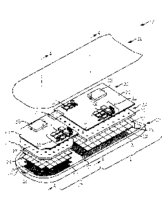
Fig. 1 illustrates an external view of a phased array antenna system 100 in
accordance with an example of the disclosure. Phase array antenna system 100
may be used to transmit and receive radio frequency (RF) communication or
radar
signals in accordance with various techniques described herein. Phased array
antenna system 100 may be used on a variety of platforms, such as a land
based,
an airplane, or a space based platform. Phased array antenna system 100
includes
a transmit antenna aperture 102 and a receive antenna aperture 103. In some
examples, transmit antenna aperture 102 may include two thousand forty-eight
transmit elements and receive antenna aperture may include two thousand six
hundred eighty-eight receive elements. Phased array antenna system 100 may
include an aperture housing 106 including one or more mounting flanges 108 to
securely mount phased array antenna system 100 to a platform such as, for
example, an airplane antenna fairing. Aperture housing 106 may include a
metallic
honeycomb structure 107 and a plurality of cylindrical waveguides 105 formed
within
CA 02946226 2016-10-20
metallic honeycomb structure 107. The metal of metallic honeycomb structure
107
may include aluminum in the form of pure aluminum or an aluminum alloy. In
some
examples, waveguides 105 may be configured as rectangular, square, or any
other
shape appropriate for a waveguide 105. Data and power feed through connectors
109 are provided for each of transmit antenna aperture 102 and receive antenna
aperture 103 to receive and transmit data, and receive power from external
sources.
In some examples, circular flange mount connectors 109 are provided, however,
other types of data and power connectors are possible. Coaxial RF feed through
connectors 119 are provided for each of transmit and receive antenna
apertures,
102 and 103. Phased array antenna system 100 may provide for a shared aperture
compact radar and communications antenna architecture that may provide
performance, size, and weight advantages.
Fig. 2 illustrates an exploded view of a phased array antenna system 100 in
accordance with an example of the disclosure. Phased array antenna system 100
may include an aperture assembly 201, an antenna array 202 including a receive
phased array antenna subsystem 211 and a transmit phased array antenna
subsystem 215, a cold plate assembly 204, an array distribution assembly 206,
and
a cover 208.
Aperture assembly 201 may include aperture housing 106 incorporating
metallic honeycomb structure 107 and the plurality of cylindrical waveguides
105
formed within metallic honeycomb structure 107, as described herein. In some
examples, cylindrical waveguides 105 may be filled with a dielectric material,
as
described herein. In some examples, dielectric material may be chosen to
accommodate performance improvements. For example, improvements in scanning
wide angles and increasing frequency bandwidth may require a dielectric
material
with properties to accommodate changes in waveguide cutoff frequency and
element
diameter associated with such improvements.
As shown in Fig. 2, antenna array 202 includes receive phased array antenna
214 and transmit phased array antenna 218. Each of receive phased array
antenna
16
CA 02946226 2016-10-20
214 and transmit phased array antenna 218 include a plurality of phased array
antenna subarray tile assemblies. In some examples, receive phased array
antenna
214 includes forty-two receive phased array antenna subarray tile assemblies
224.
In some examples, transmit phased array antenna 218 includes thirty-two
transmit
phased array antenna subarray tile assemblies 228. More or fewer subarray tile
assemblies are possible in other examples of receive phased array antenna 214
and
transmit phased array antenna 218. In this regard, the phased array subarray
tile
assembly (e.g., receive phased array antenna subarray tile assembly 224 and/or
transmit phased array antenna subarray tile assembly 228) forms a scalable
building
block for use in a large phased array antenna.
In the example shown in Fig. 2, a cold plate assembly 204 includes a receive
cold plate 213 and a transmit cold plate 217. Cold plate assembly 204 may be
configured to couple to antenna array 202 on a first surface and array
distribution
assembly 206 on a second surface. Cold plate assembly 204 may be configured to
maintain a safe operating temperature for each of the coupled antenna array
202
and array distribution assembly 206. In some examples, residual heat from
antenna
array 202 and/or array distribution assembly 206 may be passively transferred
to
cold plate assembly 204. In other examples, cold plate assembly 204 may be
formed
with channels to accept a fluid in order to actively cool antenna array 202
and/or
array distribution assembly 206. Receive cold plate 213 may be coupled to
receive
phased array antenna 214 on a first surface and a receive array distribution
printed
wiring board (PWB) 212 on a second surface. Transmit cold plate 217 may be
coupled to transmit phased array antenna 218 on a first surface and a transmit
array
distribution printed wiring board (PWB) 216 on a second surface. A plurality
of
openings 209 formed through receive cold plate 213 and transmit cold plate 217
may
accept connectors configured to provide an electrical interface between
antenna
array 202 and array distribution assembly 206, as described herein.
In the example shown in Fig. 2, phased array antenna system 100 includes
an array distribution assembly 206. Array distribution assembly 206 includes
receive
17
CA 02946226 2016-10-20
array distribution PWB 212 and transmit array distribution PWB 216 to provide
power, data, clocks, and/or control signals to antenna array 202. In this
regard,
power and control circuit 222 of receive array distribution MB 212 may provide
RF,
DC power, and control signals to each of receive subarray tile assemblies 224
of
receive phased array antenna 214.
Furthermore, power and control circuit 222 may provide a controller 230 to
interface with integrated circuit die of receive subarray tile assembly 224.
Controller
230 may include, for example, a microprocessor, a logic device (e.g., a
programmable logic device configured to perform processing operations), a
digital
signal processing (DSP) device, one or more memories for storing executable
instructions (e.g., software, firmware, or other instructions), and/or any
other
appropriate combination of processing device and/or memory to execute
instructions
to perform any of the various operations described herein.
Controller 230 of power and control circuit 222 may be coupled to a built-in
test circuit (e.g., such as built-in test circuit 1162 of Fig. 11) formed
within an
integrated circuit die (e.g., such as integrated circuit die 540 of Fig. 5).
In some
examples, built-in test circuit may provide test signals substantially similar
to system
signals. In this regard, the built-in test circuit may be configured to
provide a first test
signal (1101a through 1101c) to the integrated circuit die 540 and receive a
second
test signal (1102a through 1102d) from the integrated circuit die 540.
Controller 230
receives the second test signal to compare to a reference second test signal.
Furthermore, an in-flight calibration circuit (e.g., such as in-flight
calibration circuit
1164 of Fig. 11) may be formed within integrated circuit die 540. The in-
flight
calibration circuit may be configured to adjust an operation of the system in
response
to a signal received through the first conductive via. Providing a built-in
test and in-
flight calibration capability within integrated circuit die 540 allows for
real-time
monitoring of key performance parameters and early detection of performance
degradation which provides a cost savings for testing and operating phased
array
antenna system 100.
18
CA 02946226 2016-10-20
RF converter 223 may be provided to convert radio frequency (RF) signals
received from receive subarray tile assembly 224 to intermediate frequency
(IF)
signals and distribute IF signals off receive array distribution PWB 212 to
other
systems through coaxial RF feed through connector 119. Receive array
distribution
PWB 212 may include a beam steering circuit 227 used in processing polarized
RF
signals (e.g., such as polarized RF signals 1102a-b of Fig. 11) received from
receive
subarray tile assembly 224.
Transmit array distribution PWB 216 may include a power and control circuit
226 to provide RF, DC power, and control signals to each of transmit subarray
tile
assemblies 228 of transmit phased array antenna 218. Power and control circuit
226
may provide a controller 231 to interface with integrated circuit die (e.g.,
such as
integrated circuit die 540 of Fig. 5) of transmit subarray tile assembly 228.
Controller
231 is similar to controller 230 of power and control circuit 222, as
described herein.
Controller 231 of power and control circuit 226 may be coupled to a built-in
test
circuit formed within an integrated circuit die to receive a test signal from
integrated
circuit die to compare to a reference test signal, as described herein.
Furthermore, RF converter 229 may be configured to convert IF signals
received from other systems through coaxial RF feed through connector 119 to
RF
signals and provide converted RF signals to transmit subarray tile assembly
228 for
beamforming operations and transmission. Interface connector 219 may be
provided
to electrically couple transmit array distribution PWB 216 to receive array
distribution
PWB 212.
As shown in Fig. 2, phased array antenna system 100 includes a cover 208
for protection from environmental contamination and to provide an
electromagnetic
interference (EMI) enclosure.
In the example shown in Fig. 2, phased array antenna system 100 includes
receive phased array antenna subsystem 211 and transmit phased array antenna
subsystem 215. Receive phased array antenna subsystem 211 includes receive
19
CA 02946226 2016-10-20
array distribution PWB 212, receive cold plate 213, and receive phased array
antenna 214 including forty-two receive subarray tile assemblies 224, as
described
herein. Transmit phased array antenna subsystem 215 includes transmit array
distribution PWB 216, transmit cold plate 217, and transmit phased array
antenna
218 including thirty-two transmit subarray tile assemblies 228, as described
herein.
In this regard, receive phased array antenna subsystem 211 and transmit phased
array antenna subsystem 215 provide a compact fully integrated multi-function
phased array antenna system 100 fitting all electronics, power, control, and
RF
connections to and from the array within the antenna fairing footprint. Phased
array
antenna system 100 achieves integration of multiple technologies into the
fewest
number of parts to reduce manufacturing processes, assembly time and per
element
costs of phased array antennas.
Fig. 3 illustrates an exploded view of an antenna integrated printed wiring
board (AiPWB) interface to an array distribution printed wiring board (PWB) in
accordance with an example of the disclosure. As shown in Fig. 3, aperture
assembly 201 incorporates metallic honeycomb structure 107 and the plurality
of
cylindrical waveguides 105 formed within metallic honeycomb structure 107, as
described herein. Furthermore, Fig. 3 includes antenna array 202 with receive
phased array antenna 214 and transmit phased array antenna 218. Receive phased
.. array antenna 214 includes a plurality of receive subarray tile assembly
224 (e.g.,
receive antenna integrated printed wiring board) and transmit phased array
antenna
218 includes a plurality of transmit subarray tile assembly 228 (e.g.,
transmit
antenna integrated printed wiring board). Each of transmit subarray tile
assemblies
228 and receive subarray tile assemblies 224 may be formed from an AiPWB
(e.g.,
such as AiPWB 525 of Fig. 5), as described herein. Each of transmit subarray
tile
assemblies 228 and receive subarray tile assemblies 224 may include an
interface
connector 309 configured to provide an electrical interface to transmit array
distribution PWB 216 and receive array distribution PWB 212, respectively.
CA 02946226 2016-10-20
For example, interface connector 309 may be coupled to transmit subarray
tile assemblies 228. Interface connector 309 may extend through opening 209 in
transmit cold plate 217 to couple to transmit array distribution PWB 216. In
this
regard, power and control circuit 226 of transmit array distribution PWB 216
may
provide RF, DC power, and control signals to transmit subarray tile assembly
228
through interface connector 309. Interface connector 309 may be coupled to
receive
subarray tile assembly 224. Interface connector 309 may extend through opening
209 in receive cold plate 213 to couple to receive array distribution PWB 212.
Furthermore, power and control circuit 229 of receive array distribution PWB
212
may provide provide RF, DC power, and control signals to receive subarray tile
assembly 224 through interface connector 309.
Fig. 4 illustrates a cross-section view taken at either line 4-4 or 4'-4' of
the
phased array antenna system 100 of Fig. 2 in accordance with an example of the
disclosure. For example, Fig. 4 shows a plurality of phased array antenna
subarray
tile assemblies 224/228 formed from AiPWB 525 and an aperture housing 106
including a plurality of waveguides 105 coupled to the plurality of subarray
tile
assemblies 224/228. Array distribution printed wiring board 212/216 may be
coupled
to the plurality of subarray tile assemblies. Cold plate 213/217 may be
disposed
between array distribution PWB 212/216 and the plurality of subarray tile
assemblies
224/228.
In the example shown in Fig. 4, interface connector 309 may extend through
opening 209 in cold plate 213/217 to couple to array distribution PWB 212/216.
Power and control circuit 222/226 of array distribution PWB 212/216 may
provide
RF, DC power, and control signals to subarray tile assembly 224/228 through
interface connector 309.
Aperture housing 106 may include a metallic honeycomb structure 107 and a
plurality of cylindrical waveguides 105 formed within metallic honeycomb
structure
107. Cylindrical waveguides 105 may be coupled to subarray tile assembly
224/228
21
CA 02946226 2016-10-20
to provide a propagation path for RE signals received and/or transmitted by
subarray
tile assembly 224/228, as described herein.
In some examples, phased array antenna system 100 uses a similar
structured approach for both transmit and receive antenna subsystems 211 and
215,
respectively. This structured approach to construction and integration of the
subarray
tile assemblies 224/228 allows for growth of the array in an XY Cartesian
coordinate
planar direction.
Fig. 5 illustrates details of the AiPWB 525 of Fig. 4 in accordance with an
example of the disclosure. As shown, subarray tile assembly 202 includes a
printed
wiring board (PWB) 525 (e.g., AiPWB) including a plurality of layers 527/529,
a
plurality of integrated circuit die 540 (individually labeled as 540a through
540d)
coupled to a first surface 503 of the PWB 525, and a plurality of antenna
elements
(e.g., such as antenna elements 660 of Fig. 6) coupled to a second surface 504
of
PWB 525.
In some examples, AiPWB 525 may be fabricated from a radio frequency
(RF) compatible dielectric material using pre-pregs/copper core. The upper
three
layers (e.g., layers one through three) of AiPWB 525 may form a first subset
of
layers 527. In some examples, layers 527 may be formed from thin pre-
pregs/copper
and include a plurality of first conductive vias 510 (individually labeled as
510a
through 510f) extending through the layers 527 to provide for improved
dimensional
accuracy and direct attach of die with fine pitch solder bumps. In some
examples, a
plurality of solder bumps 541 (individually labeled as 541a through 541d) of
integrated circuit die 540 may be spaced at 300 micrometer pitch. Routing
between
solder bumps 541 may require four millimeter traces and 4 millimeter spaces.
By
using thin pre-pregs/copper for layers 527, AiPWB 525 may accommodate the
pitch,
trace, and space requirements to attach and electrically connect integrated
circuit die
540 to AiPWB 525. In this regard, first conductive via 510 (e.g., a laser
drilled
microvia) having a first diameter may be coupled to integrated circuit die 540
and
extend through layers 527.
22
CA 02946226 2016-10-20
The lower twenty layers (e.g., layers four through twenty-three) of AiPWB 525
may form a second subset of layers 529. In some examples, a plurality of
second
conductive vias 520 (individually labeled as 520a through 520f) may extend
through
layers 529. In some examples, pre-pregs/copper used for layers 529 may be
thicker
than pre-pegs/copper used for layers 527 to accommodate larger diameter vias.
In
this regard, second conductive via 520 (e.g., a plated via having a larger
diameter
than laser drilled microvia) having a second diameter larger than the first
diameter,
and offset from first conductive via 510, may extend through second layers
529, and
may couple to antenna element 660. A plurality of conductive traces
(individually
labeled as 530a through 530f) of AiPWB 525 may couple the plurality of first
conductive vias 510 to the plurality of second conductive vias 520 on a common
layer to electrically couple integrated circuit die 540 to antenna element
660.
Second conductive via 520 may be offset from first conductive via 510 to
provide for a thermal and mechanical stress relief to integrated circuit die
540.
Mechanical and thermal stress may cause failure at the integrated circuit die
solder
bump 541 to first conductive via 510 solder joint due to coefficient of
thermal
expansion (CTE) mismatch in configurations where a coupled larger conductive
via
is not offset. Therefore, offsetting second conductive via 520 and
incorporating
conductive trace 530 decouples strain to the solder joint allowing for a
robust and
highly reliable electrical connection.
In some examples, an interposer printed wiring board (PWB) 560 (individually
labeled as 560a through 560d) may couple integrated circuit die 540 to AiPWB
525.
Interposer PWB 560 may provide adaptability in connecting integrated circuit
die 540
of differing die geometries and/or input/output pin assignments to a common
AiPWB
525 pad pattern. Furthermore, interposer PWB 560 may provide for an efficient
thermal sink for integrated circuit die 540 thereby increasing thermal cycling
reliability of integrated circuit die 540. For example, integrated circuit die
540 may be
a flip chip including a plurality of solder bumps 541. The plurality of solder
bumps
541 may be electrically and mechanically coupled to a first surface 507 of
interposer
23
CA 02946226 2016-10-20
PWB 560. Integrated circuit die 540 may be bonded to interposer PWB 560 and an
underfill material 543 may be applied in an area 507a between the first
surface 608
of integrated circuit die 540 and first surface 507 of interposer PWB 560. A
second
surface 508 of interposer PWB 560 may include a ball grid array (BGA) 561
(individually labeled as 561a through 561d) coupled to first surface 503 of
AiPWB
525 and at least one of balls 561 in the BGA is electrically coupled to first
conductive
via 510.
In some examples, AiPWB 525 may include a plurality of ground vias 550
extending through layers 529. Ground via 550 may be fabricated as a plated
through
hole and distributed about a perimeter around second conductive via 520 to
provide
a waveguide cage (e.g., such as waveguide cage 651 of Fig. 6) around second
conductive via 520, as described herein. Ground via 550 may be backdrilled as
shown by backdrill 535a to remove un-used section of ground via 550. Backdrill
535
(individually labeled as 535a through 535d) minimizes signal stubs and reduces
the
number of parasitic signals.
In some examples, aperture housing 106 may include a metallic honeycomb
structure 107. A plurality of cylindrical waveguides 105 may be formed within
metallic
honeycomb structure 107 to provide a propagation path for transmitted and
received
electromagnetic signals. In this regard, each cylindrical waveguide 105 may be
formed with a radius substantially equal to a radius of AiPWB waveguide (e.g.,
such
as AiPWB waveguide 601 of Fig. 6) and extends from a top surface 502 to a
bottom
surface 501 of metallic honeycomb structure 107. In some examples, recesses
516a
and 516b may be formed along surface 505 and 506, respectively. In other
examples, fewer or more recesses 516 may be formed.
In some examples, cylindrical waveguide 105 and recesses 516a and 516b
may be filled with a dielectric material. The dielectric material may be
chosen for
properties that has low loss at RF frequencies and has a dielectric constant
that is
substantially equal to a dielectric constant of AiPWB 525. Furthermore, a
dielectric
material may be chosen for a coefficient of thermal expansion (CTE)
substantially
24
CA 02946226 2016-10-20
equal to a CTE of metallic honeycomb structure 107. The dielectric material
may be
formed within the cylindrical waveguide 105 opening using an injection molded
or a
compression molded process. In some examples, filled recesses 516a and 516b
mechanically secures the dielectric material to cylindrical waveguide 105 to
prevent
thermal and/or mechanical stresses from causing dielectric material to shift
within
waveguide 105. Metallic honeycomb 107 may be coupled to AiPWB 525 at surface
504 and each cylindrical waveguide 105 may be coupled to corresponding ones of
the plurality of AiPWB waveguides 601.
In some examples, wide angle impedance match (WAIM) layers of material
563 may be disposed on cylindrical waveguides 105 to optimize an impedance
match between phased array antenna system 100 and free space to permit
scanning
of phased array antenna system 100 to a wide angle. In this regard, a
plurality of
wide angle impedance match (WAIM) layers of material 563 may be disposed on an
exposed surface 509 of the plurality of cylindrical waveguides 105 and an
outer
surface 501 of metallic honeycomb structure 107.
In some examples, AiPWB 525 may include a cover and seal ring 512 to
provide environmental contamination protection and EMI shielding. Cover and
seal
ring 512 may be formed with individual cavities to provide each integrated
circuit die
540 an enclosure to reduce EMI and maintain antenna performance in a compact
AiPWB 525 volume.
As shown in Fig. 5, AiPWB 525 is an integration of a variety of technologies
to
increase performance and functionality while reducing cost, size, weight and
power
of a scalable building block that may vary sub-array dimension and footprint
to
optimize fabrication, assembly, manufacturability and test of the integrated
phased
array antenna system 100.
Fig. 6 illustrates details of the AiPWB 525 of Fig. 4 in accordance with
another
example of the disclosure. Fig. 6 provides various features of Fig. 4
previously
discussed herein that may form a part of the present example. In particular,
Fig. 6
CA 02946226 2016-10-20
illustrates a cross-section view of an integrated circuit die 540 connection
to antenna
elements 660 through an AiPWB 525 in accordance with an example of the
disclosure.
In the example shown in Fig. 6, AiPWB 525 may include an AiPWB
waveguide 601 (individually labeled as 601a through 601b). AiPWB waveguide 601
may be formed by a plurality of plated through hole vias (e.g., ground vias
550)
extending from layers 529 to a bottom surface 504 to form a waveguide cage 651
within AiPWB 525, as described herein. AiPWB waveguide 601 may include antenna
element 660 configured to receive and/or transmit RF signals.
In some examples, integrated circuit die 540e may be configured as a flip chip
including a plurality of solder bumps 541 (individually labeled as 541h
through 541k)
electrically and mechanically coupled to first surface 503 of AiPWB 525.
Integrated
circuit die 540e may be adhesively bonded to first surface 503 of AiPWB 525
and
underfill material 543 may be applied between surface 503 of AiPWB 525 and
surface 608 of integrated circuit die 540e. In some examples, underfill 543
may be
applied using a liquid capillary flow process. In other examples, underfill
543 may be
applied using a fluxing process, however, other processes used to apply
underfill
543 are possible. At least one of the solder bumps 541 may be electrically
coupled
to first conductive via 510 extending through layers 527.
Second conductive via 520 (individually labeled as 520h through 520k) may
be offset from first conductive via 510, and may extend through a second
subset of
layers 529 to couple to antenna element 660 (e.g., 660a and 660b). Conductive
trace 530 (individually labeled as 530h through 530k) of AiPWB 525 may couple
the
first and second vias on a common AiPWB layer. Second conductive via 520 may
be
offset from first conductive via 510 to provide for a thermal and mechanical
stress
relief to integrated circuit die 540e, as described herein.
In some examples, antenna element 660 may be configured to provide
orthogonal RE signals. In this regard, integrated circuit die 540e may select
a
26
CA 02946226 2016-10-20
polarization (e.g., linear polarization, right hand circular polarization, or
left hand
circular polarization) of the RF signals received from antenna element 660a
and/or
660b, as described herein.
Fig. 7 illustrates a view of the AiPWB waveguide 601 coupled to the
cylindrical waveguide 105 in accordance with an example of the disclosure.
Fig. 7
provides various features of Fig. 4 previously discussed herein that may form
a part
of the present example. Cylindrical waveguide 105 is unshaded and transparent
in
Fig. 7 to show additional features of AiPWB waveguide 601. AiPWB waveguide 601
may be formed within layers 529 of AiPWB 525. In some examples, twenty-four
ground vias 550 may extend through layers 529 and may be distributed about a
perimeter around second conductive via 520 (individually labeled as 5201
through
520m) to provide a waveguide cage 651c around second conductive via 520.
Second conductive via 520 may extend through layers 529 and electrically
couple to
antenna element 660c disposed on bottom surface 504 of AiPWB 525. Cylindrical
waveguide 105 may be coupled to waveguide cage 651c at a bottom surface 504 of
AiPWB 525. In this regard, a subarray tile assembly waveguide may be formed
from
AiPWB waveguide 601 coupled to cylindrical waveguide 105.
Ground vias 550 (individually labeled as 550a through 550d) may be re-used
on layers 529 to attenuate radio frequency interference (RF1) within RF
distribution
circuits formed on layers between the interstitial regions of AiPWB waveguide
601,
as described herein. By re-using vias, a reduction in total via count within a
sixty-four
antenna element subarray tile assembly may provide for a less complex and more
cost effective AiPWB 525. For example, by re-using ground vias 550, AiPWB 525
via
count may be reduced by approximately one thousand five hundred vias.
Fig. 8 illustrates details of the AiPWB of Fig. 4 in accordance with yet
another
example of the disclosure. Fig. 8 provides various features of Fig. 4
previously
discussed herein that may form a part of the present example. In some
examples, as
shown in Fig. 8, AiPWB 525 includes 23 metal layers (e.g., a combination of
first
layers 527 and second layers 529). In some examples, the metal layers are
copper,
27
CA 02946226 2016-10-20
however other metals used for microwave frequency applications may be
possible.
AiPWB may also include a plurality of dielectric layers. Dielectric layers may
be
formed using a dielectric material with a dielectric constant appropriate for
microwave frequency applications. In some examples, Rogers 2929 Bondply
available from Rogers Corporation of Brooklyn Connecticut may be used in the
construction of AiPWB 525. The plurality of metal layers and dielectric layers
used to
form AiPWB 525 may require only two lamination sequences using industry
standard
PWB processing techniques. Conventional PWBs may require three or more
lamination sequences. AiPWB 525 may require approximately four thousand vias
compared to approximately thirty-eight thousand vias required for conventional
phased array antenna printed wiring boards. In this regard, these improvements
over
conventional processes and techniques provide for a significant reduction in
AiPWB
fabrication costs. As shown in Fig. 8, first conductive via 5101 may be formed
on
layers 527. Second conductive via 520 (individually labeled as 520n through
520p)
may be formed on layers 529.
AiPWB 525 may include RF distribution layers 860 (individually labeled as
860a through 860c) formed within layers 529 of AiPWB 525 to provide for an RF
distribution network within AiPWB 525. By implementing the RF distribution
layers
860 within layers 529, ground via 550e, used for waveguide cage 651 extending
through layers 529, may be re-used to reduce radio frequency interference
within the
RF distribution layers 860.
Fig. 9 illustrates a view of an RF distribution layer 900 of the AiPWB 525 in
accordance with an example of the disclosure. In the example shown in Fig. 9,
RF
distribution layer 900 may be configured on one or more of layers (e.g., RF
distribution layers 860a through 860c) of AiPWB 525. RF distribution layer 900
may
be implemented to combine a plurality of polarized RF signals (e.g., such as
polarized RF signals 1102a and/or 1102b of Fig. 11C) to provide a single
subarray
tile assembly polarized RF signal. In this regard, RF distribution layer 900
may
include a plurality of RF distribution vias 925 implemented to couple the
plurality of
28
CA 02946226 2016-10-20
polarized RF signals 1102a and/or 1102b to a plurality of conductive traces
935
formed on RF distribution layer 900. In some examples, the plurality of
conductive
traces 935 may be formed as controlled impedance conductive traces 935 (e.g.,
50
ohm controlled impedance traces and/or 100 ohm controlled impedance traces)
configured to provide pairs of polarized RF signals 1102a and/or 1102b to a
combiner circuit 945. In some examples, controlled impedance conductive traces
935 may be configured as stripline conductors, however, other types of
conductors
are possible, such as embedded microstrip. Successively combined pairs of
polarized RF signals 1102a and/or 1102b may be further combined to provide a
single combined polarized RF signal 1102 at via 955 of RF distribution layer
900.
Fig. 10A illustrates a view of a subarray tile assembly (e.g., receive
subarray
tile assembly 224 and/or transmit subarray tile assembly 228) in accordance
with an
example of the disclosure. In the example shown in Fig. 10A, subarray tile
assembly
may be implemented as a sixty-four antenna element receive subarray tile
assembly
224 including an AiPWB 525, and a plurality of integrated circuit die 540
coupled to a
plurality of antenna elements 660 arranged in an eight by eight square
lattice. In the
example shown, four antenna elements 660 are arranged in a square lattice gird
1001 and each of the four antenna elements 660 are coupled to integrated
circuit die
540. First and second conductive vias (e.g., 510 and 520, respectively) may
couple
integrated circuit die 540 to each of four antenna elements 660 to receive RF
signals
from antenna elements 660. RF distribution conductors 1035 may electrically
couple
integrated circuit die 540 polarized RF signals 1102a and/or 1102b to RE
distribution
layer 900. In some examples, RF distribution conductors 1035 may be configured
as
stripline conductors, however, other types of conductors are possible, such as
microstrip. In other examples, RF distribution conductors 1035 may be coaxial
cables. RF distribution layer 900 may combine the plurality of polarized RF
output
signals 1102a and/or 1102b to form a single combined polarized RF signal 1102
and
provide the single combined polarized RF signal 1102 to array distribution
assembly
206 of phase array antenna assembly 100 for beamsteering operations.
29
CA 02946226 2016-10-20
Fig. 10B illustrates a view of a transmit phased array antenna 218 in
accordance with an example of the disclosure. In the example shown in Fig.
10B,
transmit phased array antenna 218 includes thirty-two sixty-four antenna
element
transmit subarray tile assemblies 228. Fig. 10C illustrates a view of a
receive phased
array antenna 214 in accordance with an example of the disclosure. In the
example
shown in Fig. 10C, receive phased array antenna 214 includes forty-two sixty-
four
antenna element receive subarray tile assemblies 224. In this regard, the
subarray
tile assembly is the basic building block of phased array antenna system 100.
Receive subarray tile assemblies 224 and transmit subarray tile assemblies 228
provide a scalable tile assembly that can be replicated in an XY Cartesian
coordinate
planar direction to develop a larger integrated phased array aperture.
Fig. 11A illustrates integrated circuit die 540 connections to antenna
elements
660 in accordance with an example of the disclosure. In the example shown in
Fig.
11A, four antenna elements 660 (individually labeled as 660d through 660g) may
be
arranged in a square lattice grid (e.g., square lattice grid 1001). First and
second
conductive vias (e.g., 510 and 520, respectively) may couple integrated
circuit die
540 to each of four antenna elements 660. In the example shown, each antenna
element 660d through 660g may provide a vertical RF signal to input port 1141
of
integrated circuit die 540 and a horizontal RF signal to input port 1142 of
integrated
circuit die 540. Each of antenna element 660 vertical and horizontal RF
signals may
be coupled to integrated circuit die 540 through a corresponding first
conductive via
510 and second conductive via 520.
Fig. 11B illustrates an exploded view of an integrated circuit die 540 in
accordance with an example of the disclosure. In some examples, integrated
circuit
die 540 may be fabricated from a silicon germanium alloy (SiGe) material. In
other
examples, integrated circuit die 540 may be fabricated from complementary
metal-
oxide semiconductor (CMOS), bipolar/ complementary metal-oxide semiconductor
(BiCMOS) or any other appropriate semiconductor technology used to fabricate
RF
CA 02946226 2016-10-20
circuits. By using SiGe, the area required on AiPWB 525 for integrated circuit
die
540 may be reduced, thereby allowing for a square lattice 1001 implementation.
Integrated circuit die 540 may provide beamforming circuits for four antenna
elements 660d through 660g. For example, Fig. 11B illustrates a receive
subarray
tile assembly 224 implementation of integrated circuit die 540 that includes
vertical
RF signal input ports 1141d through 1141g and horizontal RF signal input ports
1142d through 1142g corresponding to antenna elements 660d through 660g.
Fig. 11C illustrates receive element electronics 1550 in accordance with an
example of the disclosure. Receive subarray tile assembly 224 implementation
of
integrated circuit die 540 includes four receive element electronics 1150
beamforming circuits. Vertical RF signal may be provided by antenna element
660
and may be received at input port 1141 of receive element electronics 1150.
Vertical
RF signal may be amplified and divided by splitter circuit 1143, set for
polarization by
polarization circuit 1144, combined by combiner circuit 1145, and phase
shifted and
amplified by beam direction circuit 1146. A vertical polarized RF signal may
be
provided at integrated circuit die 540 output 1147. In a similar manner,
horizontal RF
signal may be provided by antenna element 660 and may be received at input
port
1142. Horizontal RF signal may be amplified and divided by splitter circuit
1143, set
for polarization by polarization circuit 1144, combined by combiner circuit
1145, and
phase shifted and amplified by beam direction circuit 1146. A horizontal
polarized RE
signal may be provided at integrated circuit die 540 output 1148.
Polarization circuit 1144 may selectively polarize vertical and horizontal RF
signals. Polarization may be set for linear and/or circular polarizations.
Circular
polarizations may include a right hand circular polarization and a left hand
circular
polarization. In this regard, each of four receive element electronics 1150 of
integrated circuit die 540 provides for two polarized RF signals 1102a and
1102b
with independently selectable polarizations at receive element electronics
output
ports 1147 and 1148.
31
CA 02946226 2016-10-20
Fig. 11D illustrates a transmit element electronics 1160 in accordance with
examples of the disclosure. Transmit subarray tile assembly 228 implementation
of
integrated circuit die 540 includes four transmit element electronics 1160
beamforming circuits. In some examples, an RF signal 1101c may be provided by
RF converter 229 of array distribution assembly 206 and may be received at
input
port 1151 of transmit element electronics 1160. RF signal 1101c may be
attenuated
by variable attenuation circuit 1152, divided into two RF signals by splitter
circuit
1153 and polarized by right hand circular polarization circuit 1154 and/or
left hand
circular polarization circuit 1155.
Transmit element electronics 1160 may be configured to transmit right hand
circular polarized (RHCP) RF signals 1102c and 1102d at transmit element
electronics output ports 1158 and 1159, respectively. In some examples,
transmit
element electronics 1160 may transmit RHCP when left hand circular
polarization
driver stage 1157 is turned off.
Transmit element electronics 1160 may be configured to transmit left hand
circular polarized (LHCP) RE signals 1102c and 1102d at transmit element
electronics output ports 1158 and 1159, respectively. In some examples,
transmit
element electronics 1160 may transmit LHCP when RHCP driver stage 1156 is
turned off. A matched load at output ports 1158 and 1159 may be maintained
when
driver stages 1156 and 1157 are selectively turned off during LHCP and RHCP
operations, respectively.
In some examples, when all driver stages (e.g., LHCP and RHCP driver
stages) are turned on and fully-biased, transmit element electronics 1160
transmits
arbitrary linear polarized RF signals 1102c and 1102d at transmit element
electronics output ports 1158 and 1159, respectively, with the orientation
depending
on the relative phase-shift of the RHCP and LHCP signals.
Fig. 12A illustrates a process of using a phased array antenna 100 receive
subarray tile assembly 224 in accordance with an example of the disclosure.
32
CA 02946226 2016-10-20
In block 1205, a plurality of RF signals 1101 (e.g., 1101a and 1101b) may be
received by a plurality of antenna elements 660. In block 1210, each antenna
element 660 may be configured to provide RF signals 1101a and 1101b to
integrated circuit die 540 through corresponding ones of second conductive
vias 520
and first conductive vias 510. RF signals 1101a and 1101b may be passed from
antenna element 660 along a conductive path comprising a second conductive via
520, a conductive trace 530, a first conductive via 510, and coupled to
integrated
circuit die 540.
In block 1215, RF signals 1101a and 1101b may be received at input ports
1141 and 1142, respectively, of integrated circuit die 540 and integrated
circuit die
540 may be configured to convert RF signals 1101a and 1101b to polarized RF
signals 1102a and 1102b. RF signals 1101a and 1101b may be selectively
polarized
to a right hand circular polarization, a left hand circular polarization
and/or a linear
polarization. In block 1220, integrated circuit die 540 may provide polarized
RF
signals 1102a and 1102b at output ports 1147 and 1148, respectively. Polarized
RF
signals 1102a and 1102b may be coupled to RF distribution layer 900 of AiPWB
525
to combine with a plurality of polarized RF signals 1102 within receive
subarray tile
assembly 224 to produce a single combined polarized RF signal 1102. Single
combined polarized RF signal 1102 may be coupled to receive array distribution
PWB 212 of phase array antenna assembly 100 to be used for beamsteering
operations.
Fig. 12B illustrates a process of using a phased array antenna 100 transmit
subarray tile assembly 228 in accordance with an example of the disclosure. In
block
1225, an RF signal 1101c may be provided by RF converter 229 of array
distribution
assembly 206 and coupled to input port 1151 of integrated circuit die 540. In
block
1230, RF signal 1101c may be divided into two RF signals and selectively
polarized
by integrated circuit die 540. Divided RF signals may be selectively polarized
to a
right hand circular polarization, a left hand circular polarization and/or an
arbitrary
linear polarization.
33
CA 02946226 2016-10-20
In block 1235, polarized RF signals 1102c and 1102d may be passed from
integrated circuit die 540 output ports 1158 and 1159, respectively, along a
conductive path comprising a first conductive via 510, a conductive trace 530,
a
second conductive via 520, and coupled to antenna element 660. In block 1240,
antenna element 660 may transmit polarized RF signals 1102c and 1102d.
Fig. 13 illustrates a process of providing a phased array antenna 100
subarray tile assembly (e.g., receive subarray tile assembly 224 and/or
transmit
subarray tile assembly 228) in accordance with an example of the disclosure.
In
block 1305, a plurality of PWB 525 layers may be provided. In block 1310, a
plurality
of first conductive vias 510 may be formed within a first subset of the layers
527 and
a plurality of second conductive vias 520 may be formed within a second subset
of
the layers 529. Second conductive via 520 may be offset from first conductive
via
510 to provide a thermal mechanical stress relief to integrated circuit die
540. A
plurality of ground vias 550 may be formed extending through the second subset
of
the layers 529 and distributed about a perimeter around second conductive via
520
to provide a waveguide cage 651 around second conductive via 520.
In block 1315, the plurality of first conductive vias 510 and second
conductive
vias 520 may be electrically coupled by a plurality of conductive traces 530
formed
on PWB layers.
In block 1320, a plurality of RF distribution layers 900 may be provided
including a plurality of RF distribution controlled impedance conductive
traces 935
coupled to a plurality of combiner circuits 945 formed on layers 900. The
plurality of
ground vias 550, extending through RF distribution layers 900, may be re-used
to
reduce radio frequency interference within RF distribution circuits (e.g., RF
distribution circuits formed by controlled impedance conductive traces 935
coupled
to combiner circuits 945).
In block 1325, the plurality of PWB layers (e.g., first subset of layers 527
and
second subset of layers 529) may be laminated to form AiPWB 525.
34
CA 02946226 2016-10-20
In block 1330, a plurality of integrated circuit die 540 may be adhesively
bonded to AiPWB 525 and filled with underfill material 543 in an area 609
between
integrated circuit die 540 first surface 608 and first surface 503 of AiPWB
525. A
plurality of solder bumps 541 configured on a first surface 608 of integrated
circuit
die 540 may be mechanically coupled to first surface 503 of AiPWB 525. At
least one
of solder bumps 541 is electrically coupled to first conductive via 510
extending
through first subset of the layers 527.
In some examples, integrated circuit die 540 may be coupled to a first surface
507 of an interposer printed wiring board (PWB) 560 and filled with underfill
material
543 between surface 608 of integrated circuit die 540 and surface 507 of
interposer
PWB 560. A ball grid array 561 configured on a second surface 508 of
interposer
PWB 560 may be coupled to first surface 503 of AiPWB 525. At least one of
balls
561 in the BOA is electrically coupled to first conductive via 510.
In block 1335, a plurality of antenna elements 660 may be coupled to a
second surface 504 of AiPWB 525. Antenna elements 660 may be coupled to
corresponding ones of second conductive vias 520. In block 1340, an aperture
housing 106 may be provided including a plurality of cylindrical waveguides
105
formed within a metallic honeycomb structure 107 of aperture housing 106. Each
cylindrical waveguide 105 has a radius that is substantially equal to a radius
of a
corresponding antenna element 660. The plurality of cylindrical waveguides 105
may
be coupled to the plurality of antenna elements 660.
In block 1345, one or more recesses 516 (e.g., 516a and 516b) may be
formed along surfaces 505 and 506 of each of the plurality of waveguides 105.
In
block 1350, the plurality of cylindrical waveguides 105 and one or more
recesses
516 may be filled with a dielectric material configured with a dielectric
constant that
is substantially equal to a dielectric constant of AiPWB 525. In this regard,
dielectric
material may contact AiPWB 525 at second surface 504 and couple to antenna
element 660 to provide for a continuous waveguide. Filled recesses 516
mechanically secure the dielectric material to waveguide 105.
CA 02946226 2016-10-20
In some examples, dielectric material may be molded in a shape substantially
corresponding to the cylindrical waveguide 105 and recesses 516. Molded
dielectric
material may be placed into each of waveguides 105 to fill waveguides 105 and
recesses 516. In some examples, dielectric material may be injected into each
of
waveguides 105 to fill waveguides 105 and recesses 516. The dielectric
material
may have a coefficient of thermal expansion (GTE) substantially equal to a GTE
of
metallic honeycomb structure 107.
In block 1355, aperture assembly 201, a plurality of AiPWBs 525 configured
as receive subarray tile assembly 224 and transmit subarray tile assembly 228,
cold
plate assembly 204, array distribution assembly 206, and cover 208 may be
assembled to form a phased array antenna system 100.
In view of the above discussion, it will be appreciated that a subarray tile
assembly implemented in accordance with various examples set forth herein may
be
formed by integrating a variety of technologies to increase performance and
functionality while reducing cost, size, weight and power. The subarray tile
assembly
is a scalable building block that utilizes a more cost-effective subarray size
in order
to achieve a large array size. AiPWB 525 incorporating SiGe integrated circuit
die
540, antenna elements 660, microvias and plated vias offset from microvias to
couple die 540 to antenna elements 660, RF distribution layers 900 with RF
distribution circuits 935/945 formed within the interstitial regions of the
AiPWB 525
waveguides 601, re-use of waveguide ground vias 550 to reduce radio frequency
interference within RF distribution circuits 935/945, built-in test, and in-
flight
calibration all optimize fabrication, assembly, manufacturability and test of
the
integrated phased array antenna 100.
While specific embodiments have been described and illustrated, such
embodiments should be considered illustrative of the subject matter described
herein
and not as limiting the claims as construed in accordance with the relevant
jurisprudence.
36