Note: Descriptions are shown in the official language in which they were submitted.
CA 02946474 2016-10-25
INFRARED SCENE PROJECTOR AND
CONVERSION CHIP THEREFORE
FIELD
[0001] The improvements generally relate to the field of infrared
radiation projectors which
convert a light beam into thermal radiation, also referred to as infrared
radiation.
BACKGROUND
[0002] Infrared scene projectors are devices intended to generate
infrared synthesis
images that can reveal of great usefulness in a broad variety of applications
such as the
debugging, testing and tuning of infrared camera devices performed in an
indoor laboratory
setting. Examples of infrared scene projectors can be provided. For instance,
U.S. Patent
No. 5,838,015 to Burdick et a/. describes an infrared projector having spaced-
apart optical
fibers transmitting electromagnetic radiation by total internal reflection to
a like number of
spaced-apart structures that are each mounted on the opposite end of one of
the optical
fibers. The structures absorb the transmitted radiation, convert it to heat,
and emit radiation
in the infrared region of the electromagnetic spectrum.
[0003] Alternately, some infrared projectors make use of Bly cells. As
can be understood
from U.S. Patent No. 4,299,864 to Bly, a Bly cell typically consists of a
visible light absorbing
and far infrared radiation emitting membrane enclosed in an evacuated cell,
wherein the
membrane consists of a thin insulating film coated with an optical black made
from gold
alloyed with a small amount of nickel, copper or palladium. An example of
infrared scene
projector that makes use of an array of Bly cells is described in H.-J. Wang
et al. "One high
performance technology of infrared scene projection", Proceedings of the SPIE
Vol. 9300,
paper 930020, (2014).
[0004] Although existing infrared scene projectors are satisfactory to a
certain degree,
there remains room for improvement.
SUMMARY
[0005] In accordance with an aspect, there is provided an infrared scene
projector
including an array of conversion units received on a substrate. Each of the
conversion units
CA 02946474 2016-10-25
- 2 -
of the array can be provided in the form of a monolithic structure made up of
a suitable
material, each conversion unit including at least one supporting post mounted
to the
substrate and a suspended platform held spaced apart from the substrate by the
at least one
supporting post, in a manner in which thermal conduction is impeded between
the
suspended platform and the substrate. In this way, the suspended platform of
each
conversion unit of the array can emit infrared radiation independently of
neighboring
conversion units when it absorbs energy from an incident light beam having a
wavelength in
the visible and/or in the near-infrared region of the electromagnetic
spectrum.
[0006] In accordance with one aspect, there is provided an infrared
scene projector
comprising: a support structure having an airtight chamber; an image projector
secured to
the support structure; a conversion chip having a substrate secured to the
support structure,
and an array of conversion units received on a face of the substrate, the
array of conversion
units being located inside the airtight chamber and being optically coupled to
the image
projector, each one of the conversion units having at least one supporting
post secured to
the face of the substrate and a suspended platform held spaced apart from the
face of the
substrate by the at least one supporting post, the conversion chip being
adapted to convert
at least one of visible and near-infrared light received from the image
projector into infrared
radiation and an infrared beam path extending away from the array of
conversion units.
[0007] In accordance with another aspect, there is provided a conversion
chip comprising:
a substrate and an array of conversion units received on a face of the
substrate, each one of
the conversion units having at least one supporting post secured directly to
the face of the
substrate, and a suspended platform held spaced apart from the face of the
substrate by the
at least one supporting post, each conversion unit being adapted to convert at
least one of
visible and near-infrared light into infrared radiation.
[0008] In this disclosure, the term "conversion" is used to refer to the
physical
phenomenon by which a body can absorb a fraction of the energy carried by a
light beam
having, for instance, a wavelength lying in the visible region or near-
infrared region of the
electromagnetic spectrum, the absorption causing an increase of the body's
temperature,
and the absorbed energy then being radiated in the form of infrared radiation
(heat). As will
be understood, the energy of the absorbed light is "converted" into infrared
radiation.
CA 02946474 2016-10-25
- 3 -
Accordingly, the conversion units produce a spectral shift of a center
wavelength of the
radiation, i.e. the center wavelength of the emitted radiation is of a longer
wavelength than
the center wavelength of the received radiation.
[0009] In the context of this specification, including its claims, the
term "secured" is
defined in a broad manner and is intended to encompass the variants of
"directly secured"
and "indirectly secured" (e.g., via an additional component). For instance,
the substrate may
be secured to the support structure while actually being mounted within an
airtight chamber
which is, in turn, secured to the support structure.
[0010] Many further features and combinations thereof concerning the present
improvements will appear to those skilled in the art following a reading of
the instant
disclosure.
DESCRIPTION OF THE FIGURES
[0011] In the figures,
[0012] Fig. 1 is a schematic view of an example of an infrared scene
projector including a
conversion chip operable in a backlighted configuration, in accordance with an
embodiment;
[0013] Fig. 2 is an oblique view of a single conversion unit shown
secured to a portion of a
substrate of the conversion chip of Fig. 1;
[0014] Fig. 3 is a partial and oblique view of an example of a
conversion chip having
support arms provided between a substrate and a suspended platform of the
conversion
chip, in accordance with an embodiment;
[0015] Fig. 4 is a sectional and side view of the conversion chip of
Fig. 2 taken along
line 4-4 of Fig. 2, in accordance with an embodiment;
[0016] Fig. 5 is a schematic view of an example of the conversion chip
of Fig. 1, in
accordance with an embodiment;
[0017] Fig. 6 is a sectional and side view of an example of a conversion
chip including an
absorber layer, in accordance with an embodiment;
CA 02946474 2016-10-25
- 4 -
[0018] Fig. 7 is a schematic view of an example of an infrared scene
projector including a
conversion chip operable in a front lighted configuration, in accordance with
an embodiment;
[0019] Fig. 8 is a schematic view of an example of an infrared scene
projector including
another example of a conversion chip operable in a front lighted
configuration, in accordance
with an embodiment; and
[0020] Fig. 9 is a schematic view of an implementation of a computer
including a
combination of software and hardware components, in accordance with an
embodiment.
DETAILED DESCRIPTION
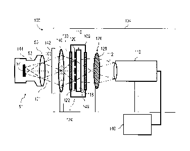
[0021] Fig. 1 shows an example of an infrared scene projector 100, in
accordance with an
embodiment. The infrared scene projector 100 can be used to project a
pixelated image in
the form of an infrared beam 102 along an infrared beam path 101, including
radiation in the
infrared region of the electromagnetic spectrum.
[0022] Broadly described, the infrared scene projector 100 has a housing
104 forming a
support structure receiving both an image projector 110 and an airtight
chamber 106. The
image projector 110 is configured to project a light beam 112 along a light
beam path. The
light beam 112 carries image information and its wavelength lies in the
visible and/or
near-infrared region of the electromagnetic spectrum. As will be described
herebelow, a
computer 146 can be used to forward image data to the image projector 110. The
image can
be projected as a still image or it can be projected in rapid sequence (e.g.,
a video stream).
[0023] As can be understood, the image projector 110 can be a typical
commercially-available image projector. It can have a high-definition (HD)
resolution of
1280 pixels per 720 pixels, a full HD resolution of 1920 pixels per 1080
pixels, a 4K ultra-HD
(UHD) resolution of 3840 pixels per 2160 pixels, a 8K UHD resolution of 7680
pixels per
4320 pixels, a 16K UHD resolution of 15360 pixels per 8640 pixels, or any
other suitable
resolution. In some embodiments, the frame rate of the image projector 110 can
range from
frame-per-second (fps) to 140 fps. However, the image projector 110 can have
any
suitable frame rate adapted to the needs of the intended application. In some
specific
embodiments, the image projector 110 is adapted to project the light beam 112
with a power
CA 02946474 2016-10-25
- 5 -
of 2000-4000 Lumens or, equivalently, 2.5 W to 5 W. In alternate embodiments,
the power
can be greater. As will be understood, any satisfactory image projector 110
can be used. For
instance, in alternate embodiments, the image projector 110 can include a
laser scanning
system which can controllably direct a laser beam onto the array of conversion
units.
[0024] As shown in Fig. 1, the infrared scene projector 100 has a
conversion chip 116
having a substrate 118 secured to the housing 104, and an array of conversion
units 120
received by a face 122 of the substrate 118. In this embodiment, the substrate
118 is planar.
However, the substrate 118 can have any other suitable shape. As depicted, the
array of
conversion units 120 is located inside an airtight chamber 106 and is
optically coupled to the
image projector 110. Indeed, the light beam 112 extends from the image
projector 110 to the
conversion chip 116.
[0025] As can be seen in this example, the conversion units 120 are
optically coupled to
the image projector 110 by using focusing optics 126. As shown, the focusing
optics 126 is
secured to the housing 104 and adapted to receive the light beam 112 emitted
from the
image projector 110 to form an image brought into sharp focus on the array of
conversion
units 120.
[0026] In some embodiments, the focusing optics 126 is provided in the
form of a single
lens 128. However, it is understood that the focusing optics 126 can include
more than one
lens, and that the focusing optics 126 can be included as part of an off-the-
shelf image
projector. In alternate embodiments, the focusing optics 126 includes one or
more reflective
elements. Other suitable embodiments of the focusing optics can be used. For
instance, the
focusing optics 126 may include a type of zoom feature for easy setting of the
size of the
image formed on the array of conversion units 120.
[0027] As will be understood, during use, each of the conversion units
120 of the array
can receive a corresponding portion of the image generated by the image
projector 110.
Each of conversion units 120 can then absorb a fraction of the energy from the
portion of the
light beam 112 incident on it, thereby rising in temperature, and radiate
infrared radiation 130
along the infrared beam path 101 extending from the array of conversion units
120. The
infrared beam path 101 extends outside the housing 104. The infrared radiation
130 can
CA 02946474 2016-10-25
- 6 -
have an emission spectrum approaching that of a blackbody at a given
temperature. The
infrared radiation 130 radiated by each one of the conversion units can then
be collected and
projected in a manner to form, in a specific plane, an infrared image which
can have a
resolution comparable to that of the image projected by the image projector
110.
[0028] In some embodiments, the quantity of conversion units 120 in the
array is chosen
such that any given pixel of the image projector 110 illuminates a plurality
of conversion
units 120 of the array in order to maintain the original resolution of the
image while avoiding
aliasing effects. Accordingly, the quantity of conversion units 120 in the
array can be equal to
a given integer multiple of the quantity of pixels of the image projector 110.
For instance, in
an embodiment wherein the image projector 110 has a HD resolution of 1280
pixels per
720 pixels, the array can have more than 4 million conversion units. Adjacent
conversion
units 120 are separated from one another in order to provide thermal
insulation.
[0029] As depicted in Fig. 1, the infrared scene projector 100 may also
include projecting
optics 140. The projecting optics 140 is secured to the housing 104 and
optically coupled to
the array of conversion units 120. More precisely, the projecting optics 140
is configured to
collect a part of the infrared radiation 130 emitted from the conversion units
120 and to form
an infrared image brought into focus in a given plane in a scene. As can be
seen in this
embodiment, the given plane of the scene generally corresponds to the plane of
the infrared
image sensor 57 of an infrared camera 51 under test and placed in front of the
projecting
optics 140. The image formed in the plane of the infrared image sensor 57 is a
properly-
sized replica of the infrared image formed on the array of conversion units
120. A protective
window 142 can be set in front of the projecting optics 140, and the
protective window 142
can also be part of the projecting optics 140. The projecting optics 140 can
include one or
more than one lens in some other embodiments. In alternate embodiments, the
projecting
optics 140 includes one or more reflective elements. Other suitable
embodiments of the
projecting optics can be used. The projecting optics 140 can have a zoom
feature for ease of
adjusting the size of the image formed on the infrared image sensor 57 of the
infrared
camera. It will be understood that the use of projecting optics is optional.
Indeed, the
objectives of some infrared cameras can be adjusted to provide images of the
conversion
units 120 in focus, without the need for additional optical elements. In
applications where the
CA 02946474 2016-10-25
- 7 -
infrared scene projector 100 is used for testing an infrared camera 51 having
its objective 55
focused to infinity, the projecting optics can be configured to act as an
optical collimator.
[0030] In some embodiments, the airtight chamber 106 is maintained at the
atmospheric
pressure whereas, in some other embodiments, the airtight chamber 106 includes
a vacuum.
The vacuum can be made using a pump (e.g., a dry pump). As can be understood,
a
pressure control mechanism can be used to vary the pressure inside the
airtight
chamber 106. For instance, the pressure inside the airtight chamber 106 can be
variable or
permanent. The airtight chamber 106 can be made of aluminium, stainless steel
or any other
suitable material adapted to maintain and support a given pressure, and thus
the vacuum,
over time. Most commonly available image projectors do not sustain vacuum and
would
thus, along with any other component of this type, be housed outside the
airtight chamber.
[0031] Fig. 2 shows an oblique and partial view of the conversion chip
116, in accordance
with an embodiment. More specifically, there is shown a single one of the
conversion
units 120 as received on a corresponding area 131 of the substrate 118. As
depicted, the
conversion unit 120 has two supporting posts 132 mounted on the substrate 118,
and a
suspended platform 134 held spaced apart by a spacing 136 from the substrate
118 via the
supporting posts 132. In this specific example, the two supporting posts 132
are located at
opposite corners of the conversion unit 120 to provide suitable support. One
or more than
two supporting posts can also be used in alternate embodiments.
[0032] As also shown in Fig. 2, a support arm 137 is provided to connect the
suspended
platform 134 to a corresponding one of the two supporting posts 132. It is
intended that the
length of the support arm 137 can help further thermally insulate the
suspended platform 134
from the substrate 118.
[0033] It is noted that any given conversion unit 120 can absorb optical
energy and then
heat up according to: i) the optical power carried by the portion of the light
beam 112 incident
on the given conversion unit 120, ii) the surface of the conversion unit 120,
iii) the optical
absorption n of the conversion unit 120 in the visible and/or in the near-
infrared, and iv) the
thermal insulation provided by the supporting posts 132 and the support arm
137 relative to
the substrate 118. As shown in this embodiment, each conversion unit 120
consists of a
CA 02946474 2016-10-25
- 8 -
monolithic, continuous structure made up of a given material, and including
the suspended
platform 134, the supporting posts 132 and optional support arms 137.
[0034] As can be understood, once the conversion unit 120 is heated to a given
temperature by the portion of the light beam 112 incident on it and that the
conversion
unit 120 radiates infrared radiation 130 according to the absorbed optical
power, the given
conversion unit 120 can then gradually cool via heat transfer to the substrate
118 via the
support arms 137 and supporting posts 132. The cooling can be characterized by
a time
constant 'I which mainly depends on both the heat capacity C of the conversion
unit 120 and
on the thermal conductance G of the supporting posts 132 and optional arms
137. The time
constant can vary from less than 1 ms to above 30 ms, depending on the shape,
heat
capacity C, and thermal conductance G of a given conversion unit 120. Vacuum
pressure
can also affect the time constant. Based on the factors i), ii), iii) and iv)
recited above, the
temperature of a given conversion unit 120 may rise from a fraction of K to
more than 100 K.
[0035] Varying the pressure inside the airtight chamber 106, e.g., from
lower than
10-3 Torr to about 760 Torr (-1 ATM), can allow, for a given configuration of
the conversion
unit 120, to increase the thermal conductance G of the conversion unit 120
which can
indirectly allow to decrease the time constant T and the maximal temperature
rise.
Therefore, varying the pressure inside the airtight chamber 106 can enable
some control of
the response time and the sensitivity of the conversion unit 120 to the
incoming light
beam 112 without modifying the configuration of the array of conversion units
120.
[0036] Each conversion unit 120 can be made from Silicon Nitride (Si3N4),
Silicon Dioxide
(Si02) or any other material having suitable thermal and mechanical
properties. The
conversion unit 120 can have a square shape having sides ranging from less
than 5 pm to
even more than 35 pm. The size of the conversion unit 120 depends on a desired
spatial
resolution. The suspended platform 134 can have a thickness ranging from 250 A
to 1000 A
or even more. Two adjacent conversion units 120 may be spaced by 0.5 pm to 2
pm. The
supporting posts 132 of a conversion unit 120 can have a square shape, a
rectangular
shape, or any other suitable shape, and can have a width and/or a length
varying from 3 pm
CA 02946474 2016-10-25
- 9 -
to 5 pm. In this embodiment, the height of the supporting posts 132
corresponds to the
spacing 136.
[0037] Each support arm 137 can have, for instance, a thickness ranging
from 250 A to
1000 A, a width ranging from 500 nm to 2000 nm, and a length ranging from 0 to
50 pm. In
the illustrated embodiment, each support arm 137 has a rectilinear shape.
However, in some
other embodiments, the support arm 137 can have an elbow shape, a zig-zag
shape, a
spiral shape, or any other suitable shape. The support arms 137 are sized and
shaped so as
to provide desirable thermal insulation of the suspended platform 134.
Although two support
arms are shown in this embodiment, a single support arm, or more than two
support arms
can be provided in other embodiments.
[0038] In alternate embodiments, such as shown in the conversion chip
116' illustrated in
Fig. 3, the suspended platform 134' of the conversion unit 120' is connected
to the
substrate 118' via two support arms 137' lying in the spacing between the
suspended
platform 134' and the substrate 118'. More specifically, each of the two
support arms 137'
has a first end 139' adapted to receive a corresponding one of the two
supporting posts 132'
and a second end 141' having a second supporting post 143' connecting the
support
arm 137' to the substrate 118'. As it can be seen, each support arm 137'
provides an
intermediate height level between the suspended platform 134' and the
substrate 118'. Each
second supporting post 143' can be similar to the supporting post 132'.
Understandably, the
quantity of support arms 137' is not limited to two. In some embodiments, only
one support
arm 137' is provided whereas more than two support arms 137' are provided in
some other
embodiments.
[0039] The substrate 118 can be made of a material which allows
fabrication of the
conversion units 120 atop thereof. The substrate 118 can have any suitable
dimensions. For
instance, in the case wherein the substrate 118 has a circular shape, the
substrate 118 can
have a diameter ranging from below 25 mm to up to 300 mm, and have a thickness
from
below 0.5 mm to up to 10 mm.
[0040] When the substrate 118 is used in a backlighted (backlit)
configuration, such as the
one shown in Fig. 1, the substrate 118 can be chosen so as to be optically
transparent to
CA 02946474 2016-10-25
- 10 -
visible and/or near-infrared light. For instance, it can be made of glass,
quartz, silicon, or any
other suitable material.
[0041] Fig. 4 shows a sectional view of a row or column of the array of
conversion
units 120, as taken along line 4-4 of Fig. 2, in accordance with an
embodiment. The
spacing 136 between the suspended platform 134 of each of the conversion units
120 and
the substrate 118 can be selected in the range from 1 pm to above 5 pm, and it
remains the
same for all the conversion units 120 of the array. The substrate 118 can also
have an
antireflection coating to prevent undue optical power losses of the light beam
112 when
reflecting upon the other face 122b of the substrate 118.
[0042] In some embodiments, the supporting posts 132 of each conversion
unit 120 are in
direct contact with the face 122 of the substrate 118. Such a direct contact
may simplify the
manufacture of the conversion chip 116. For instance, the supporting posts 132
can be
formed by applying material directly onto the material forming the face 122 of
the
substrate 118, without any additional layer therebetween. Alternately, a
buffer layer could be
deposited on the face 122 of the substrate 118 to provide better adhesion of
the supporting
posts 132 to the substrate 118, or a thin film which is reflective to infrared
radiation but
transparent to visible and near-infrared light could be deposited to improve
the infrared
emission of each conversion unit 120 in the direction of the projecting optics
140 (see Fig.
1).
[0043] As depicted, the infrared scene projector 100 is shown in one
example application.
In this application, as seen on Fig. 1, the infrared scene projector 100 is
used to form
infrared images on the infrared image sensor 57 of an infrared camera 51 for
testing and
characterization purposes. In this specific embodiment, the infrared camera 51
has a camera
housing 53, an infrared image sensor 57 mounted to the camera housing 53, and
an
objective 55 mated to the camera housing 53. As will be understood, the
infrared scene
projector 100 can be used in other applications in which infrared images
representing
desired scenes are required.
[0044] As will be understood, the conversion chip of Fig. 1 is for use
in a transmission
configuration or a backlit configuration. For ease of understanding, reference
is now made to
CA 02946474 2016-10-25
- 11 -
Fig. 5. As depicted in this example, the light beam 112 is projected towards
the left. In this
embodiment, the airtight chamber 106 has a first transmission window 147. The
first
transmission window 147 is, in this embodiment, adapted to be optically
transparent to the
light beam 112 so that most of the optical power carried by the light beam 112
reaches the
substrate 118. For instance, the first transmission window 147 can be made of
BK7, quartz
or any other suitable material. As will be understood, the first transmission
window 147 can
have any suitable shape (e.g., circular) or dimensions which can avoid
obstruction of the
light beam 112. The first transmission window 147 can be installed to the
airtight
chamber 106 using a sealing element such as an 0-ring made of synthetic
rubber, for
instance. The first transmission window 147 can have an antireflection coating
on either or
both faces.
[0045] As mentioned above, in such a backlit configuration, the substrate
118 is made of
a material which is optically transparent to the light beam 112. In this way,
the light
beam 112 is transmitted through the substrate 118 before reaching the
conversion units 120.
In an alternate embodiment, the conversion unit can be used in a front lit
configuration with
the visible and/or near-infrared image projected directly onto the conversion
units, and the
conversion units can radiate infrared radiation across the substrate 118.
Accordingly, the
substrate can be selected to be suitably transparent to infrared radiation.
[0046] As described above, as the conversion units 120 heat upon
absorption of the light
beam 112, the conversion units 120 radiate infrared radiation 130 in all
directions. In this
embodiment, a second transmission window 148 is provided to the airtight
chamber 106.
The second transmission window 148 is optically transparent to the infrared
radiation 130
(including midwave infrared (MWIR) and/or long-wave infrared (LWIR)) such that
the major
part of the infrared radiation 130 can reach the projecting optics 140 (see
Fig. 1). The
second transmission window 148 can be made, for instance, of Germanium (Ge),
Zinc
Selenide (ZnSe) or any other suitable material. It is noted that the second
transmission
window 148 can have any suitable shape (e.g., circular) or dimensions which
can avoid
obstruction of the portion of the infrared radiation 130 which is directed
towards the
projecting optics 140. The second transmission window 148 can be installed to
the airtight
chamber 106 using a sealing element such as an 0-ring made of synthetic
rubber, for
CA 02946474 2016-10-25
- 12 -
instance. The second transmission window 148 can have an antireflection
coating on either
or both faces.
[0047] In some embodiments, such as the one shown in Fig. 5, the
substrate 118 is
secured to the airtight chamber 106 via at least one support. In this specific
embodiment,
two supports 150 are used. In some other embodiments, the substrate 118 can be
secured
directly to the airtight chamber 106.
[0048] In some embodiments, the airtight chamber 106 is adapted, sized
and shaped so
as to form a heat sink which can drain heat away from the substrate 118 via
the two
supports 150.
[0049] In some of these embodiments, each of the two supports 150 includes
a heat
transfer device 151 which can be operated to remove or add heat from or to the
substrate 118 and to transfer the removed or added heat, for instance, towards
or from the
airtight chamber 106 or the housing 104, depending on the embodiments.
Examples of a
heat transfer device include a thermo-electric cooler, a hydraulic cooler
having a cooling fluid
(e.g., water, Freon, liquid nitrogen) flowing through conduits inside or near
the two
supports 150. In these embodiments, the heat transfer device can be used to
vary and
control the temperature of the corresponding support 150 and of the substrate
118 from 77 K
to 325 K. A temperature sensor 149 can be used to monitor and/or control the
temperature
of the substrate 118.
[0050] Fig. 6 shows a sectional and partial view of another example of a
conversion
chip 216, in accordance with another embodiment. Similar elements will bear
similar
reference numerals, but in the 200 series, for ease of reading.
[0051] As shown, the conversion chip 216 has a substrate 218 and an array of
conversion
units 220 received by a face 222 of the substrate 218. In this embodiment,
each one of the
conversion units 220 has one supporting post 232 mounted to the face 222 of
the
substrate 218, and a suspended platform 234 held spaced apart by a spacing 236
from the
face 222 of the substrate 218 via the supporting post 232. As shown in this
embodiment, the
CA 02946474 2016-10-25
- 13 -
supporting post 232 of each of the conversion units 220 is in direct contact
with the
substrate 218.
[0052] In this specific embodiment, an absorber layer 252 covers the
array of conversion
units 220 to increase the amount of energy of the light beam 212 that is
absorbed by the
conversion chip 216 and converted into infrared radiation. In this embodiment,
the absorber
layer 252 is chosen so as to provide adequate absorption of visible and/or
near-infrared light
while being highly emissive in the infrared (including midwave infrared and
long-wave
infrared). The absorber layer 252 can include "Gold Black" or other materials
offering similar
optical absorption properties. The absorber layer 252 has a thickness varying
from 10 A to
50 pm. In alternate embodiments, the absorber layer 252 can be trimmed in-
between
adjacent conversion units 220 to increase the spatial resolution when the
absorber layer 252
is relatively thick. Accordingly, the absorber layer 252 can be trimmed into a
plurality of
distinct absorber layer portions, wherein each of the plurality of absorber
layer portions being
on top of a corresponding one of the conversion units of the array. Such
trimming can be
performed via laser trimming, for instance.
[0053] In alternate embodiments, the suspended platform of each
conversion unit can be
provided with frequency selective surfaces (FSSs) specifically designed so as
to absorb
optical frequencies of the light beam 212 lying in the visible and near-
infrared. An example of
a FSS can include holes of different sizes or other frequency selective
features machined or
patterned directly on the suspended platform 234. Likewise, the holes or
features can be
machined on either a dielectric layer or a metallic layer previously deposited
on the
suspended platform 234.
[0054] As described in the following paragraphs, in some other embodiments,
the
conversion chip 216 is used in a front lighted (front lit) configuration. In
these embodiments,
the light beam 212 is received from above, and not from below such as shown in
Fig. 6.
Accordingly, in these embodiments, the substrate 218 needs not to be optically
transparent
to the visible and/or near-infrared.
CA 02946474 2016-10-25
- 14 -
[0055] Fig. 7 shows another example of an infrared scene projector 300,
in accordance
with an embodiment. Similar elements will bear similar reference numerals, but
in the
300 series, for ease of reading.
[0056] As depicted, the infrared scene projector 300 has a housing 304, an
image
projector 310 secured to the housing 304, and a conversion chip 316 located in
an airtight
chamber 306, the conversion chip having a substrate 318 with a face 322
receiving an array
of conversion units 320. As can be seen, focusing optics 326 is provided to
receive a light
beam 312 emitted from the image projector 310 and to form an image on the
array of
conversion units 320. Projecting optics 340 is provided and optically coupled
to the array of
conversion units 320. The projecting optics 340 collects infrared radiation
330 radiated by
the conversion units 320, and form an image on the image sensor 344 of an
infrared
camera.
[0057] In contrast with the embodiment shown in Fig. 1, the conversion
chip 316 is used
in a front lit configuration instead of being used in a backlit configuration.
Accordingly, the
airtight chamber 306 has a first transmission window 347 which is optically
transparent to
visible and near-infrared light so that the light beam 312 can enter into the
airtight
chamber 306. For instance, the first transmission window 347 can be made of
BK7, quartz or
of any other suitable optical material. As will be understood, the first
transmission
window 347 can have any suitable material shape (e.g., circular) or dimensions
which can
avoid obstruction of the light beam 312. The first transmission window 347 can
be installed
to the airtight chamber 306 using a sealing element such as an 0-ring made of
synthetic
rubber, for instance. The first transmission window 347 can have an
antireflection coating on
either or both faces.
[0058] As shown, the airtight chamber 306 also has a dichroic optical element
359 which
is used to reflect the light beam 312 towards the array of conversion units
320. To do so, the
dichroic optical element 359 is adapted to be optically reflective (e.g.,
using a reflective
coating) to visible and/or near-infrared light.
[0059] In this specific embodiment, the dichroic optical element 359 is
also adapted to be
optically transparent in the infrared (including midwave infrared and/or long-
wave infrared).
CA 02946474 2016-10-25
- 15 -
For instance, the dichroic optical element 359 can be made of Germanium (Ge),
Zinc
Selenide (ZnSe) or of any other suitable material. In this way, the dichroic
optical element
359 can transmit at least a portion of the infrared radiation 330 emitted from
the array of
conversion units 320 to the dichroic optical element 359 so as to reach the
projecting optics
340. As will be understood, the dichroic optical element 359 can have any
suitable material
shape (e.g., circular) or dimensions which can avoid obstruction of the light
beam 312 or the
infrared radiation 330 in either ways. The dichroic optical element 359 can be
installed to the
airtight chamber 306 using a sealing element such as an 0-ring made of
synthetic rubber,
for instance.
[0060] As shown in this embodiment, the first transmission window 347 is set
perpendicular to the array of conversion units 320, and the dichroic optical
element 359
forms an angle of 45 with both the first transmission window 347 and the
array of
conversion units 320. In alternate embodiments, a different angle can be used.
[0061] As will be understood, the dichroic optical element 359 needs not
to be part of the
airtight chamber 306. Fig. 8 shows another example of an infrared scene
projector 400 in
accordance with an embodiment. Similar elements will bear similar reference
numerals, but
in the 400 series, for ease of reading.
[0062] As depicted, the infrared scene projector 400 has a housing 404
having an airtight
chamber 406, an image projector 410 secured to the housing 404, a conversion
chip 416
having a substrate 418 secured to the housing 404 and an array of conversion
units 420
received by a face 422 of the substrate 418. As can be seen, focusing optics
426 is provided
to focus a light beam 412 projected by the image projector 410 onto the array
of conversion
units 420. Projecting optics 440 is provided and optically coupled to the
array of conversion
units 420. The projecting optics 440 collects infrared radiation 430 radiated
by the
conversion units 420, and form an image onto the image sensor of an infrared
camera under
test.
[0063] Similarly to the embodiment shown in Fig. 7, the conversion chip
416 is used in a
front lit configuration. As depicted in this embodiment, the airtight chamber
406 has a first
transmission window 447 which is optically transparent to visible and near-
infrared light and
CA 02946474 2016-10-25
- 16 -
to infrared radiation so as to let the light beam 412 be received on the array
of conversion
units 420 after its reflection onto the dichroic optical element 459. In this
embodiment, the
dichroic optical element 459 is used to reflect the light beam 412, received
from the focusing
optics 426, towards the first transmission window 447. Similarly to the
dichroic optical
element 359 of Fig. 7, the dichroic optical element 459 is adapted to be
optically reflective to
visible and/or near-infrared light and optically transparent to infrared
radiation so as to
transmit at least a portion of the infrared radiation 430 emitted from the
conversion units 420.
As illustrated in this embodiment, the first transmission window 447 is
parallel to the array of
conversion units 420, and the dichroic optical element 459 forms an angle of
45 with both
the first transmission window 447 and the array of conversion units 420. In
alternate
embodiments, a different angle can be used.
[0064] As will be understood, in the embodiments described with reference
to Figs. 7
and 8, the substrate 318 or 418 needs not be optically transparent to visible
and
near-infrared light.
[0065] Fig. 9 shows a schematic representation of the computer 146 shown in
Fig. 1, as a
combination of software and hardware components. The computer 146 is generally
operated
to provide an image feed or signal such that the image projector can project a
light beam in
accordance with some image data. The image data can be representative of a
still image or
a video stream, depending on the embodiment. As shown, the computer 146 can
have one
or more processing units (collectively referred to as "the processing unit
154") and one or
more computer-readable memories (collectively referred to as "the memory
156").
[0066] In some embodiments, the image data are previously created,
collected and
selected, and then stored in an external memory (e.g., hard drive, solid state
drive, USB key)
accessible by the computer 146. In some other embodiments, the image data are
stored on
the memory 156. In alternate embodiments, the image data are stored on an
external
computer via a network.
[0067] The memory 156 can have program instructions 158 stored thereon and
configured to cause the processing unit 154 to generate one or more outputs
based on one
or more inputs. The inputs may comprise one or more signals representative of
the image
CA 02946474 2016-10-25
- 17 -
data and the like. The outputs may comprise one or more signals representative
of image
signal provided to the image projector 110. The image signal can be
transmitted using
communication protocols such as USB, IEEE-488 (FireWire) RS-170, NTSC, VGA,
DVI,
HDMI or any other suitable communication protocol. Before being provided to
the image
projector 110, the image data can be exported into a desired file format such
as JPG, TIFF,
PNG, GIF, BMP, AVI, MPEG 4 AVC (H264), WMV, MOV and the like. The program
instructions can include an image processing application which can process
image data in
accordance with non-uniformity correction (NUC) parameters.
[0068] The processing unit 154 may comprise, for example, any type of
general-purpose
microprocessor or microcontroller, a digital signal processing (DSP)
processor, a central
processing unit (CPU), an integrated circuit, a field programmable gate array
(FPGA), a
reconfigurable processor, other suitably programmed or programmable logic
circuits, or any
combination thereof.
[0069] The memory 156 may comprise any suitable known or other machine
readable
storage medium. The memory 156 may comprise non-transitory computer readable
storage
medium such as, for example, but not limited to, an electronic, magnetic,
optical,
electromagnetic, infrared, or semiconductor system, apparatus, or device, or
any suitable
combination of the foregoing. The memory 156 may include a suitable
combination of any
type of computer memory that is located either internally or externally to
device such as, for
example, random-access memory (RAM), read-only memory (ROM), compact disc read-
only
memory (CDROM), electro optical memory, magneto-optical memory, erasable
programmable read-only memory (EPROM), and electrically-erasable programmable
read-only memory (EEPROM), Ferroelectric RAM (FRAM) or the like. The memory
156 may
comprise any storage means (e.g., devices) suitable for retrievably storing
machine-readable
instructions executable by the processing unit 154.
[0070] Each computer program described herein may be implemented in a
high level
procedural or object oriented programming or scripting language, or a
combination thereof,
to communicate with a computer. Alternatively, the programs may be implemented
in
assembly or machine language. The language may be a compiled or an interpreted
language. Computer-executable instructions may be in many forms, including
program
CA 02946474 2016-10-25
- 18 -
modules, executed by one or more computers or other devices. Generally,
program modules
include routines, programs, objects, components, data structures, etc., that
perform
particular tasks or implement particular abstract data types. Typically the
functionality of the
program modules may be combined or distributed as desired in various
embodiments.
[0071] A method of manufacturing a conversion chip is provided. The method
includes
providing a substrate, depositing a sacrificial layer onto a face of the
substrate, the sacrificial
layer having a thickness based on a desired spacing between the substrate and
the
suspended platform of the conversion units, etching the supporting post
shape(s) in the
sacrificial layer until the substrate is reached, applying material (e.g.,
dielectric) having
desired thermal, mechanical and optical properties directly onto the substrate
inside the
supporting post shape(s) and onto the sacrificial layer to form the optional
support arms and
the suspended platform, depositing the absorber layer or material to form FSS
if desired,
etching contours of the support arms and of the suspended platform, and
removing the
sacrificial layer.
[0072] Another method of manufacturing a conversion chip is provided. The
method
includes providing a substrate, depositing a sacrificial layer onto a face of
the substrate, the
sacrificial layer having a thickness based on a desired spacing between the
substrate and
the suspended platform of the conversion units, etching the supporting post
shape(s) in the
sacrificial layer until the substrate is reached, applying material (e.g.,
dielectric) having
desired thermal, mechanical and optical properties directly onto the substrate
inside the
supporting post shape(s) and onto the sacrificial layer to form the optional
support arms and
the suspended platform, depositing material to form FSS if desired, etching
contours of the
support arms and of the suspended platform, removing the sacrificial layer,
depositing the
absorber layer, and trimming the absorber layer if necessary.
[0073] As can be understood, the examples described above and illustrated
are intended
to be exemplary only. The housing is optional. For instance, in the
embodiments illustrated in
the figures, a housing is used as a support structure to hold the image
projector and the
conversion chip (via the airtight chamber) in a fixed position relative to one
another, defining
a visible beam path leading from the image projector to the conversion chip,
and an infrared
beam path leading away from the conversion chip, outside the airtight chamber
and outside
CA 02946474 2016-10-25
- 19 -
the housing. In alternate embodiments, the airtight chamber itself can include
a structural
enclosure and one or more beam path windows optically communicating
thereacross. The
optical components of the image projector can be secured to one another via a
frame, and
the frame can be secured to the structural enclosure. In still alternate
embodiments, a
dedicated frame can be used as a support structure. The dedicated frame can
directly
receive, secured thereto, the components of the image projector and the
airtight chamber. In
still other embodiments, a supporting structure can be provided in the form of
an optical
table, an optical bench, threaded barrels, mounts, retaining rings, and any
other suitable
structure which can support components of the infrared scene projector and
maintain them
in a fixed position relative to one another. The support structure can be made
of a plurality of
structural elements made integral to one another by any suitable means, such
as threads,
welding, glue, etc. Alternately, the support structure may be monolithic. The
scope is
indicated by the appended claims.