Note: Descriptions are shown in the official language in which they were submitted.
CA 02948408 2016-11-08
WO 2015/168798 PCT/CA2015/050408
METHOD FOR GENERATING RANDOM NUMBERS
AND ASSOCIATED RANDOM NUMBER GENERATOR
FIELD
[0001] The improvements generally relate to the field of random number
generation.
BACKGROUND
[0002] Random numbers have found valuable applications in many fields such as
cryptography, games of chance, scientific calculus and/or statistical studies.
In these
applications, the randomness of the generated random numbers is of great
importance since
their predictability can lead to unsecure communication, to cheating and/or
unreliable
scientific results, for instance.
[0003] Characteristics which are sought from random number generators include
the
ability to produce random numbers at a relatively high rate while using
devices which are
relatively accessible in terms of pricing, bulkiness, etc.
[0004] To satisfy these needs, the methods formerly used typically relied on
pseudo-
random algorithms and/or pseudo-random physical properties of materials. While
random
numbers generated by such methods may seem completely random at first glance
(they may
even pass the statistical test suite for random number generators of the
National Institute of
Standards and Technology (NIST)), such pseudo-random generators are often
based on
deterministic approaches and can thus have a flaw which can allow predicting
the results if
the flaw is ultimately discovered.
[0005] There thus remained room for improvement in providing a suitable device
for
producing random number generation.
SUMMARY
[0006] Contrary to classical mechanics, quantum mechanics presents features
which are
inherently random. There is provided herein a method by which the inherently
random nature
of quantum mechanics can be harnessed for random number generation.
CA 02948408 2016-11-08
WO 2015/168798 PCT/CA2015/050408
- 2 -
[0007] More specifically, there is provided a method for generating
random numbers that
involve charges (negatively-charged electrons or positively-charged holes)
randomly
tunnelling across a quantum tunnelling barrier. The tunnelled charges can thus
generate a
low-level random electrical noise which can be filtered, amplified and sampled
for obtaining
random numbers from a quantum source. The method can be embodied by relatively
simple
electronic components and thus be made readily available on a common board.
[0008] The charges are repelled by the barrier by the mechanism of
classical reflection.
However, because of the quantum tunnelling effect, some charges proceed across
the
barrier and thus succeed in passing from one of the conductors to the other.
This quantum
tunnelling effect is intrinsically random and is thus used to produce random
numbers. By
precisely gauging this quantum tunnelling effect via the difference of
potential (e.g. biasing),
barrier, amplification, filtration, etc, the random number signal stemming
from quantum
tunneling effect can be satisfactorily harnessed and associated to true random
numbers.
Moreover, the gauging and the choice of electronic components can also allow
to produce
such random numbers at a satisfactory rate, using surprisingly simple
electronic
components. The quantum tunnelling barrier can be in the form of an electrical
insulator
sandwiched between conductors, for instance.
[0009] Henceforth, the charges that are able to cross the quantum
tunnelling barrier and
generate the random electrical noise (referred to herein as the random signal)
can do so in a
truly random manner, with quantum tunnelling being known to be a truly random
quantum
process exempt from complex yet deterministic elements.
[0010] Moreover, there is provided a random number generator which comprises a
board
or a Printed Circuit Board (PCB) having a quantum tunnelling barrier mounted
thereon. and
adapted to be connected to a voltage source (source of charges) which can be
either
incorporated directly on the board or provided separately. Since quantum
tunnelling can
involve a large quantity of tunnelled charges which can tunnel across the
quantum tunnelling
barrier at a high rate, such a random number generator can, in theory, allow
very rapid
generation and acquisition of random numbers.
CA 02948408 2016-11-08
WO 2015/168798 PCT/CA2015/050408
- 3 -
[0011] In accordance with one aspect, there is provided a method for
generating at least
one random number, the method comprising the steps of: quantum tunnelling
charges from
one conductor to another conductor across a quantum tunnelling barrier;
receiving a random
signal stemming from the quantum tunnelling of the charges; associating the
random signal
to a random number; and generating a signal indicative of the random number.
[0012] In accordance with another aspect, there is provided a random number
generator
comprising : a board; a quantum tunnelling barrier mounted to the board
between two
conductors and allowing charges to randomly tunnel from one of the conductors
to the other
to generate a random signal; an amplifier mounted to the board, the amplifier
being
connected to one of the two conductors for amplifying the random signal; a
sampling device
mounted to the board and connected to the amplifier for associating, in real
time, the random
signal to at least one random number.
[0013] In accordance with one aspect, there is provided a method for
generating at least
one random number, the method comprising the steps of: applying a difference
of potential
across two conductive layers separated by at least one insulator layer
therebetween, the
difference of potential causing a random quantum tunnelling of charges across
the at least
one insulator, thereby generating a random signal; and associating the random
signal to a
random number.
[0014] In accordance with another aspect, there is provided a random number
generator
comprising: a board; a quantum tunnelling barrier mounted to the board and
having at least
two conductive layers and at least one insulator layer therebetween, the at
least one
insulator layer having two exterior opposite faces each in contact with a
corresponding one
of the two conductive layers, the two conductive layers being connectable to a
first terminal
and a second terminal of a voltage source, the quantum tunneling barrier
allowing charges to
randomly tunnel thereacross to generate a random signal when the voltage
source is
operated; an amplifier mounted to the board, the amplifier connected to either
one two
conductive layers for amplifying the random signal; a sampling device mounted
to the board
and connected to the amplifier for associating in real time the random signal
to at least one
random number.
- 4 -
[0015] Many further features and combinations thereof concerning the present
improvements will appear to those skilled in the art following a reading of
the instant
disclosure.
DESCRIPTION OF THE FIGURES
[0016] In the figures,
[0017] Fig. 1 is a flow chart associated with for generating random
numbers;
[0018] Fig. 2 is a schematic view illustrating an example of a classical
reflection of an
electron against an insulator layer and an example of a quantum tunnelling of
an electron
through an insulator layer;
[0019] Fig. 3 shows an example of a random number mapping in accordance with
an
embodiment of the present invention;
[0020] Fig. 4 is an electrical circuit associated with an example of a
random number
generator;
[0021] Figs. 5A to 5C show schematic views of a quantum tunnelling barrier
having at
least one insulator layer;
[0022] Fig. 6 shows a schematic view an example of a quantum tunnelling
barrier;
[0023] Figs. 7A to 7H show schematic views of the steps of an example of a
photolithography process for fabricating a quantum tunnelling barrier.
DETAILED DESCRIPTION
[0024] Fig. 1 is a flow chart associated with a method for generating random
numbers
based on the principle of random quantum tunnelling of charges (electrons or
holes)
across a quantum tunnelling barrier. As will be discussed in more detail below
with
reference to Fig. 2, the quantum tunnelling barrier can be in the form of a
spacing between
two conductors, across which the charges can either be reflected by classical
reflection or
pass by quantum tunnelling. The random signal stemming from the random
tunnelling of
charges
Date recue / Date received 2021-11-04
CA 02948408 2016-11-08
WO 2015/168798 PCT/CA2015/050408
- 5 -
across the quantum tunnelling barrier is received (sensed, monitored), and the
random
signal can be associated to a random number by a computer, or by electronic
components
based on a real-time amplitude of the signal, to name examples. The process
can be
repeated a satisfactory number of times, at a satisfactory rate.
[0025] The random quantum tunnelling can optionally be assisted by a
difference of
potential applied across the quantum tunnelling barrier. The quantum
tunnelling barrier can
be selected in a manner to cause classical reflection of charges, while
allowing charges to
randomly tunnel thereacross due to quantum processes. The quantum tunnelling
barrier can
be provided in the form of one or more superposed insulating layers as will be
detailed below
with reference to Fig. 5A, 5B, 5C, in which case the conductors can include
conductive
layers applied to the one or more insulating layers, for instance. As the step
of applying the
difference of potential is performed, the difference of potential can prevent
charges from
being conducted from one conductive layer to the other due to an inherent
potential barrier
formed by the at least one insulator layer. Moreover, the insulator layer of
the quantum
tunnelling barrier can harnessed for random tunnelling of charges across the
quantum
tunnelling barrier. The method further comprises a step of generating a random
signal based
on the randomly tunnelled charges.
[0026] Indeed, as the charges are tunnelled from one conductive layer to
the other, a
current or flow of tunnelled charges passes through the insulator layer of the
quantum
tunnelling barrier. These randomly tunnelled charges thus generate the random
signal which
can be processed in a step of associating the random signal received at a
given time to
random digital number.
[0027] As illustrated in Fig. 2, the quantum tunnelling barrier has the
at least one insulator
layer which acts as a reflector for incoming charges. Thus, the charges that
passes through
the at least one insulator layer have done so by randomly crossing the
potential barrier by
quantum tunnelling.
[0028] Moreover, the method may include a step of biasing the difference
of potential for
fixing the difference of potential applied on the two conductive layers.
Moreover, components
of the random signal having frequencies below 0.1 MHz and above 6000 MHz can
be filtered
CA 02948408 2016-11-08
WO 2015/168798 PCT/CA2015/050408
- 6 -
out of the random signal, thus cleaning the random signal from any noise that
can be due to
other electric components connected to the conductive layers. Indeed, the
random signal
can be cleaned from a direct current (DC) portion and from higher frequencies.
[0029] Since the random signal generated by the tunnelled charges
generally is barely
measurable, the method for generating random numbers can include a step of
amplifying the
random signal. The use of the random signal can be limited to components of
the random
signal which have frequencies between 0.1 MHz and 1000 MHz, as suitable to
address
potentially undesired components of noise. In other words, the components of
the random
signal which have a direct current (DC) portion and higher frequencies are not
amplified, for
instance.
[0030] It may be appreciated that the step of associating the random
signal to a random
digital number may include a step referred to herein as sampling the random
signal. Indeed,
the sampling step can associate an instantaneous level (in real time) of the
random signal to
a particular digital number. Once the particular digital number is associated
to the
.. instantaneous level of the random signal, one can discriminate the more
significant bit and
keep only the less significant bits, this has the effect of generating a
uniform distribution of
the random digital number obtained therefrom. For instance, if the step of
sampling
digitalizes the random signal to an 8-bit digital number, one can discriminate
the four more
significant bit and use the four less significant bit.
[0031] Moreover, it is noted that since quantum tunnelling can involve a
large quantity of
tunnelled charges which can tunnel across the quantum tunnelling barrier at a
high rate, the
step of generating a random signal can allow very rapid variation of the
random signal which,
in turn, allow a fast acquisition rate of the random digital numbers. For
instance, sampling
the random signal at a sampling rate above 400 000 kbits/s, preferably above 1
000 Mbits/s
and more preferably above 8 Gbits/s is enabled. It is noted, however, that
more than one
random number generator can be connected in parallel to increase the total
number of
random numbers generated. For instance, by connecting in parallel two random
number
generators each having a generation rate of 8 Gbits/s (1 GB/s), a total
generation rate of 16
Gbits/s (2 GB/s) can be achieved, and so on.
CA 02948408 2016-11-08
WO 2015/168798 PCT/CA2015/050408
- 7 -
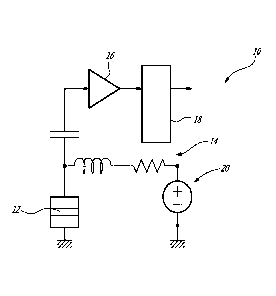
[0032] Fig. 4 shows an electrical circuit 10 associated with an example
of a random
number generator. The random number generator generally comprises a board (not
shown)
on which the electrical circuit 10 is mounted. The electrical circuit 10 of
the random number
generator can include the quantum tunnelling barrier 12, a biasing device 20,
an amplifier
16, a sampling device 18 and a filter 14 which are mountable on the board. For
instance, the
board may be a printed circuit board (PCB) that mechanically supports the
components and
electrically connects the components to one another via conductive tracks
etched from
copper sheets laminated onto a non-conductive substrate.
[0033] As mentioned above, the quantum tunnelling barrier can be provided in
the form of
a quantum tunnelling component having a quantum tunnelling barrier in the form
of one or
more insulator layers sandwiched between conductive layers acting as
conductors. It is
noted that the conductive layers can be made of a metallic material or of a
semiconductor
material, for instance, while the insulator layer can be made of any material
which
satisfactorily inhibits the free conduction of electrons (or holes)
thereacross via classical
reflection. Indeed, any material which can provide an energy barrier which is
crossable by
quantum tunnelling can be used in the quantum tunnelling barrier. For
instance, the insulator
layer can be made of a non-doped semiconductor. Accordingly, the two
conductive layers
can be made of semi-conductor material while the insulator layer can be made
of an
insulator semiconductor. In this example, the insulator semiconductor can have
a band gap
which forces the charges (electrons or holes) to pass thereacross by quantum
tunnelling,
and wherein the two conductive layers can be n-doped or p-doped. The insulator
layer has
two exterior opposite faces each in contact with a corresponding one of the
two conductive
layers and the two conductive layers can be connectable to a first terminal
and a second
terminal of a voltage source. It may be appreciated that the voltage source
may be either
mounted on the board and fixedly connected to the conductive layers of the
quantum
tunnelling barrier or be provided separately thereto.
[0034] In this embodiment, the biasing device 20 can be used to perform a
step of
biasing, the amplifier 16 can be adapted to perform a step of amplifying the
random signal,
the sampling device 18 can be adapted to perform a step of sampling the random
signal and
the filter 14 can be adapted to perform the step of filtering the random
signal. The filter can
CA 02948408 2016-11-08
WO 2015/168798 PCT/CA2015/050408
- 8 -
be connected to the quantum tunnelling barrier, which is, in turn, connected
to the amplifier
and then to the sampling device. When operatively connected one to the others,
the
electrical circuit can instantaneously sample the random signal in order to
obtain a random
number. Moreover, the biasing device can fix the difference of potential
applied to the
quantum tunnelling barrier. Accordingly, the bias of the biasing device can be
adjusted to
encompass any noise that could be incorporated, in the electrical circuit, by
the amplifier or
the sampling device, for instance.
[0035] Figs. 5A to 5C show three examples of the quantum tunnelling
barrier. In these
examples, it can be seen that one or more than one insulator layers can be
used. More
specifically, Fig. 5A shows an insulator layer having a first thickness d1,
while Fig. 5B shows
a quantum tunnelling barrier having two insulator layers, respectively having
a first thickness
d1 and a second thickness d2. Moreover, and in an exemplary manner, Fig. 5C
shows a
quantum tunnelling barrier having three insulator layers, respectively having
a first thickness
d1, a second thickness d2 and a third thickness d3. Although only three
examples have been
provided, the quantum tunnelling barrier may have more than three insulator
layers as well.
The material of the insulating layers can vary and different materials can be
used from one
successive layer to another. Typically, the successive layers can have an
additive effect in
terms of the level of the barrier effect, allowing to reach a desired level
with a plurality of
layers if desired.
[0036] Fig. 6 shows a schematic top view of a quantum tunnelling barrier in
accordance
with the present invention. In this example, the conductive layers of the
quantum tunnelling
barrier are etched from a metallic material such as aluminium and are
laminated onto a non-
conductive substrate such as silicon dioxide. The quantum tunnelling barrier
is illustrated
with a red line and has an overlapping region of approximately 10 pm2 having
dimensions of
1 pm per 10 pm, for instance. Still in this example, the layer of insulator is
comprised
between the two conductive layers where it is noted that the charges can
travel from the top
conductive layer through the bottom conductive layer by quantum tunnelling.
The insulator
layer can be made of aluminium oxide (A1203). It can be seen that the
thickness of the
insulator layer is 1 nm, for instance and can have a resistance of
approximately 50 ohms. It
CA 02948408 2016-11-08
WO 2015/168798 PCT/CA2015/050408
- 9 -
is known that the resistance of the quantum tunnelling barrier can depends on
the
overlapping area.
[0037] Although, the fabrication method of the quantum tunnelling barrier can
vary, an
example fabrication method based on a photolithography technique known as a
Dolan
.. Bridge will now be provided for illustrative purposes with reference to
Fig. 7. In this example,
a photolithography system such as a SF-100 Xpress was used concurrently with
resins
referred to as LOR3OB and S1813. Indeed, the method of fabrication may include
a step of
cleaning a substrate from impurities (a), a step of applying a layer of LOR3OB
resin on the
cleaned substrate, applying a layer of S1813 resin onto the layer of LOS30B
resin (b). Then,
a further step of exposing, to UV light, the S1813 resin everywhere except for
a segment
(which can form a Dolan bridge) can be performed (c). Then, a step of
chemically removing
the layer of S1813 resin which was exposed with UV light can be performed as
well as a
step of chemically removing the layer of LOR3OB for leaving the segment of
layer S1813
(referred to as the Dolan bridge) intact (d). Subsequently, a first conductive
layer can be
evaporated onto the substrate using the Dolan bridge as a mask in order for
the first
conductive layer to lay on the substrate and to protrude from one side of the
Dolan bridge,
and therebelow, as far as the latter allows it (e). Then, an insulator layer
of aluminium oxide
can be evaporated onto the first conductive layer (f). A second conductive
layer can be
evaporated onto the insulator layer, using the other side of the Dolan bridge,
and
therebelow, as far as the latter allows it, forming an overlapping region
where the insulator
layer is sandwiched between the two conductor layers. Finally, the Dolan
bridge can be
removed to uncover a completed quantum tunnelling component.
[0038] Moreover, one skilled in the art may appreciate that by providing
a quantum
tunnelling device mounted directly to a board can lead to a device having a
low cost and
whose manufacturing process can be implemented in specialized facilities such
as fabs, for
instance.
[0039] Although one person skilled in the art may be aware of which hardware
components can be used in the random number generator. In one embodiment, for
instance,
the quantum tunnelling barrier may exhibit a resistance of 54 ohms. The
biasing device can
be a bias-tee Mini-Circuits ZFBT-6GW+. The sampling device can be an 8-bits
data
CA 02948408 2016-11-08
WO 2015/168798 PCT/CA2015/050408
- 10 -
acquisition board having a sampling frequency of 3 billion samplings per
second and
manufactured by UltraviewTM. As mentioned above, the sampling frequency can be
limited
for limiting a correlation between consecutive levels of random signal. For
instance, the
sampling frequency can be limited to 1 billion samplings per second. Moreover,
amplifying
the random signal by 52 dB was found to be sufficient for the random number
generator. The
amplifiers can incorporate two amplifiers Mini-Circuits ZFL-1000LN+ along with
attenuators
Mini-Circuits BW-S3W2+ for tuning the level of amplification of the random
signal. With such
an embodiment, the random number generator can generate up to 4 billons bits
numbers per
second (4 Gbits/s), which is way faster than the closest competitor, the
random number
generator GRANG from LETech, achieving 0.4 Gbits/s.
[0040] It is further noted that when the bias is 0 V (i.e. in the absence
of a biasing device),
the noise is thermal and the charges can pass through the quantum tunnelling
barrier via
quantum tunnelling. Such thermal noise can directly be used as the source of
the random
signal though in the embodiment presented above, it was preferred to use the
quantum
tunnelling effected generated by application of a difference of potential
across the barrier. In
the event where the energy eV is greater than kT, wherein e is the electrical
charge, V is the
bias, k is the Boltzmann constant and T is the absolute temperature in Kelvin
degrees, e.g. V
> 25 mV, the noise can become a shot noise which is proportional to V, i.e.
greater is V,
greater the generated random signal is. In this situation, the contribution
from the other
electrical components of the electrical circuit can be negligible. However, it
can be preferred
to bias V. For instance, the quantum tunnelling barrier can collapse if it
surpasses a
collapsing threshold, which can motivate biasing. In the example described and
illustrated,
suitable use of the quantum tunnelling barrier was achieved at V = 0.25 V.
[0041] Furthermore, it is noted that the sampling device can be provided
in the form of a
digital comparator having one input number being the random signal and another
input
number being zero. When the random signal is positive, then the digital
comparator is
adapted to provide a binary 1, if not, it provides a binary 0. In such a
configuration, known
algorithms can be used to prevent a bias of the zero value of the other input
number.
Accordingly, the digital comparator can be used to obtain a series of
successive and random
binary l's and O's which can be used to provide random numbers. As may be
appreciated by
CA 02948408 2016-11-08
WO 2015/168798 PCT/CA2015/050408
- 11 -
a person skilled in the art, the amplifier and the sampling device could be
limited to
frequencies in the order of the kHz for limiting the cost of the random number
generator.
Moreover, the biasing device may be integrated directly in the amplifier. Such
a biasing
device could bias the difference of potential and also amplify the biased
difference of
potential in the same electrical component. It is further noted that biasing
the difference of
potential can be used as long as it does not interfere with the amplifier.
Although the use of a
sampling device or a digital comparator to convert the random noise to random
numbers is
presented herein, other techniques could also be implemented by a person
skilled in the art.
[0042] It is further noted that the random number generator can be mounted on
a
Universal Serial Bus (USB) device which can provide a portable device
achieving speeds up
to 480 Mb/s with USB 2.0 and even higher with USB 3Ø Alternatively, the
random number
generator can be mounted to a Peripheral Component Interconnect (PCI) device
and
achieve up to 1 Gb/s to 17 Gb/s. Furthermore, the random number generator can
be
implemented directly from an Original Equipment Manufacturer (OEM)
motherboard.
[0043] Increasing the difference of potential can increase the signal.
Alternately, heating
the junction can increase the quantum noise, and thus the signal as well.
[0044] As can be understood, the examples described above and illustrated are
intended
to be exemplary only. The scope is indicated by the appended claims.