Note: Descriptions are shown in the official language in which they were submitted.
CA 02950993 2016-12-08
1
Compact bipolarization excitation assembly for a radiating antenna
element and compact array comprising at least four compact excitation
assemblies
FIELD OF THE INVENTION
The present invention relates to a compact bipolarization excitation
assembly for a radiating antenna element and a compact array comprising at
least four compact excitation assemblies. It applies to any multiple-beam
antenna comprising a focal array operating in low frequency bands and more
particularly to the field of space applications such as satellite
telecommunication in band C, or in band L, or in band S, and to the space
antennas with single-beam global coverage in band C, or in band L, or in
band S. It applies also to the radiating elements for array antennas, notably
in band X or in band Ka.
BACKGROUND OF THE INVENTION
The radiating feeds operating in low frequency bands, for example in
band C, generally comprise very bulky metal horns of significant weight. To
reduce the size of the radiating feed, it is known practice, from the document
FR2959611, to replace the metal horn with stacked Fabry-Perot cavities. This
solution makes it possible to reduce the size of the feeds and exhibits radio
frequency performance levels equivalent to those of a metal horn. However,
this solution is limited to an aperture diameter less than 2.5A, where A
represents the central wavelength, in vacuum, of the frequency band of use.
In order to produce compact feeds of greater radiating aperture, the
document FR 3012917 proposes a solution comprising a compact
bipolarization power splitter comprising four asymmetrical orthomode
transducers OMT, coupled in phase to a power source with dual orthogonal
polarization. These four OMTs are networked together via two power
distributers dedicated to each polarization. This power splitter has a very
small thickness when the OMTs and the two power distributers are situated
in one and the same plane. This solution does however present the
drawback of a mediocre isolation, of the order of 15 dB, between the two
CA 02950993 2016-12-08
2
orthogonal modes of each OMT, which results in inadequate performance
levels for the power splitter. This isolation defect between the two
orthogonal
modes of each OMT is essentially due to the asymmetry of each OMT which
comprises only two lateral access ports spaced apart angularly by 90 about
a main waveguide.
SUMMARY OF THE INVENTION
The aim of the invention is to resolve the problems of the existing
solutions and to propose an alternative solution to the existing radiating
elements, having a radiating aperture diameter of average size lying between
2.5A and 5A, comprising a good isolation between the orthogonal modes, low
losses and being compatible with high-power applications.
For that, the invention relates to a compact bipolarization excitation
assembly consisting of an orthomode transducer OMT comprising two
transmission pathways respectively dedicated to two orthogonal
polarizations, a first and a second power splitter respectively connected to
the two transmission pathways of the OMT, and a first and a second
connection waveguide, the OMT consisting of a cross junction comprising a
central waveguide parallel to an axis Z and four lateral ports respectively
coupled to the central waveguide and oriented in two directions X and Y
orthogonal to one another and to the axis Z. The first power splitter consists
of an input waveguide and of two output ports respectively coupled to a first
and a second lateral port of the OMT, oriented in the direction X, via the
first
and the second respective connection waveguide. The first power splitter is
located on a first lateral side of the OMT, the input waveguide having a
lateral
wall orthogonal to the direction X and extending heightwise parallel to the
axis Z. The two output ports, respectively upper and lower, of the first power
splitter are formed one above the other in the height of said lateral wall of
the
input waveguide, the upper output port being placed facing the first lateral
port of the OMT to which it is connected by the first connection waveguide,
and the first and second connection waveguides have different electrical
lengths, the difference in electrical length between the first and second
connection waveguides being equal to a half-wavelength A/2, where A is the
central wavelength of operation.
CA 02950993 2016-12-08
3
Advantageously, the excitation assembly can comprise several levels
stacked parallel to the plane XY, the OMT and the first connection waveguide
being located in a first level, the second connection waveguide consisting of
a linear section located in a second level, under the orthomode transducer,
and of a section bent to 180 connected to the second lateral port of the
OMT.
Advantageously, the second power splitter can be identical to the first
power splitter and located on a second lateral side of the OMT, orthogonally
to the direction Y.
Advantageously, the second power splitter can consist of an input
waveguide and of two output ports formed one above the other in a lateral
wall of the input waveguide and respectively coupled to a third and a fourth
lateral port of the OMT, oriented in the direction Y, via a third and a fourth
respective connection waveguide, and the third and fourth connection
waveguides have different electrical lengths, the difference in electrical
length
between the third and fourth connection waveguides being equal to a half-
wavelength Al2.
Advantageously, the fourth connection waveguide can consist of a
linear section located in a third level, under the orthomode transducer, and
of
a section bent to 180 connected to the fourth lateral port of the OMT.
Advantageously, the OMT can comprise a symmetrical pyramid
situated at the center of the cross junction.
Alternatively, the second power splitter can be a septum splitter
consisting of an input waveguide provided with an inner wall, called septum,
delimiting two output waveguides parallel to the input waveguide and stacked
in a fourth level under the OMT, parallel to the plane XY, the two output
waveguides of the septum power splitter being respectively connected to the
first and to the second lateral ports of the OMT by fifth and sixth respective
connection waveguides located in a third level, under the OMT, the electrical
lengths of the fifth and sixth connection waveguides being equal. In this
case,
CA 02950993 2016-12-08
4
advantageously, the OMT can comprise a dissymmetrical pyramid situated at
the center of the cross junction.
The invention also relates to a compact array comprising at least four
compact excitation assemblies coupled to one another by two common
power splitters, independent of one another, orthogonal to one another, and
respectively dedicated to the two orthogonal polarizations.
BRIEF DESCRIPTION OF THE DRAWINGS
Other particular features and advantages of the invention will become
clearly apparent hereinafter in the description given by way of purely
illustrative and non-limiting example, with reference to the attached
schematic drawings which represent:
figure 1: a perspective diagram of an exemplary compact
excitation assembly according to a first embodiment of the
invention;
figures 2a and 2b: two sectional diagrams, respectively along
two orthogonal planes XZ and YZ, of the compact excitation
assembly of figure 1, according to the invention;
figures 3a and 3b: two sectional diagrams, respectively along
two orthogonal planes XZ and YZ, of an exemplary compact
excitation assembly, according to a second embodiment of
the invention;
figure 4: a perspective diagram of an exemplary compact
array of four compact excitation assemblies according to the
invention;
figure 5: a perspective schematic view of a first exemplary
assembly of two different orthogonal splitters that can be used
to supply four compact excitation assemblies according to the
invention;
figure 6: a perspective schematic view of a second exemplary
assembly of two identical orthogonal splitters that can be used
to supply four compact excitation assemblies according to the
invention.
CA 02950993 2016-12-08
DETAILED DESCRIPTION
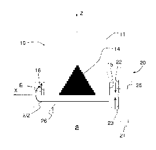
Figure 1 represents a first exemplary compact bipolarization excitation
assembly according to the invention. The excitation assembly, produced in
waveguide technology, comprises several levels stacked one on top of the
5 other, parallel to a plane XY. The excitation assembly comprises an
orthomode transducer OMT 10 and two power splitters 20, 30 respectively
connected to the orthomode transducer, by dedicated connection
waveguides. The orthomode transducer OMT 10, situated in a first level,
consists of a cross junction, known as a "turnstile" junction, comprising a
central waveguide 11 for example of cylindrical geometry, having an axis of
revolution parallel to an axis Z. and four lateral waveguides 12, for example
of rectangular section, diametrically opposite two-by-two, in a plane XY
orthogonal to the axis Z, and coupled at right angles to the central
waveguide. The four lateral waveguides are respectively oriented in two
orthogonal directions X, Y of the plane XY. The central waveguide 11 is
provided with an axial access port 13 and the four lateral waveguides are
respectively provided with four lateral ports oriented in the directions X or
Y.
In transmission, the four lateral ports are input ports and the axial access
port
is an output port. In reception, the input and output ports are reversed and
the operation of the OMT is reversed. The two lateral waveguides oriented in
the direction X and the two lateral waveguides oriented in the direction Y
constitute two pathways of the OMT respectively dedicated to two orthogonal
polarizations P1, P2. The two pathways generate two different propagation
modes in the central waveguide 11 of the OMT. As represented in figures 2a,
2b, 3a, 3b, advantageously, the OMT can further comprise a matching
element, for example in the form of a cone or pyramid 14, placed at the
center of the cross junction and comprising a summit penetrating into the
central waveguide 11, in order to improve the matching of the junction to a
predetermined frequency band of operation and improve the isolation
between the two polarizations. The pyramid 14 or the cone makes it possible
to accompany the electrical field E transmitted by each lateral waveguide of
the OMT to the central waveguide 11 and constitutes an obstacle to the
passage of the electrical field E to the lateral waveguides at right angles.
To
obtain an optimal operation of the orthomode transducer, the two lateral
waveguides of each pathway of the OMT must be supplied by electrical fields
CA 02950993 2016-12-08
6
E of the same amplitude but in phase opposition as figures 2a, 2b, 3a, 3b
show.
The power splitters operate as dividers in transmission and, in
reverse, as combiners in reception. With the operation of each power splitter
in reception being reversed with respect to transmission, the rest of the
description is limited to the operation in transmission. The first power
splitter
20 comprises, in transmission, an input waveguide, of rectangular section,
comprising an input port 21 that can be linked a supply source operating in a
first polarization P1 and two output ports 22, 23, respectively upper and
lower, formed in a lateral wall of the input waveguide. Said lateral wall is
orthogonal to the input port 21 and extends heightwise parallel to the axis Z,
the two output ports being respectively connected to a first and a second
lateral port 15, 16, diametrically opposite, of the orthomode transducer as
figure 2a shows.
The two output ports of the first power splitter 20 are arranged one
below the other, in the height of the lateral wall of the input waveguide
which
constitutes a first output plane parallel to the axis Z and orthogonal to the
direction X. By construction, the electrical fields E on the two output ports
22,
23 of the first power splitter 20 are in phase opposition. To limit the bulk
of
the excitation assembly, the first power splitter 20 is located on a lateral
side
of the orthomode transducer 10, such that the upper output port 22 is placed
in the plane XY, facing a first lateral port 15 of the orthomode transducer to
which it is connected by a first connection waveguide 25. The lower output
port 23 of the first power splitter 20 is linked to a second lateral port 16
of the
orthomode transducer, diametrically opposite the first lateral port, by a
second connection waveguide 26. The second connection waveguide 26
consists of a linear section located in a second level, under the orthomode
transducer, in a plane parallel to the plane XY, and of a bent section,
forming
a 180 turn, connected to the second lateral port 16 of the OMT. For the first
and the second lateral ports of the OMT to be supplied by electrical fields E
in phase opposition, the second connection waveguide 26 has a total
electrical length greater than the electrical length of the first connection
waveguide 25, the difference in electrical length between the first and the
second connection waveguides being equal to a half-wavelength A/2, where A
is the central wavelength of the frequency band of operation of the excitation
CA 02950993 2016-12-08
7
assembly. Thus, the cumulative phase-shift due to the difference in electrical
length and to the turn is equal to 360 and the electrical fields E on the
first
and second lateral ports are in phase opposition.
Regarding the second pathway of the OMT dedicated to the second
polarization P2, the structure of the second power splitter 30 is chosen as a
function of the desired application. Either the two pathways of the OMT
operate in one and the same frequency band, for example transmission Tx,
or they operate in two different frequency bands, for example transmission Tx
and reception Rx.
According to a first embodiment corresponding to an operation of the
two pathways in the same frequency band, as represented in figures 1 and
2b, the second power splitter 30 can be identical to the first power splitter
20,
the two power splitters extending heightwise parallel to the axis Z and being
respectively arranged at right angles to the two directions X and Y. The
second power splitter 30 then comprises an input waveguide and two output
ports formed one above the other in a lateral wall of said input waveguide.
The two output ports 32, 33, upper and lower, are respectively connected to
a third and fourth lateral port 17, 18 of the OMT, dedicated to the second
polarization P2, via a third and a fourth connection waveguide. In this case,
the two output ports 32, 33 of the second power splitter 30 are arranged one
below the other in the heightwise direction of the second power splitter, in a
second output plane parallel to the axis Z and orthogonal to the direction Y.
The upper output port 32 of the second power splitter is placed in the plane
XY, facing a third lateral port 17 of the orthomode transducer to which it is
connected by a third connection guide 27. The lower output port 33 of the
second power splitter is linked to a fourth lateral port 18 of the orthomode
transducer, diametrically opposite the third lateral port, by a fourth
connection
waveguide 28. The fourth connection waveguide 28 is located in a third level
situated under the second connection waveguide 26, on a plane parallel to
the plane XY, and comprises a first linear section and a second section bent
to 180 connected to the fourth lateral port 18 of the OMT. For the electrical
fields E of the third and fourth lateral ports 17, 18 of the OMT to be in
phase
opposition, the fourth connection waveguide 28 has a total electrical length
greater than the electrical length of the third connection waveguide 27, the
CA 02950993 2016-12-08
8
difference in electrical length between the third and the fourth connection
waveguides being equal to a half-wavelength A/2.
In this first embodiment, the two pathways of the OMT operate in
orthogonal polarizations P1, P2 and in the same frequency band. The
geometry of the pyramid 14 of the OMT is symmetrical, its four faces being
identical and having dimensions optimized according to the desired operating
frequency. The lateral and connection waveguides, of rectangular section,
have identical widths.
This very compact excitation assembly, produced in rectangular or
cylindrical metal waveguide technology, makes it possible, in a small bulk, to
excite, in dual polarization, a radiating element coupled to the axial access
port 13 of the OMT and offers the advantages of operating at high radio
frequency RF powers and of having a bandwidth compatible with the
transmission frequency band between 3.7 GHz and 4.2 GHz and
corresponding to band C.
However, because of the constraints on the electrical lengths of the
connection waveguides linking the power splitters to the input ports of the
OMT and the constraints on the widths of the metal waveguides as a function
of the operating frequency, the compact excitation assembly according to this
first embodiment can operate only in frequency bands close to one another
for the two pathways, or in a single frequency band common to the two
pathways of the OMT.
According to a second embodiment represented in figures 3a and 3b,
corresponding to an operation of the two pathways of the OMT in two
different and distinct frequency bands, the second power splitter 30 can have
a structure that is different from the first power splitter 20. For example,
the
two frequency bands can correspond to a transmission band Tx and
respectively to a reception band Rx. In figure 3b, the second power splitter
is
a septum splitter 40 mounted in a fourth level, under the OMT. The septum
splitter 40 comprises an input waveguide provided with an inner wall 41,
called septum, delimiting two output waveguides 42, 43. The septum 41 can
be resistive to improve the isolation between the two output waveguides. The
two output waveguides 42, 43 are parallel to the input waveguide and
stacked parallel to the plane XY. The two output waveguides of the septum
CA 02950993 2016-12-08
9
power splitter are respectively connected to the third and fourth lateral
ports
17, 18 of the OMT by fifth and sixth respective connection waveguides 47, 48
located in a third level, under the OMT, the electrical lengths of the fifth
and
sixth connection waveguides being equal. In this second embodiment, in
order to allow an optimized operation in the two frequency bands of
operation, the transmission frequency band being different from the reception
frequency band, the widths of the lateral and connection waveguides
dedicated to transmission are different from the widths of the waveguides
dedicated to reception. For example, for operation in band C with a
transmission frequency band of between 3.7 and 4.2 GHz and a reception
frequency band of between 5.9 and 6.4 GHz, the wavelength of operation in
reception is less than the wavelength of operation in transmission and the
widths of the waveguides dedicated to the transmission pathway are
therefore greater than the widths of the waveguides dedicated to the
reception pathway. Furthermore, the geometry of the pyramid 14 of the OMT
is dissymmetrical, as figures 3a and 3b show, two of its four faces having
smaller dimensions, optimized for operation in the reception frequency band
and the other two faces having larger dimensions, optimized for operation in
the transmission frequency band. In particular, seen from the lateral
rectangular waveguides of the OMT, the pyramid is wider in transmission
than in reception.
Each compact excitation assembly can be used alone to supply an
individual radiating element coupled at the output of the axial waveguide of
the OMT. Alternatively, as illustrated in figure 4, several compact excitation
assemblies can be coupled to one another in an array, for example in fours
or sixteens, by using two orthogonal power splitters, independent of one
another, and fitted one above the other, the two power splitters being
respectively dedicated to the two orthogonal polarizations P1 and P2 and
common to all the OMTs of the array. Figure 5 illustrates a first exemplary
assembly of two orthogonal power splitters in which the two power splitters
51, 52 are not identical because they are dedicated to two different frequency
bands, for example Rx and Tx. Figure 6 illustrates a second exemplary
assembly of two orthogonal power splitters in which the two power splitters
51, 55 are identical because they are dedicated to two identical frequency
bands, for example Tx. The two different power splitters 51, 52, or the two
CA 02950993 2016-12-08
identical power splitters 51, 55, are respectively connected to the four OMTs
of the array via connection waveguides and ensure the splitting and the
dividing, or the combining, of the power between the different OMTs of the
duly formed compact array. In figure 4, the compact array comprises four
5 distinct OMTs coupled to one another by two orthogonal power splitters,
common to all the OMTs, including dividers/combiners of power by eight. The
different individual power splitters corresponding to one and the same
polarization and dedicated to each OMT of the array are thus grouped
together and incorporated in the common power splitter corresponding to
10 said polarization. Each power splitter is respectively connected to all
the
OMTs of the array by the respective connection waveguides dedicated to
each of the corresponding compact excitation assemblies. The compact
array can be intended to supply a radiating feed 50 with four accesses having
an aperture four times greater than an individual radiating element and
operating in band C or, alternatively, to supply four individual radiating
feeds.
Each power splitter 51, 52, 55 comprises a respective input port 53, 54, 56
that can be linked to a respective supply source. The radiating feed 50,
coupled to the output ports of the central waveguides 11 of the OMTs of the
different excitation assemblies of the array can, for example, be a Fabry-
Perot cavity as in figure 4 in the case of an array of four compact excitation
assemblies. Similarly, a compact excitation assembly of even greater
aperture can be produced by linking 16 excitation assemblies in an array by
two orthogonal power splitters including power dividers by thirty-two.
Although the invention has been described in conjunction with
particular embodiments, it is clear that it is in no way limited thereto and
that
it comprises all the technical equivalents of the means described as well as
the combinations thereof provided the latter fall within the scope of the
invention.