Note: Descriptions are shown in the official language in which they were submitted.
CA 02951228 2016-12-05
WO 2016/007234
PCT/US2015/033351
WIRELESS POWER TRANSFER THROUGH A METAL OBJECT
FIELD
[0001] The
described technology generally relates to wireless power. More
specifically, the disclosure is directed to devices, systems, and methods
related to
transferring wireless power by a wireless power charging system through a
metal object.
BACKGROUND
[0002] In
wireless power applications, wireless power charging systems may
provide the ability to charge and/or power electronic devices without
physical, electrical
connections, thus reducing the number of components required for operation of
the
electronic devices and simplifying the use of the electronic device. Such
wireless power
charging systems may comprise a transmitter antenna and other transmitting
circuitry
configured to generate a magnetic field that may induce a current in a
receiver antenna
that may be connected to the electronic device to be charged or powered
wirelessly.
Some portable electronic devices may have housings made of various materials
including
metal. As it is desirable to incorporate wireless power circuitry into various
portable
electronic devices, there is a need for a system and method for performing
wireless power
transfer through metal objects.
SUMMARY
[0003] The
implementations disclosed herein each have several innovative
aspects, no single one of which is solely responsible for the desirable
attributes of the
invention. Without limiting the scope, as expressed by the claims that follow,
the more
prominent features will be briefly disclosed here. After considering this
discussion, one
will understand how the features of the various implementations provide
several
advantages over current wireless charging systems.
[0004] An
apparatus for wirelessly receiving power via a magnetic field. The
apparatus includes a metal cover including an inner portion and an outer
portion. The
outer portion is configured to form a loop around the inner portion of the
metal cover.
The outer portion is configured to inductively couple power via the magnetic
field. The
apparatus further includes a receive circuit electrically coupled to the outer
portion and
configured to receive a current from the outer portion generated in response
to the
-1-
CA 02951228 2016-12-05
WO 2016/007234
PCT/US2015/033351
magnetic field. The receive circuit is configured to charge or power a load
based on the
current.
[0005] In
another aspect an apparatus for transmitting wireless power is
provided. The apparatus includes a metal cover including an inner portion and
an outer
portion, the outer portion configured to form a loop around the inner portion
of the metal
cover. The metal cover is configured to generate a wireless power field based
on a
current received from a power source.
[0006] In yet
another aspect an apparatus for receiving wireless power is
provided. The apparatus includes a metal ring comprising at least one slot
configured to
make the metal ring discontinuous at least one location. The apparatus further
includes a
receive circuitry coupled to the metal ring and configured to receive a
current from the
metal ring. The metal ring is configured to generate the current based on
exposure to a
magnetic field.
[0007] In yet
another aspect, a method for wirelessly receiving power via a
magnetic field is provided. The method includes wirelessly receiving power via
a metal
cover comprising an inner portion and an outer portion. The outer portion is
configured
to form a loop around the inner portion of the metal cover. The outer portion
is
configured to inductively couple power via the magnetic field. The method
further
includes powering or charging a load based on the receive power.
[0008] In yet
another aspect, an apparatus for receiving wireless power from a
magnetic field is provided. The apparatus includes conducting means for
partially
housing a portable electronic device. The conducting means includes an inner
portion
and an outer portion. The outer portion is configured to form a loop around
the inner
portion of the conducting means. The outer portion includes means for
inductively
coupling power via the magnetic field. The apparatus further includes means
for
powering or charging a load based on power receiving via the outer portion.
[0009] In yet
another aspect, an apparatus for wirelessly receiving power is
provided. The apparatus includes a housing portion configured to form a back
of a
portable electronic device. The housing has a first dimension. The housing
portion
includes a metal portion having a second dimension the same size as or having
a size that
covers a majority of the first dimension of the housing portion. At least a
portion of the
metal portion is configured to inductively couple power via a magnetic field
at a level
sufficient for charging or powering a load of the portable electronic device.
The
-2-
CA 02951228 2016-12-05
WO 2016/007234
PCT/US2015/033351
apparatus further includes an electrical connection electrically coupled to
the metal
portion and configured to provide received power to the portable electronic
device.
BRIEF DESCRIPTION OF THE DRAWINGS
[0010] The
above-mentioned aspects, as well as other features, aspects, and
advantages of the present technology will now be described in connection with
various
implementations, with reference to the accompanying drawings. The illustrated
implementations, however, are merely examples and are not intended to be
limiting.
Throughout the drawings, similar symbols typically identify similar
components, unless
context dictates otherwise. Note that the relative dimensions of the following
figures may
not be drawn to scale.
[0011] FIG. 1
is a functional block diagram of a wireless power transfer
system, in accordance with one exemplary implementation.
[0012] FIG. 2
is a functional block diagram of a wireless power transfer
system, in accordance with another exemplary implementation.
[0013] FIG. 3
is a schematic diagram of a portion of transmit circuitry or
receive circuitry of FIG. 2 including a transmit or receive antenna, in
accordance with
exemplary implementations.
[0014] FIG. 4
is a functional block diagram of a transmitter that may be used
in an inductive power transfer system, in accordance with exemplary
implementations of
the invention.
[0015] FIG. 5
is a functional block diagram of a receiver that may be used in
the inductive power transfer system, in accordance with exemplary
implementations of
the invention.
[0016] FIG. 6A
is a diagram of a metal back cover used in a portable
electronic device.
[0017] FIG. 6B
is a diagram of an isometric view of the metal back cover of
FIG. 6A.
[0018] FIG. 6C
is a diagram of an exploded isometric view of the metal back
cover of FIG. 6A.
[0019] FIG. 7A
is a diagram of an isometric view of a metal back cover
configured for inductive power transfer, in accordance with one exemplary
implementation.
-3-
CA 02951228 2016-12-05
WO 2016/007234
PCT/US2015/033351
[0020] FIG. 7B
is a diagram of an exploded isometric view of the metal back
cover of FIG. 7A.
[0021] FIG. 8A
is a diagram of a perspective view of a metal back cover
further enlarged and having additional components, in accordance with one
exemplary
implementation.
[0022] FIG. 8B
is a diagram of a perspective view of a metal back cover
having additional components, in accordance with one exemplary implementation.
[0023] FIG. 8C
is a diagram of an isometric view of a metal back cover
comprising the additional components described in relation to FIG 8A.
[0024] FIG. 8D
is a diagram of an exploded isometric view of a metal back
cover as described in FIG. 8C.
[0025] FIG. 9A
is a diagram of a metal band configured to operate as a loop
antenna for inductive power transfer, in accordance with another exemplary
implementation.
[0026] FIG. 9B
is a diagram of the metal band of FIG. 9A configured to
operate as a loop antenna for inductive power transfer, in accordance with
another
exemplary implementation.
[0027] FIG. 10
is a flowchart of an exemplary method of receiving wireless
power via a wireless field, in accordance with another exemplary
implementation.
[0028] FIG. 11
is a flowchart of an exemplary method of transmitting wireless
power via a wireless field, in accordance with another exemplary
implementation.
DETAILED DESCRIPTION
[0029] In the
following detailed description, reference is made to the
accompanying drawings, which form a part of the present disclosure. The
illustrative
implementations described in the detailed description, drawings, and claims
are not meant
to be limiting. Other implementations may be utilized, and other changes may
be made,
without departing from the spirit or scope of the subject matter presented
here. It will be
readily understood that the aspects of the present disclosure, as generally
described
herein, and illustrated in the Figures, can be arranged, substituted,
combined, and
designed in a wide variety of different configurations, all of which are
explicitly
contemplated and form part of this disclosure.
[0030] Wireless
power transfer may refer to transferring any form of energy
associated with electric fields, magnetic fields, electromagnetic fields, or
otherwise from
-4-
CA 02951228 2016-12-05
WO 2016/007234
PCT/US2015/033351
a transmitter to a receiver without the use of physical electrical conductors
(e.g., power
may be transferred through free space). The power output into a wireless field
(e.g., a
magnetic field or an electromagnetic field) may be received, captured by, or
coupled by a
"receive antenna" to achieve power transfer.
[0031] The
terminology used herein is for the purpose of describing particular
implementations only and is not intended to be limiting of the disclosure. It
will be
understood by those within the art that if a specific number of a claim
element is
intended, such intent will be explicitly recited in the claim, and in the
absence of such
recitation, no such intent is present. For example, as used herein, the
singular forms "a",
"an" and "the" are intended to include the plural forms as well, unless the
context clearly
indicates otherwise. As used herein, the term "and/or" includes any and all
combinations
of one or more of the associated listed items. It will be further understood
that the terms
"comprises," "comprising," "includes," and "including," when used in this
specification,
specify the presence of stated features, integers, steps, operations,
elements, and/or
components, but do not preclude the presence or addition of one or more other
features,
integers, steps, operations, elements, components, and/or groups thereof
Expressions
such as "at least one of," when preceding a list of elements, modify the
entire list of
elements and do not modify the individual elements of the list.
[0032] FIG. 1
is a functional block diagram of a wireless power transfer
system 100, in accordance with one exemplary implementation. Input power 102
is
provided to a transmitter 104 from a power source (not shown in this figure)
to generate a
wireless (e.g., magnetic or electromagnetic) field 105 for performing energy
transfer. A
receiver 108 couples to the wireless field 105 and generates output power 110
for storing
or consumption by a device (not shown in this figure) coupled to the output
power 110.
Both the transmitter 104 and the receiver 108 are separated by a distance 112.
[0033] The
receiver 108 may wirelessly receive power when the receiver 108
is located in the wireless field 105 generated by the transmitter 104. The
transmitter 104
includes a transmit antenna or coil 114 for transmitting energy to the
receiver 108 via the
wireless field 105. The receiver 108 includes a receive antenna or coil 118
for receiving
or capturing energy transmitted from the transmitter 104 via the wireless
field 105. The
wireless field 105 corresponds to a region where energy output by the
transmitter 104
may be captured by the receiver 108. In some implementations, the wireless
field 105
may correspond to the "near-field" of the transmitter 104. The near-field may
correspond
to a region in which there are strong reactive fields resulting from the
currents and
-5-
CA 02951228 2016-12-05
WO 2016/007234
PCT/US2015/033351
charges in the transmit coil 114 that minimally radiate power away from the
transmit coil
114. The near-field may correspond to a region that is within about one
wavelength (or a
fraction thereof) of the transmit coil 114.
[0034] In one
exemplary implementation, the wireless field 105 may be a
magnetic field and the transmitter 104 and the receiver 108 are configured to
inductively
transfer power. The transmitter 104 and the receiver 108 may further be
configured
according to a mutual resonant relationship. When the resonant frequency of
the receiver
108 and the resonant frequency of the transmitter 104 are substantially the
same or very
close, transmission losses between the transmitter 104 and the receiver 108
are reduced.
Resonant inductive coupling techniques may allow for improved efficiency and
power
transfer over various distances and with a variety of inductive coil
configurations. When
configured according to a mutual resonant relationship, in an implementation,
the
transmitter 104 outputs a time varying magnetic field with a frequency
corresponding to
the resonant frequency of the transmit coil 114. When the receiver 108 is
within the
wireless field 105, the time varying magnetic field may induce a current in
the receive
coil 118. When the receive coil 118 is configured to resonate at the frequency
of the
transmit coil 114, energy may be more efficiently transferred. The alternating
current
(AC) induced in the receive coil 118 may be rectified as described above to
produce
direct current (DC) that may be provided to charge or to power a load (not
shown).
[0035] FIG. 2
is a functional block diagram of a wireless power transfer
system 200, in accordance with an exemplary implementation. The system 200
includes
a transmitter 204 and a receiver 208. The transmitter 204 includes transmit
circuitry 206
that includes an oscillator 222, a driver circuit 224, and a filter and
matching circuit 226.
The oscillator 222 may be configured to generate a signal at a desired
frequency that is
adjusted in response to a frequency control signal 223. The oscillator 222
provides the
oscillator signal to the driver circuit 224. The driver circuit 224 is
configured to drive a
transmit antenna 214 at, for example, a resonant frequency of the transmit
antenna 214
based on an input voltage signal (VD) 225. The driver circuit 224 may be a
switching
amplifier configured to receive a square wave from the oscillator 222 and
output a sine
wave or square wave.
[0036] The
filter and matching circuit 226 filters out harmonics or other
unwanted frequencies and match the impedance of the transmitter 204 to the
transmit
antenna 214. As a result of driving the transmit antenna 214, the transmit
antenna 214
-6-
CA 02951228 2016-12-05
WO 2016/007234
PCT/US2015/033351
may generate a wireless field 205 to wirelessly output power at a level
sufficient for
charging a battery 236, for example.
[0037] The
receiver 208 includes receive circuitry 210 that includes a
matching circuit 232 and a rectifier circuit 234. The matching circuit 232 may
match the
impedance of the receive circuitry 210 to a receive antenna 218. The rectifier
circuit 234
may generate a direct current (DC) power output from an alternate current (AC)
power
input to charge a battery 236. The receiver 208 and the transmitter 204 may
additionally
communicate on a separate communication channel 219 (e.g., Bluetooth, Zigbee,
cellular,
etc). The receiver 208 and the transmitter 204 may alternatively communicate
via in-
band signaling using characteristics of the wireless field 205.
[0038] FIG. 3
is a schematic diagram of a portion of the transmit circuitry 206
or the receive circuitry 210 of FIG. 2, in accordance with exemplary
implementations. As
illustrated in FIG. 3, transmit or receive circuitry 350 includes an antenna
352. The
antenna 352 may also be referred to or be configured as a "loop" antenna 352.
The
antenna 352 may also be referred to herein or be configured as a "magnetic"
antenna or
an induction coil. The term "antenna" generally refers to a component that
wirelessly
outputs or receives energy for coupling to another "antenna." The antenna 352
may also
be referred to as a coil or inductor of a type that is configured to
wirelessly output or
receive power. As used herein, the antenna 352 is an example of a "power
transfer
component" of a type that is configured to wirelessly output and/or receive
power. The
antenna 352 may include an air core or a physical core such as a ferrite core
(not shown in
this figure).
[0039] The
antenna 352 may form a portion of a resonant circuit configured to
resonate at a resonant frequency. The resonant frequency of the loop or
magnetic antenna
352 is based on the inductance and capacitance. Inductance may be simply the
inductance created by the antenna 352, whereas, a capacitor may be added to
create a
resonant structure at a desired resonant frequency. As a non-limiting example,
a
capacitor 354 and a capacitor 356 are added to the transmit or receive
circuitry 350 to
create a resonant circuit that resonates at a desired frequency of operation.
Accordingly,
for larger diameter antennas, the size of capacitance needed to sustain
resonance may
decrease as the diameter or inductance of the loop increases. Other resonant
circuits
formed using other components are also possible.
[0040] As
another non-limiting example, a capacitor (not shown) may be
placed in parallel between the two terminals of the circuitry 350. For
transmit antennas, a
-7-
CA 02951228 2016-12-05
WO 2016/007234
PCT/US2015/033351
signal 358, with a frequency that substantially corresponds to the resonant
frequency of
the antenna 352, may be an input to the antenna 352.
[0041] FIG. 4
is a simplified functional block diagram of a transmitter 400
that may be used in an inductive power transfer system, in accordance with
exemplary
implementations of the invention. The transmitter 400 includes transmit
circuitry 402 and
a transmit antenna 404 operably coupled to the transmit circuitry 402. In some
implementations, the transmit antenna 404 is configured as the transmit
antenna 214 as
described above in reference to FIG. 2. In some implementations, the transmit
antenna
404 is or may be referred to as a coil (e.g., an induction coil). In some
implementations,
the transmit antenna 404 is associated with a larger structure, such as a pad,
table, mat,
lamp, or other stationary configuration. In some implementations, the transmit
antenna
404 is configured to generate an electromagnetic or magnetic field within a
charging
region. In an exemplary implementation, the transmit antenna 404 is configured
to
transmit power to a receiver device within the charging region at a power
level sufficient
to charge or power the receiver device.
[0042] The
transmit circuitry 402 may receive power through a number of
power sources (not shown). The transmit circuitry 402 may include various
components
configured to drive the transmit antenna 404. In some exemplary
implementations, the
transmit circuitry 402 may be configured to adjust the transmission of
wireless power
based on the presence and constitution of the receiver devices as described
herein. As
such, the transmit circuitry 402 may provide wireless power efficiently and
safely.
[0043] The
transmit circuitry 402 includes a controller 415. In some
implementations, the controller 415 may be a micro-controller or a processor.
In other
implementations, the controller 415 may be implemented as an application-
specific
integrated circuit (ASIC). The controller 415 may be operably connected,
directly or
indirectly, to each component of the transmit circuitry 402. The controller
415 may be
further configured to receive information from each of the components of the
transmit
circuitry 402 and perform calculations based on the received information. The
controller
415 may be configured to generate control signals for each of the components
that may
adjust the operation of that component. As such, the controller 415 may be
configured to
adjust the power transfer based on a result of the calculations performed by
it.
[0044] The
transmit circuitry 402 further includes a memory 420 operably
connected to the controller 415. The memory 420 may comprise random-access
memory
(RAM), electrically erasable programmable read only memory (EEPROM), flash
-8-
CA 02951228 2016-12-05
WO 2016/007234
PCT/US2015/033351
memory, or non-volatile RAM. The memory 420 may be configured to temporarily
or
permanently store data for use in read and write operations performed by the
controller
415. For example, the memory 420 may be configured to store data generated as
a result
of the calculations of the controller 415. As such, the memory 420 allows the
controller
415 to adjust the transmit circuitry 402 based on changes in the data over
time.
[0045] The
transmit circuitry 402 further includes an oscillator 412 operably
connected to the controller 415. In some implementations, the oscillator 412
is
configured as the oscillator 222 as described above in reference to FIG. 2.
The oscillator
412 may be configured to generate an oscillating signal at the operating
frequency of the
wireless power transfer. In some implementations, the transmit circuitry 402
is
configured to operate at the 6.78 MHz ISM frequency band. The controller 415
may be
configured to selectively enable the oscillator 412 during a transmit phase
(or duty cycle).
The controller 415 may be further configured to adjust the frequency or a
phase of the
oscillator 412 which may reduce out-of-band emissions, especially when
transitioning
from one frequency to another. As described above, the transmit circuitry 402
may be
configured to provide an amount of charging power to the transmit antenna 404
via the
signal, which may generate energy (e.g., magnetic flux) about the transmit
antenna 404.
[0046] The
transmit circuitry 402 further includes a driver circuit 414
operably connected to the controller 415 and the oscillator 412. The driver
circuit 414
may be configured as the driver circuit 224 as described above in reference to
FIG. 2.
The driver circuit 414 may be configured to drive the signals received from
the oscillator
412, as described above.
[0047] The
transmit circuitry 402 further includes a low pass filter (LPF) 416
operably connected to the transmit antenna 404. The low pass filter 416 may be
configured as the filter portion of the matching circuit 418 as described
above in reference
to FIG. 2. In some exemplary implementations, the low pass filter 416 may be
configured
to receive and filter an analog signal of current and an analog signal of
voltage generated
by the driver circuit 414. In some implementations, the low pass filter 416
may alter a
phase of the analog signals. The low pass filter 416 may cause the same amount
of phase
change for both the current and the voltage, canceling out the changes. In
some
implementations, the controller 415 may be configured to compensate for the
phase
change caused by the low pass filter 416. The low pass filter 416 may be
configured to
reduce harmonic emissions to levels that may prevent self-jamming. Other
exemplary
-9-
CA 02951228 2016-12-05
WO 2016/007234
PCT/US2015/033351
implementations may include different filter topologies, such as notch filters
that
attenuate specific frequencies while passing others.
[0048] The
transmit circuitry 402 may further include a fixed impedance
matching circuit 418 operably connected to the low pass filter 416 and the
transmit
antenna 404. The matching circuit 418 may be configured as the matching
portion of the
filter and matching circuit 226 as described above in reference to FIG. 2. The
matching
circuit 418 may be configured to match the impedance of the transmit circuitry
402 to the
transmit antenna 404. Other exemplary implementations may include an adaptive
impedance match that may be varied based on measurable transmit metrics, such
as the
measured output power to the transmit antenna 404 or a DC current of the
driver circuit
414.
[0049] The
transmit circuitry 402 may further comprise discrete devices,
discrete circuits, and/or an integrated assembly of components.
[0050] Transmit
antenna 404 may be implemented as an antenna strip with the
thickness, width and metal type selected to keep resistive losses low. In
an
implementation, the transmit antenna 404 may generally be configured for
association
with a larger structure such as a pad, table, mat, lamp or other less portable
configuration.
In an exemplary application where the transmit antenna 404 may be larger in
diameter
relative to the receive antenna, the transmit antenna 404 will not necessarily
need a large
number of turns to obtain a reasonable inductance to form a portion of a
resonant circuit
tuned to a desired operating frequency.
[0051] FIG. 5
is a block diagram of a receiver 500, in accordance with an
implementation of the present invention. A receiver 500 includes a receive
circuitry 502,
a receive antenna 504, and a load 550. The receiver circuitry 502 is
electrically coupled
to the load 550 for providing received charging power thereto. It should be
noted that
receiver 500 is illustrated as being external to load 550 but may be
integrated into load
550. The receive antenna 504 is operably connected to the receive circuitry
502. The
receive antenna 504 may be configured as the receive antenna 218 as described
above in
reference to FIG. 2/FIG. 3. In some implementations, the receive antenna 504
may be
tuned to resonate at a frequency similar to a resonant frequency of the
transmit antenna
404, or within a specified range of frequencies, as described above. The
receive antenna
504 may be similarly dimensioned with transmit antenna 404 or may be
differently sized
based upon the dimensions of the load 550. The receive antenna 504 may be
configured
to couple to a magnetic field generated by the transmit antenna 404 (FIG. 4),
as described
-10-
CA 02951228 2016-12-05
WO 2016/007234
PCT/US2015/033351
above, and provide an amount of received energy to the receive circuitry 502
to power or
charge the load 550.
[0052] The
receive circuitry 502 is operably coupled to the receive antenna
504 and the load 550. The receive circuitry may be configured as the receive
circuitry
210 as described above in reference to FIG. 2. The impedance presented to the
receive
antenna by the receive circuitry 502 may be configured to match an impedance
of the
receive antenna 504 (e.g., via the matching circuit 512) which may increase
efficiency.
The receive circuitry 502 may be configured to generate power based on the
energy
received from the receive antenna 504. The receive circuitry 502 may be
configured to
provide the generated power to the load 550. In some implementations, the
receiver 500
may be configured to transmit a signal to the transmitter 400 indicating an
amount of
power received from the transmitter 400.
[0053] The
receive circuitry 502 includes a processor-signaling controller 516
configured to coordinate the processes of the receiver 500.
[0054] The
receive circuitry 502 includes power conversion circuitry 506 for
converting a received energy source into charging power for use by the load
550. The
power conversion circuitry 506 includes an AC-to-DC converter 508 coupled to a
DC-to-
DC converter 510. The AC-to-DC converter 508 rectifies the AC from the receive
antenna 504 into DC while the DC-to-DC converter 510 converts the rectified
energy
signal into an energy potential (e.g., voltage) that is compatible with the
load 550.
Various AC-to-DC converters are contemplated including partial and full
rectifiers,
regulators, bridges, doublers, as well as linear and switching converters.
[0055] The
receive circuitry 502 may further include switching circuitry 512
configured to connect the receive antenna 504 to the power conversion
circuitry 506 or
alternatively for disconnecting the power conversion circuitry 506 from the
receive
antenna 504. Disconnecting the receive antenna 504 from the power conversion
circuitry
506 not only suspends charging of the load 550, but also changes the "load" as
"seen" by
the transmitter 400 (FIG. 4) as is explained more fully below.
[0056] The
wireless power circuitry described above, and particularly the
receive circuitry 502, is intended to be incorporated into a variety of
portable electronic
devices. Some portable devices may have housings or other portions that are
made of a
variety of materials including metal. As metal housing portions may be
affected by
wireless power transfer, certain aspects of various implementations described
herein are
related to incorporating wireless power circuitry into devices with metal
covers/housings.
-11-
CA 02951228 2016-12-05
WO 2016/007234
PCT/US2015/033351
[0057] FIG. 6A
is a diagram of a metal back cover 602 used in a portable
electronic device (not shown). The metal back cover 602 shown may be a back
cover that
physically couples to the back of a portable electronic device (e.g., a cell-
phone, or a
tablet, or the like) or forms a back portion of a housing of a portable
electronic device.
For example, the metal back cover 602 may mechanically couple to the back of a
portable
electronic device. The metal back cover 602 may be mostly metal (e.g.,
aluminum) but
may have other non-metal components as well for various purposes (e.g.,
holding various
portions of the cover together). As shown in FIG. 6A, a portion represents the
metal back
cover 602 of a device (e.g., a cell phone or a media device, etc.). A
plurality of horizontal
slots 604 and 606 running across the metal back cover 602 in the horizontal
direction are
provided (the term "slot" as described herein may refer to any gap of any
dimension or
other non-conductive area or material). The top horizontal slot 604 is a slot
across the top
of the metal back cover 602, and the bottom horizontal slot 606 is a slot
across the bottom
of the metal back cover 602. The horizontal slots 604 and 606, represented by
a white
space between shaded portions of the metal back cover 602, are not connected
to each
other. A vertical slot 608 connects a hole 610 (e.g., a camera hole) or other
non-metal
portion in the metal back cover 602 to the top horizontal slot 604. A
rectangular near
field communication ("NFC") coil 612 surrounds the hole 610 in the metal back
cover
602 while staying entirely below the top horizontal slot 604. In other
implementations,
the NFC coil 612 may be of any other shape. A source 614 (e.g., a current
feed, a power
source, etc.) is shown coupled to the NFC coil 612. The NFC coil 612 may
function as a
transmit antenna 404 or receive antenna 504 for transmitting or receiving NFC
communications. The horizontal slots 604 and 606 divide the metal back cover
602 into
three distinct sections, a top section 615, a middle section 616, and a bottom
section 617.
In some implementations, these three distinct sections may be electrically
isolated from
one another.
[0058] The
horizontal slots 604 and 606 and the vertical slot 608 may
represent sections where the metal back cover 602 is cut and replaced with a
non-
conductive material (e.g., plastic or rubber). In some implementations, the
horizontal
slots 604 and 606 may function to hold portions of the back-cover together.
For example,
the horizontal slots 604 and 606 divide the metal back cover 602 into the
three discrete
sections 615, 616, and 617, and the non-conductive material comprising the top
horizontal slot 604 holds the sections 615 and 616 together and the bottom
horizontal slot
606 holds the sections 616 and 617 together. The source 614 may generate and
feed a
-12-
CA 02951228 2016-12-05
WO 2016/007234
PCT/US2015/033351
current into the NFC coil 612 in a counterclockwise direction. The current
flow through
the NFC coil 612 may generate a magnetic field about the NFC coil 612, which
may
induce a current (i.e., AC) on the metal back cover 602 section 616. This
current in the
middle section 616 may induce a current in both the top section 615 and the
bottom
section 617. The directions of the currents on the top section 615 and the
bottom section
617 may be opposite the current direction on the middle section 616. In some
implementations, the top horizontal slot 604 and the bottom horizontal slot
606 may act
as "transmission lines." In a transmission line, the current flows in one
direction on a first
side of the transmission line (i.e., the middle section 616 side of top
horizontal slot 604)
while the current on the other side of the transmission line flows 180 degrees
out of phase
from the current on the first side. The direction of the current flow on the
metal back
cover 602 may be opposite the direction of the current flow through the NFC
coil 612.
An eddy current (not shown in this figure) may be induced on the metal back
cover 602
section 616 and may be used for mutual coupling for NFC communications. In
some
implementations, an eddy current flow is most concentrated around the hole 610
and
around the top horizontal slot 604 and the vertical slot 608 (nearest the NFC
coil 612),
with a minimal concentration at the bottom of the section 616 near the bottom
horizontal
slot 606 (furthest from the NFC coil 612).
[0059] As
separate sections of the metal back cover 602, the top section 615,
the middle section 616, and the bottom section 617 may function as independent
antennas. For example, the middle section 616 may be used for NFC
communications, as
described above in relation to the NFC coil 612, and may be electrically
coupled to the
NFC circuitry (here, inductively coupled). Similarly, the top section 615 may
be used for
GPS, Wi-Fi, or diversity communications and may be electrically coupled to
GPS, Wi-Fi,
or diversity transmitter/receiver circuitry. Similarly, the bottom section 617
may be used
for cellular communications and thus may be electrically coupled to cellular
communication circuitry. As such, each of the top section 615, middle section
616, and
bottom section 617 may comprise one of the transmit antenna 404 or the receive
antenna
504 referenced in FIGs. 4 and 5. The NFC circuitry, the GPS circuitry, the Wi-
Fi
circuitry, and the cellular circuitry may comprise one or more of elements and
components. Thus, the metal back cover 602 may serve a variety of purposes.
[0060] FIG. 6B
is diagram of an isometric view of the metal back cover of
FIG. 6A. As shown in FIG. 6B, top section 615 is separated from the middle
section 616
by horizontal slot 604, while the middle section 616 is separated from the
bottom section
-13-
CA 02951228 2016-12-05
WO 2016/007234
PCT/US2015/033351
617 by horizontal slot 606. The hole 610 is connected to the horizontal slot
604 by the
vertical slot 608.
[0061] FIG. 6C
is a diagram of an exploded isometric view of the metal back
cover of FIG. 6A. As shown in FIG. 6C, the top section 615, middle section
616, and
bottom section 617 are separate from each other. As discussed above, the
individual
sections 615, 616, and 617 may be held together by the material filling
horizontal slots
604 and 606. FIG. 6C more clearly shows how the individual sections 615, 616,
and 617
may be configured to be distinct and separate pieces and may function as
separate
antennas isolated from each other by the horizontal slots 604 and 606.
[0062] The
implementation shown in FIGs. 6A, 6B, and 6C may be improved
to accommodate wireless power transfer. For
example, with reference to the
implementation shown in FIG. 6A, when currents are induced in the metal back
cover 602
in response to a magnetic field at levels sufficient for wireless power
transfer for charging
or powering devices, the metal back cover 602 may have a resistance that is
too high to
accommodate efficient wireless power transfer and may even impede the wireless
power
transfer. For example, the resistance of the metal back cover 602 in the
implementation
shown in FIG. 6A subjected to the currents discussed above may be
approximately 7 Q at
6.78MHz. Such a high resistance may cause losses of greater than 20% of end to
end
wireless power transfer efficiencies, which may lead to substantial power
losses at
wireless power transfer levels for charging or powering devices.
[0063] FIG. 7A
is a diagram of an isometric view of a metal back cover 702
configured for inductive power transfer, in accordance with one exemplary
implementation. The metal back cover 702 of FIG. 7 is configured to have a
reduced
resistance when used for wireless power transfer to enable wireless power
transfer
efficiently through the metal back cover 702, in accordance with one exemplary
implementation. The metal back cover 702 may be configured to mechanically
couple to
the back of the device. The metal back cover 702 shown may be a back cover
that
physically couples to the back of a portable electronic device (e.g., a
cellular phone, a
GPS unit, a watch, a mobile media device, a laptop computer, a key fob, or the
like) or
forms a portion of a back housing of a portable electronic device. For
example, the metal
back cover 702 may mechanically couple to the back of the portable electronic
device or
form a portion of the back of the portable electronic device. The metal back
cover 702
may be mostly metal (e.g., aluminum) but may have other non-metal components
as well
for various purposes (e.g., holding various portions together) as described
above with
-14-
CA 02951228 2016-12-05
WO 2016/007234
PCT/US2015/033351
reference to FIG. 6A. The device having the metal back cover 702 may embody a
portion
of the transmitter 400 or receiver 500 as referenced in FIGs. 4 and 5,
respectively (or may
be coupled to the circuitry of the transmitter 400 or receiver 500 as
referenced in FIGs. 4
and 5). The metal back cover 702 may have sides that curve around slightly to
couple to
a front portion of the portable electronic device. The metal back cover 702
may appear
similar to the metal back cover 602 of FIG. 6A, comprising the horizontal
slots 704 and
706 and the vertical slot 708 connecting the hole 710 to the top horizontal
slot 704 (as
described above the term "slot" as described herein may refer to any gap of
any
dimension or other non-conductive area or material). However, the metal back
cover 702
comprises additional slots 705 and 707 running vertically up the sides of the
metal back
cover 702, the left vertical slot 705 being shown on the left side of the
metal back cover
702 and the right vertical slot 707 being shown on the right side of the metal
back cover
702. As discussed above in reference to FIG. 6A, the slots may represent
locations where
the metal back cover 702 is cutaway and replaced with non-conductive material
(e.g.,
rubber or plastic). Thus, the vertical slots 705 and 707 and the horizontal
slots 704 and
706 split the metal back cover 702 into five distinct portions or sections 715-
719. In
some implementations, the horizontal slots 704 and 706 and the vertical slots
705 and 707
may function to hold portions of the back-cover together. A top section 715 is
separated
from the remaining metal back cover sections 716-719 by the top horizontal
slot 704,
while a right section 719 is separated from the metal back cover sections 715-
718 by the
horizontal slots 704 and 706 and the right vertical slot 707. A bottom section
717 is
separated from the metal back cover sections 715, 716, 718, and 719 by the
bottom
horizontal slot 706, and a left section 718 is separated from the rest of the
metal back
cover sections 715-717, and 719 via the horizontal slots 704 and 706 and the
left vertical
slot 705. A middle section 716 is separated from the remaining metal back
cover sections
715 and 717-719 via all of the slots 704, 705, 706, and 707. A feed point (not
shown in
this figure) may indicate a general feed location at which a power source or a
feed for
receiving power (not shown on this figure) may be connected to the metal back
cover
702. In some implementations, the feed point may be connected at another
location on
the metal back cover 702.
[0064] In some
implementations, the metal back cover 702 may not utilize an
NFC coil and may not be excited via an induced magnetic field generated by
current
through another coil (e.g., the NFC coil 612). Instead, in some
implementations, the
metal back cover 702 may be directly excited via a source connected at the
feed point or a
-15-
CA 02951228 2016-12-05
WO 2016/007234
PCT/US2015/033351
current may be generated in the metal back cover 702 in response to being
positioned
within an alternating magnetic field generated by a wireless power transmitter
400 (FIG.
4). In some implementations, referring to FIG. 4, the source connected at the
feed point
may represent the transmit circuitry 402 where the device is a transmitter. In
other
implementations, referring to FIG. 5, the feed point may represent an
electrical
connection that may be provided to conversion circuitry 506 for providing the
generated
current to a load 550. As depicted in FIG. 7A, the horizontal slots 704 and
706,
combined with the vertical slots 705 and 707, may comprise a "slot loop"
(i.e., a single
turn loop formed by the horizontal and vertical slots). Accordingly, a
coil/loop of the
metal back cover 702, formed by the sections 715, 717, 718, and 719, may form
a
coil/loop having at least one turn that may be used as an antenna for
transmission or
reception of power. The metal back cover sections 715, 719, 717, and 718, in
clockwise
order around the metal back cover 702, form the coil. As shown in FIG. 7A, in
some
implementations the coil formed by the sections 715, 717, 718, and 719 forms a
loop
around the perimeter of the metal cover 702. As will be discussed in further
detail below,
in some implementations, the sections 715, 719, 717, and 718 forming the coil
may not be
contiguous at all powers or frequencies. In some implementations, the sections
715, 719,
717, and 718 forming the coil connect in some manner (e.g., through an
electrical filter or
through an electrical connection). In some implementations, the coil formed by
sections
715, 717, 718, and 719 may operate similar to the transmit antenna 404 or the
receive
antenna 504 referenced in FIGS. 4 and 5.
[0065] Using
the sections 715, 717, 718, and 719 to form the coil/loop may
allow for the elimination of a separate wireless power coil. In some
implementations, the
NFC coil 612 (FIG. 6) may be maintained in the implementation of FIG. 7 (not
shown).
[0066] In some
implementations, when directly excited at the feed point, the
coil formed by the sections 715, 717, 718, and 719 may operate as a
transmitting antenna
(e.g., transmit antenna 404 (FIG. 4)). As the current provided at the feed
point flows
around the coil formed by sections 715, 717, 718, and 719of the metal back
cover 702, a
magnetic field may be generated around the periphery of the metal back cover
702 and
the corresponding slots 704, 705, 706, and 707 that separate the sections 715,
716, 717,
718, and 719. The magnetic field generated by the excited metal back cover 702
may be
configured to generate a wireless power transfer field and may induce mutual
coupling
with receive antennas.
-16-
CA 02951228 2016-12-05
WO 2016/007234
PCT/US2015/033351
[0067] In other
implementations, the coil formed by the sections 715, 717,
718, and 719 may operate as a receiving antenna (e.g., receive antenna 504
(FIG. 5)). As
the coil formed by the sections 715, 717, 718, and 719 is exposed to an
alternating
magnetic field generated by a wireless power transmitter, a voltage may be
induced
causing a current flow around the coil formed by the sections 715, 717, 718,
and 719.
The current is directed to the feed point and thereon to receive circuitry
(e.g., the receive
circuitry 502 of FIG. 5) for providing charging power to load. The coil/loop
inductor
formed by the sections 715, 717, 718, and 719 may be electrically connected to
a
capacitor to form a resonate circuit/resonator as described above and
configured to
resonate at a desired frequency (e.g., the operating frequency of power
transmission).
[0068] In
accordance with such, in an implementation, a metal cover 702
includes an inner portion (e.g., section 716) and an outer portion (e.g., the
sections 715,
717, 718, and 719). The outer portion is configured to form a loop around the
inner
portion of the metal cover 702. The outer portion is configured to inductively
couple
power via a magnetic field generated by a transmitter 400 (FIG.4). A receive
circuit (e.g.,
a portion of or all of the circuitry 502 of FIG. 5) is electrically coupled to
the outer
portion and is configured to receive current from the outer portion generated
in response
to the magnetic field. The receive circuit is configured to charge or power a
load based
on the current. As mentioned above, and as will be described in further detail
below, the
metal back cover 702 may further include a conductive coupler configured to
electrically
couple the outer portion to the inner portion where the inner portion
functions at least in
part as a reference ground to the outer portion. Furthermore as mentioned
above, in an
aspect of an implementation, a plurality of slots 704-707 separate the outer
portion into a
plurality of segments where the plurality of segments may be electrically
coupled via at
least one electrical coupler to form a single loop of a coil. In yet another
aspect of an
implementation, the outer portion may form a portion of a resonant circuit
comprising the
outer portion and a capacitor electrically coupled to the outer portion. The
resonant
circuit is configured to resonate at the frequency of the magnetic field. In a
further
aspect, a plurality of slots 704, 705, 706, and 707 extend around a periphery
of the metal
back cover 702. As further described above, the metal back cover 702 may form
a
portion of a housing portion configured to form part of a housing or enclosure
or is
configured to mechanically couple to a portable electronic device.
[0069] In
another aspect of an implementation, an apparatus for wirelessly
receiving power is provided. The apparatus includes a housing portion (e.g.,
including
-17-
CA 02951228 2016-12-05
WO 2016/007234
PCT/US2015/033351
the metal back cover 702 as just described) configured to form a back of a
portable
electronic device. The housing has a first dimension. The housing portion
includes a
metal portion (e.g., the metal back cover 702) that has a second dimension
that is the
same size or has a size that covers a majority of the first dimension of the
housing
portion. At least a portion of the metal portion is configured to inductively
couple power
via a magnetic field at a level sufficient for charging or powering a load of
the portable
electronic device. The apparatus further includes an electrical connection
(e.g., the feed
point described above) electrically coupled to the metal portion and
configured to provide
received power to the portable electronic device. The metal portion may be
configured to
generate current in response to a voltage induced by the magnetic field
generated by a
transmitter. Furthermore, as described with reference to FIG. 7, the metal
portion may
include an inner portion (e.g., section 716) and an outer portion (e.g., the
sections 715,
717, 718, and 719). The outer portion is configured to form a loop around the
inner
portion of the metal portion forming at least one turn of a coil configured to
inductively
couple the power via the magnetic field.
[0070] When
wirelessly receiving power at a desired frequency, the resistance
of the section 716, alone or in combination with other portions of the metal
back cover
702 as described above in relation to FIG. 7A, may be reduced, as compared to
resistance
of the implementation described with reference to FIG. 6A. As an exemplary,
non-
limiting example, when wirelessly receiving power at a frequency on the order
of 6.78
MHz, the resistance of the implementation described with reference to FIG. 7A
may be
on the order of less than 0.5 Q, as compared to the resistance of the
implementation
described with reference to FIG. 6A which may be on the order of around 7 Q.
Such a
low resistance may be more conducive to wireless power applications (i.e.,
applications
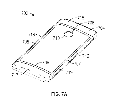
utilizing the transfer of wireless power (e.g., on the order of around one or
multiple
Watts)), as losses may be significantly reduced. Furthermore, the metal back
cover 702
of FIG. 7A has a low resistance while maintaining strong mutual coupling
properties
(e.g., strong mutual inductance) between the transmitter/receiver.
[0071] FIG. 7B
is a diagram of an exploded isometric view of the metal back
cover of FIG. 7A. As shown in FIG. 7B, the top section 715, middle section
716, bottom
section 717, left section 718, and right section 719 are separate from each
other. As
discussed above, the individual sections 715, 716, 717, 718, and 719 may be
held together
by the material filling horizontal slots 704 and 706 and vertical slots 705
and 707 of FIG.
7A. FIG. 7B more clearly shows how the individual sections 715, 716, 717, 718,
and 719
-18-
CA 02951228 2016-12-05
WO 2016/007234
PCT/US2015/033351
may be configured to be distinct and separate pieces and may function as
separate
antennas isolated from each other by the horizontal and vertical slots 704-
707.
[0072]
Additionally, as an example, the middle section 716 of the metal back
cover 702 may affect the magnetic field (i.e., H-field) of the coil/loop
formed by sections
715, 717, 718, and 719. The magnetic field may be strongest at the hole 710
due to
current that flows along the hole. The magnetic field may be constructively
added inside
the hole, generating the strongest magnetic field at the center of the hole.
In some
implementations with different hole 710 shapes, the magnetic field
distributions may
vary. In some implementations, the resistance of the metal back cover 702 (or
the section
716 of the metal back cover 702) may be increased in an area surrounding the
hole 710.
This increase may be due to equipment near the hole 710 being constructed of
metal
and/or being grounded (i.e., the frame/chassis of the camera may be metal and
may be
grounded to a local ground, or a ferrite core of the NFC coil). The increased
resistance in
this area may be caused by the eddy currents generated in metal or ferrite
structures being
exposed to magnetic fields (i.e., a magnetic field being generated by the
coil/loop formed
by sections 715, 717, 718, and 719 when connected to the feed point and
receiving the
current therefrom).
[0073] FIG. 8A
is a diagram of a perspective view of a metal back cover 702
further enlarged and having additional components, in accordance with one
exemplary
implementation. As shown in FIG. 8A, a portion of the metal back cover 702,
including
the top section 715, the top horizontal slot 704, and the vertical slot 708
connecting the
top horizontal slot 704 to the hole 710, is depicted. FIG. 8A also shows
portions of the
right section 719, the vertical slots 705 and 707, the middle section 716, and
the left
section 718. Additionally, FIG. 8 introduces two new components: an inner
trace 810 and
a conductive connection 811. The inner trace 810 is shown as a line running
through the
center of each of the left vertical slot 705, the top horizontal slot 704, and
the right
vertical slot 707. The inner trace 810 may be a conductive element that passes
through
each of the horizontal and vertical slots 704, 705, 706, and 707 (not all
shown in this
figure). The conductive connection 811 is shown connecting the middle section
716 of
the metal back cover 702 to the right section 719 of the metal back cover 702.
In some
implementations, the inner trace 810 may flow through all portions of the
horizontal and
vertical slots 704, 705, 706, and 707.
[0074] In some
implementations, one or more of the inner trace 810 and the
conductive connection 811 may be included in the implementation of FIG. 7A to
improve
-19-
CA 02951228 2016-12-05
WO 2016/007234
PCT/US2015/033351
inductance of the coil created by the periphery of the metal back cover 702
and to
increase design freedom. In some implementations, the inner traces 810 is
installed
within the horizontal and vertical slots 704, 706, 705, and 707. In some
implementations,
the inner trace 810 is connected to one or more of the sections 715, 717, 718,
and 719 of
the periphery of the metal back cover 702 (not shown in this figure). This
connection
between the inner trace 810 and one or more of the sections 715, 717, 718, and
719
effectively connects the inner trace 810 to the coil discussed above formed by
the sections
715, 717, 718, and 719. Connecting the inner trace 810 to the coil formed by
sections
715, 717, 718, and 719 may effectively increase the inductance of the coil by
adding at
least one additional loop or turn. Thus, in some implementations, the
combination of the
inner trace 810 and the coil formed by sections 715, 717, 718, and 719 is at
least a two
turn coil. The first turn may be the loop formed by sections 715, 717, 718,
and 719, and
the second coil being the inner trace 810 around the horizontal and vertical
slots 704-707.
The inner trace 810 may influence the magnetic field generated by the current
flowing
through the coil formed by sections 715, 717, 718, and 719. The presence and
attachment
of the inner trace coil 810 to the coil formed by sections 715, 717, 718, and
719 may
strengthen the magnetic field generated by the coil as opposed to
concentrating the
strongest portion of the magnetic field around the hole 710 as discussed
above. Thus,
inclusion of additional inner traces coupled to the one or more of the
sections 715, 717,
718, and 719 may impact the strength and distribution of the magnetic field
generated by
a current flow through the loop when used as a receive antenna.
[0075] In some
implementations, the inner trace 810 is coupled to the section
716 of the metal back cover 702 as opposed to one of the sections 715, 717,
718, and 719.
Coupling the inner trace 810 to the middle section 716 may provide a common
reference
ground plane for reduction of electromagnetic interference (EMI) or RF de-
sense on all
antennas of the device. In some implementations, the inner trace 810 may
comprise a
plurality of conductive traces that create a plurality of loops around the
section 716 within
the horizontal and vertical slots 704, 705, 706, and 707. The presence of
additional
conductive traces and/or a plurality of loops formed by the inner trace 810
may increase
the impact the inner trace 810 has on the strength and distribution of the
magnetic field.
In some implementations, the location of the connection of the inner trace 810
to the coil
formed by sections 715, 717, 718, and 719 and/or the number of connections
between the
inner trace 810 and the coil formed by sections 715, 717, 718, and 719 may
vary and
multiple contact points can be present. In some implementations, the location
of the
-20-
CA 02951228 2016-12-05
WO 2016/007234
PCT/US2015/033351
connections between the inner trace 810 and the coil formed by sections 715,
717, 718,
and 719 may be influenced by the current distribution, as current may be added
constructively or destructively. As such, in accordance with the
implementations
described herein one or more inner traces and/or connections as just described
may be
selected to control a distribution and a shape of the magnetic field in the
metal back cover
702 when transmitting or receiving power wirelessly.
[0076] In some
implementations, the inner traces 810 may not be disposed
within the horizontal and vertical slots 704-707 and instead be disposed
internal to the
metal back cover 702. In some implementations, the single or multiple turns of
inner
traces 810 may be disposed in or on a circuit board or other configuration
that is not
coplanar with the horizontal and vertical slots 704-707. In some
implementations, the
inner trace 810 may be disposed in a plastic molding in order to increase
inductance or
mutual coupling. For example, the inner trace 810 may be deposited or wired
directly on
a plastic molding or other material that is installed internal to the metal
back cover 702.
[0077] In some
implementations, the conductive connection 811 may connect
the middle section 716 of the metal back cover 702 to at least one of the four
sections of
the coil formed by sections 715, 717, 718, and 719. The FIG. 8A shows the
conductive
connection 811 located at the top right corner of the metal back cover 702,
near the
vicinity of the feed point. In some implementations, the conductive connection
811 may
be located at one or more other points anywhere around the middle section 716
so long as
the conductive connection 811 connects the middle section 716 to one of
sections 715,
717, 718, and 719. In some implementations, the number and location of the
conductive
connections 811 may provide design freedoms for the antennas used for GPS, Wi-
Fi, and
cellular communications, among others. In some implementations, the conductive
connection 811 is accomplished via electrical connections in a circuit board
internal to the
metal back cover 702. In some implementations, the conductive connection 811
comprises an electrical connection external to the metal back cover 702.
Connecting the
middle section 716 to one of the sections 715, 717, 718, and 719 may connect
the
coil/antenna formed by the sections 715, 717, 718, and 719 to the reference
ground and
may allow the coil/antenna formed by the sections 715, 717, 718, and 719 to
use the
reference ground that may be coupled to the middle section 716 of the metal
back cover
702. In some implementations, connecting the middle section 716 to the coil
formed by
sections 715, 717, 718, and 719 may provide for a more stable reference ground
than
-21-
CA 02951228 2016-12-05
WO 2016/007234
PCT/US2015/033351
without the conductive connection 811. In other implementations, the coil
formed by
sections 715, 717, 718, and 719 may not be connected to the middle section
716.
[0078] FIG. 8B
is a diagram of a metal back cover 702 having a reduced
resistance and enables wireless power transfer through the metal back cover
702
efficiently, in accordance with another exemplary implementation. As shown in
FIG. 8B,
the individual sections 715, 718, 717, and 719 are sequentially electrically
coupled via the
plurality of electrical filters 802a-802c. In an implementation, the
electrical filters 802a-
802c includes inductive chokes. The electrical filters 802a-802c may be
configured to
allow current to pass through the electrical coupler based on a frequency of
the current.
For example, top section 715 is electrically and physically coupled to left
section 718 via
electrical filter 802a (e.g., an inductive choke), while left section 718 is
electrically and
physically coupled to bottom section 717 via electrical filter 802b (e.g., an
inductive
choke). Bottom section 717 is electrically and physically coupled to right
section 719 via
electrical filter 802c (inductive choke). Thus, the loop formed by the
sections 715, 718,
717, and 719 described above comprises the plurality of electrical filters
802a-802c
connecting the individual sections 715, 717, 718, and 719. In some
implementations, the
electrical filters 802a-802 may be replaced with other circuitry capable of
acting as a filter
circuit or switch at certain frequencies. In some implementations, the
electrical filters
802a-802c or similar structures may be disposed on a printed circuit board
(PCB) (not
shown in this figure). In some implementations, the electrical filters 802a-
802c may be
disposed directly on the metal back cover section 715, 717, 718, and 719 or
via a flexible
circuit board or other flexible connection. The remaining components depicted
in FIG.
8B are the same as the components identified in FIG. 7A.
[0079] As
discussed briefly above, in some implementations, the individual
sections 715, 717, 718, and 719 may be configured to operate as individual
antennas. In
such implementations, the electrical filters 802a-802c (e.g., inductive
chokes) may
function to isolate the individual sections 715, 717, 718, and 719 from one
another
dependent upon the frequency of current flowing through the electrical filters
802a-802c
or similar structures. For example, at a wireless power frequency of 6.78 MHz,
the
electrical filters 802a-802c may remain in a "closed" state and allow current
to flow
through the electrical filters 802a-802c to each of the connected sections
715, 717, 718,
and 719. Thus, at the wireless power frequency of 6.78 MHz, the electrical
filter 802a
may allow current to flow between top section 715 and left section 718.
Similarly, the
electrical filter 802b may allow current to flow between left section 718 and
bottom
-22-
CA 02951228 2016-12-05
WO 2016/007234
PCT/US2015/033351
section 717. Finally, the electrical filter 802c may allow current to flow
between the
bottom section 717 and the right section 719. However, at higher frequencies,
for
example at GPS or cellular frequencies (both at least in the hundreds of MHz
range), the
electrical filters 802a-802c may restrict current flow. For example, current
generated by
the top section 715 when functioning as a GPS antenna may not flow through
electrical
filter 802a and thus may remain within the top section 715. The flow of
currents between
the sections 715, 717, 718, and 719 may be impeded may be impeded when they
are
generated at frequencies higher than those used in wireless power
transmission.
Accordingly, the top section 715 and the bottom section 717 may remain
isolated from
one another and from the right and left sections 719 and 718, respectively, in
such
implementations. Thus, at the higher GPS and cellular frequencies, for
example, the
individual sections may continue to function as independent antennas for their
respective
frequency bands. These electrical filters 802a-802c or similar structures may
allow for
the reduction of electromagnetic interference or other sensitivities. The
electrical
isolation provided by the electrical filters 802a-802c or similar equipment
may limit
electromagnetic interference or radio frequency de-sense.
[0080] In some
implementations of FIGs. 7-8B, one or more of the sections
715, 717, 718, and 719 may be configured to independently operate as a
discrete antenna,
for example a GPS, cellular, Wi-Fi, or diversity antenna. For example, the top
section
715 may be configured to operate as or in conjunction with a GPS antenna and
may be
electrically coupled to GPS transmitter/receiver circuitry, as discussed in
relation to top
section 615 of FIG. 6A above. The bottom section 717 may be configured to
operate as
or in conjunction with a cellular antenna, similar to the bottom section 617
discussed in
relation to FIG. 6A above. Similarly, the left and right sections 718 and 719,
respectively, may be configured to operate as or in conjunction with
Bluetooth, Wi-Fi, or
diversity antennas. In some implementations, one or more of the sections 715,
717, 718,
and 719, may operate as or in conjunction with an antenna for any of the
purposes
described above (e.g., GPS, cellular, Bluetooth, Wi-Fi, diversity, etc.). In
some
implementations, the middle section 716 may be connected to a reference ground
internal
to the device. In some implementations, the reference ground may be used by
the one or
more antennas (e.g., GPS, cellular, etc.) described above or one or more
circuits described
above. In some implementations, the coil formed by sections 715, 717, 718, and
719 may
not be connected to the reference ground. Accordingly, each of the top section
715, the
left section 718, right section 719, and the bottom section 717 may comprise
one of the
-23-
CA 02951228 2016-12-05
WO 2016/007234
PCT/US2015/033351
transmit antenna 404 or the receive antenna 504 referenced in FIGs. 4 and 5.
The GPS
circuitry, the Wi-Fi circuitry, the diversity circuitry, and the cellular
circuitry (not shown
in this figure) may comprise one or more of the elements and components of
transmit
circuitry 402 or receive circuitry 502 also of FIGs. 4 and 5.
[0081] In some
implementations, the metal back cover 702 and associated
components may operate as receiving circuitry and components in the reverse of
the
functions described above.
Similarly, any of the components discussed above as
comprising components or circuitry of FIG. 4 may similarly comprise components
or
circuitry of FIG. 5. In such implementations, the coil formed by sections 715,
717, 718,
and 719 of the metal back cover 702 may function as a receive coil or antenna,
generating
a current in response to a magnetic field to which the metal back cover 702 is
exposed.
The generated current may then be fed, via the feed point, to receive
circuitry that may
manipulate the generated current to provide wireless power. Similarly, the
remaining
components discussed in relation to FIGs. 6-8B may serve similar purposes as
discussed
above.
[0082] FIG. 8C
is a diagram of an isometric view of the metal back cover
comprising the additional components described in relation to FIG 8A. As shown
in FIG.
8C, the inner trace 810 is embedded within the horizontal and vertical slots
704-707. The
horizontal and vertical slots 704-707 hold the top section 715, the middle
section 716, the
bottom section 717, the left section 718, and the right section 719 together.
[0083] FIG. 8D
is a diagram of an exploded isometric view of the metal back
cover as described in FIG. 8C. As shown in FIG. 8C, the top section 715, the
middle
section 716, the bottom section 717, the left section 718, and the right
section 719 are
separate from each other. As discussed above, the individual sections 715,
716, 717, 718,
and 719 may be held together by the material filling horizontal slots 704 and
706 and
vertical slots 705 and 707 of FIG. 7A-8C. As described in relation to FIGs. 7A-
8C,
vertical slot 708 connects the hole 710 to the top slot 704. FIG. 8D more
clearly shows
how the individual sections 715, 716, 717, 718, and 719 are distinct and
separate pieces
and may function as separate antennas isolated from each other by the
horizontal and
vertical slots 704-707. Additionally, FIG. 8D shows the inner trace 810 as a
distinct
component separate from the material of the slots 704-707, making a continuous
loop
substantially around the periphery of the metal back cover 702.
[0084] FIG. 9A
is a diagram of a metal band configured to operate as a loop
antenna, in accordance with an exemplary implementation. As shown in FIG. 9, a
metal
-24-
CA 02951228 2016-12-05
WO 2016/007234
PCT/US2015/033351
chassis 902 comprises at least one metal ring 904 and a feed 906 of the metal
chassis 902.
The metal ring 904 may not be a continuous ring. The metal ring 904 coupled to
a feed
906. The feed 906 may be configured to couple the metal ring 904 to a source
(i.e., a
transmitter) or sink (i.e., a receiver) (not shown in this figure). In some
implementations,
the metal ring 904 may be configured to generate a magnetic field for the
transfer of
wireless power in response to an AC current flowing through the metal ring
904, the AC
current coming from the feed 906. Thus, the metal ring 904 may be configured
to transfer
wireless power through a metal object. In another implementation, the metal
ring 904 is
configured to act as a receive antenna as described above.
[0085] In some
implementations, the metal ring 904 may also operate as at
least one of a cellular, Wi-Fi, GPS, or diversity antenna. In some
implementations, as
discussed in relation to FIG. 8B, electrical filters such as inductive chokes
(not shown in
this figure) may be used to isolate the metal ring 904 from specific
components or other
antenna circuitry dependent upon frequencies of a current flow through the
metal ring
904. In some implementations, the metal ring 904 may be split into multiple
pieces (not
shown in this figure), and each piece may be configured to operate as or in
conjunction
with at least one of a GPS antenna, a cellular antenna, a Wi-Fi antenna, a
diversity
antenna, or a cellular antenna. However, in order to provide the ability to
receive or
transmit wireless power, the multiple pieces must be connecting into a single
loop or slot
antenna. In some implementations, one or more portions of the device chassis
may be
utilized to connect the one or more pieces into a single loop or slot antenna.
As discussed
above, in some implementations, these portions of the device chassis may be
configured
to function as electrical filters. At frequencies above the 6.78MHz of the
wireless power
range, the connection portions with the chassis may act as the electrical
filters above and
allow each of the multiple pieces to be electrically isolated. When operating
at 6.78MHz
of the wireless power range, the connection portions with the chassis may not
act as the
electrical filters and may allow the portions to operate as the loop antenna
or the slot loop.
[0086] FIG. 9B
is a diagram of the metal band of FIG. 9A configured to
operate as a loop antenna, in accordance with another exemplary
implementation. As
shown in FIG. 9B, the metal ring 904 is shown without the source feed of the
chassis or
any other components of the device. A slot 908 causes the metal ring 904 to be
discontinuous as discussed above. A plurality of slots 908 may be used, as
described
above, to break the metal ring 904 into multiple pieces (not shown in this
figure).
-25-
CA 02951228 2016-12-05
WO 2016/007234
PCT/US2015/033351
[0087] FIG. 10
is a flowchart of an exemplary method 1000 of wirelessly
receiving power via a wireless field. In an implementation, the metal back
cover 702 of
FIGs. 7A-8D may perform the method 1000. In some implementations, the metal
chassis
902 may perform the method 1000.
[0088] At block
1002, power is wirelessly received via a metal cover. The
metal cover may comprise the metal cover 702 of FIGs. 7A-8D. The metal cover
may
comprise an inner portion and an outer portion. The outer portion is
configured to form a
loop around the inner portion of the metal cover 702 (FIG. 7). In some
implementations,
a plurality of slots separates the inner portion and the outer portion. The
plurality of slots
may comprise slots 705-708 of FIGs. 7A-8D. In some implementations, the
plurality of
slots may comprise individual slots on each side of the metal cover that run
orthogonally
to the slots with which they intersect. In some implementations, the
intersecting slots
may not be orthogonal to each other. The outer portion is configured to
inductively
couple power via the magnetic field. For example, the outer portion may be
configured to
form a single or multi turn antenna or coil capable of generating a current
when exposed
to a magnetic field.
[0089] At block
1004, the load is powered or charged based at least in part on
the received power. The load may comprise a wireless power receive circuit (or
other
circuitry configured to receive the current generated by the outer portion.
[0090] FIG. 11
is a flowchart of an exemplary method 1100 of transmitting
wireless power via a wireless field. In an embodiment, the metal back cover
702 of FIGs.
7A-8D may perform the method 1100. In some implementations, the metal chassis
902
may perform the method 1100.
[0091] At block
1102, the method 1100 includes wirelessly transmits power
via a metal cover. The metal cover may comprise the metal back cover 702 of
FIGs. 7A-
8D. The metal cover may comprise an inner portion and an outer portion. The
outer
portion is configured to form a loop around the inner portion of the metal
cover. The
outer portion is configured to inductively couple power via a magnetic field.
In some
implementations, a plurality of slots separates the inner portion and the
outer portion. In
some implementations, the plurality of slots may comprise individual slots on
each side of
the metal cover that run orthogonally to the slots with which they intersect.
In some
implementations, the intersecting slots may not be orthogonal to each other.
The outer
portion loop may be configured to form a single turn antenna or coil capable
of
generating a magnetic field when a current is driven through the outer
portion.
-26-
CA 02951228 2016-12-05
WO 2016/007234
PCT/US2015/033351
[0092] At block
1104, the method 1100 may generate the magnetic field based
on the current received from a power source coupled to the outer portion of
the metal
cover. The power source may comprise a current source or a wireless power
transmit
circuit (or other circuitry configured to generate the current to drive the
outer portion).
[0093] The
various operations of methods described above may be performed
by any suitable means capable of performing the operations, such as various
hardware
and/or software component(s), circuits, and/or module(s). Generally, any
operations
illustrated in the Figures may be performed by corresponding functional means
capable of
performing the operations. For example, a conducting means for partially
housing a
portable electronic device may comprise a metal back cover 702 (FIG. 7). In
addition,
means for inductively coupling power via the magnetic field may include a
receive
antenna 504 (FIG. 5) that may include an outer portion of a metal back cover
702.
Furthermore, means for powering or charging a load may include receive
circuitry 502
(FIG. 5).
[0094] Further
examples of implementations/embodiments of the invention
are defined as follows:
[0095] 1. An
apparatus for wirelessly receiving power via a magnetic field.
The apparatus includes a metal cover including an inner portion and an outer
portion, the
outer portion configured to form a loop around the inner portion of the metal
cover, the
outer portion configured to inductively couple power via the magnetic field.
The
apparatus further includes a receive circuit electrically coupled to the outer
portion and
configured to receive a current from the outer portion generated in response
to the
magnetic field, the receive circuit configured to charge or power a load based
on the
current.
[0096] 2. The
apparatus of example 1, further including a conductive coupler
configured to electrically couple the outer portion to the inner portion.
[0097] 3. The
apparatus of any of the preceding examples, further including a
conductive trace inserted within each of a plurality of slots separating the
inner portion
from the outer portion, the conductive trace configured to substantially form
a second
loop around the inner portion of the metal cover but within the outer portion
of the metal
cover.
[0098] 4. The
apparatus of example 3, wherein the conductive trace within
each of the plurality of slots is electrically coupled to the outer portion.
-27-
CA 02951228 2016-12-05
WO 2016/007234
PCT/US2015/033351
[0099] 5. The
apparatus of example 4, wherein the outer portion forms a first
turn of an inductor and the conductive trace forms a second turn of the
inductor.
[00100] 6. The apparatus of any of the preceding examples, wherein a plurality
of slots separates the outer portion into a plurality of segments, the
plurality of segments
electrically coupled via at least one electrical coupler to form a single loop
of a coil.
[00101] 7. The apparatus of example 6, wherein the at least one electrical
coupler includes an electrical filter.
[00102] 8. The
apparatus of example 7, wherein the electrical filter is
configured to allow the current to pass through the electrical coupler based
on a frequency
of the current.
[00103] 9. The
apparatus of example 7, wherein the electrical filter is
configured to allow the current to pass through the electrical coupler when
the frequency
of the current is substantially 6.78 MHz and is configured prevent the current
from
passing through the electrical coupler at frequencies substantially higher
than 6.78 MHz.
[00104] 10. The
apparatus of any of the examples 7-9, wherein the electrical
filter includes an inductive choke.
[00105] 11. The
apparatus of any of the preceding examples, wherein the
apparatus further includes a resonant circuit including the outer portion and
a capacitor
electrically coupled to the outer portion, the resonant circuit configured to
resonate at the
frequency of the magnetic field.
[00106] 12. The
apparatus of example 1, wherein a plurality of slots separate
the metal cover into the inner portion and the outer portion.
[00107] 13. The
apparatus of example 12, wherein the plurality of slots extend
substantially around a periphery of the metal cover.
[00108] 14. The
apparatus of any of the preceding examples, wherein the loop
forms at least one turn of a coil.
[00109] 15. The
apparatus of any of the preceding examples, wherein the
apparatus includes at least one of a cellular phone, a GPS unit, a watch, a
mobile media
device, a laptop computer, or a key fob.
[00110] 16. The
apparatus of any of the preceding examples, further including
a housing coupled to the metal cover.
[00111] 17. The
apparatus of any of the preceding examples, wherein the metal
cover is configured as a metal back cover of a portable electronic device.
-28-
CA 02951228 2016-12-05
WO 2016/007234
PCT/US2015/033351
[00112] 18. The
apparatus of example 1, wherein the outer portion includes a
metal ring including at least one slot, the at least one slot configured to
make the metal
ring discontinuous at least one location.
[00113] 19. The
apparatus of any of the preceding examples, wherein the inner
portion functions as a reference ground to the outer portion.
[00114] 20. The apparatus of any of the preceding examples, wherein a first
resistance of the metal cover including the inner and outer portions in
response to the
magnetic field is reduced from a second resistance of a metal cover without
inner and
outer portions.
[00115] 21. A method for wirelessly receiving power via a magnetic field. The
method includes wirelessly receiving power via a metal cover including an
inner portion
and an outer portion, the outer portion configured to form a loop around the
inner portion
of the metal cover, the outer portion configured to inductively couple power
via the
magnetic field. The method further includes powering or charging a load based
on the
received power.
[00116] 22. The method of example 21, wherein wirelessly receiving power via
the metal cover further includes wirelessly receiving power via the metal
cover further
including a conductive trace inserted within each of a plurality of slots
separating the
outer portion from the inner portion, the conductive trace configured to
substantially form
a second loop around the inner portion of the metal cover but within the outer
portion of
the metal cover, the conductive trace electrically coupled to the outer
portion.
[00117] 23. The method of example 21, wherein a plurality of slots separate
the
outer portion into a plurality of segments and wherein the plurality of
segments are
electrically coupled to each other via at least one electrical coupler to form
a single loop
antenna.
[00118] 24. The method of example 23, wherein the at least one electrical
coupler includes an electrical filter.
[00119] 25. The method of example 24, wherein the method further includes
selectively allowing current to pass through the electrical coupler based on a
frequency of
the current via the electrical filter.
[00120] 26. The method of example 25 wherein selectively allowing current to
pass through the electrical coupler based on the frequency includes allowing
the current
to pass through the electrical coupler when the frequency of the current is
substantially
-29-
CA 02951228 2016-12-05
WO 2016/007234
PCT/US2015/033351
6.78 MHz and preventing the current from passing through the electrical
coupler at
frequencies substantially higher than 6.78 MHz.
[00121] 27. The method of any of examples 21-26, wherein the metal cover is
part of at least one of a cellular phone, a GPS unit, a watch, a mobile media
device, a
laptop computer, or a key fob.
[00122] 28. The method of any of examples 21-27, wherein a housing is
coupled to the metal cover.
[00123] 29. The method of example 21, wherein a plurality of slots separate
the
metal cover into the inner portion and the outer portion.
[00124] 30. The method of any of examples 21-29, wherein the inner portion
functions as a reference ground to the outer portion.
[00125] 31. The method of any of examples 21-30, wherein a first resistance of
the metal cover including the inner and outer portions in response to the
magnetic field is
reduced from a second resistance of a metal cover without inner and outer
portions.
[00126] 32. An apparatus for receiving wireless power from a magnetic field.
The apparatus includes conducting means for partially housing a portable
electronic
device, the conducting means including an inner portion and an outer portion,
the outer
portion configured to form a loop around the inner portion of the conducting
means, the
outer portion including means for inductively coupling power via the magnetic
field. The
apparatus further includes means for powering or charging a load based on
power
receiving via the outer portion.
[00127] 33. An apparatus for wirelessly receiving power. The apparatus
includes a housing portion configured to form a back of a portable electronic
device, the
housing portion having a first dimension. The housing portions includes a
metal portion
having a second dimension the same size as or having a size that covers a
majority of the
first dimension of the housing portion, at least a portion of the metal
portion configured to
inductively couple power via a magnetic field at a level sufficient for
charging or
powering a load of the portable electronic device. The apparatus further
includes an
electrical connection electrically coupled to the metal portion and configured
to provide
received power to the portable electronic device.
[00128] 34. The apparatus of example 33, wherein the metal portion is
configured to generate current in response to a voltage induced by the
magnetic field
generated by a transmitter.
-30-
CA 02951228 2016-12-05
WO 2016/007234
PCT/US2015/033351
[00129] 35. The apparatus of any of examples 33-34, wherein the metal portion
includes an inner portion and an outer portion, the outer portion configured
to form a loop
around the inner portion of the metal portion forming at least one turn of a
coil configured
to inductively couple the power via the magnetic field.
[00130] Information and signals may be represented using any of a variety of
different technologies and techniques. For example, data, instructions,
commands,
information, signals, bits, symbols, and chips that may be referenced
throughout the
above description may be represented by voltages, currents, electromagnetic
waves,
magnetic fields or particles, optical fields or particles, or any combination
thereof
[00131] The
various illustrative logical blocks, modules, circuits, and algorithm
steps described in connection with the implementations disclosed herein may be
implemented as electronic hardware, computer software, or combinations of
both. To
clearly illustrate this interchangeability of hardware and software, various
illustrative
components, blocks, modules, circuits, and steps have been described above
generally in
terms of their functionality. Whether such functionality is implemented as
hardware or
software depends upon the particular application and design constraints
imposed on the
overall system. The described functionality may be implemented in varying ways
for each
particular application, but such implementation decisions may not be
interpreted as
causing a departure from the scope of the implementations of the invention.
[00132] The
various illustrative blocks, modules, and circuits described in
connection with the implementations disclosed herein may be implemented or
performed
with a general purpose processor, a Digital Signal Processor (DSP), an
Application
Specific Integrated Circuit (ASIC), a Field Programmable Gate Array (FPGA) or
other
programmable logic device, discrete gate or transistor logic, discrete
hardware
components, or any combination thereof designed to perform the functions
described
herein. A general purpose processor may be a microprocessor, but in the
alternative, the
processor may be any conventional processor, controller, microcontroller, or
state
machine. A processor may also be implemented as a combination of computing
devices,
e.g., a combination of a DSP and a microprocessor, a plurality of
microprocessors, one or
more microprocessors in conjunction with a DSP core, or any other such
configuration.
[00133] The steps of a method or algorithm and functions described in
connection with the implementations disclosed herein may be embodied directly
in
hardware, in a software module executed by a processor, or in a combination of
the two.
If implemented in software, the functions may be stored on or transmitted over
as one or
-31-
CA 02951228 2016-12-05
WO 2016/007234
PCT/US2015/033351
more instructions or code on a tangible, non-transitory computer-readable
medium. A
software module may reside in Random Access Memory (RAM), flash memory, Read
Only Memory (ROM), Electrically Programmable ROM (EPROM), Electrically
Erasable
Programmable ROM (EEPROM), registers, hard disk, a removable disk, a CD ROM,
or
any other form of storage medium known in the art. A storage medium is coupled
to the
processor such that the processor may read information from, and write
information to,
the storage medium. In the alternative, the storage medium may be integral to
the
processor. Disk and disc, as used herein, includes compact disc (CD), laser
disc, optical
disc, digital versatile disc (DVD), floppy disk and Blu-ray disc where disks
usually
reproduce data magnetically, while discs reproduce data optically with lasers.
Combinations of the above may also be included within the scope of computer
readable
media. The processor and the storage medium may reside in an ASIC.
[00134] For purposes of summarizing the disclosure, certain aspects,
advantages and novel features of the inventions have been described herein. It
is to be
understood that not necessarily all such advantages may be achieved in
accordance with
any particular implementation of the invention. Thus, the invention may be
embodied or
carried out in a manner that achieves or optimizes one advantage or group of
advantages
as taught herein without necessarily achieving other advantages as may be
taught or
suggested herein.
[00135] Various modifications of the above described implementations will be
readily apparent, and the generic principles defined herein may be applied to
other
implementations without departing from the spirit or scope of the invention.
Thus, the
present invention is not intended to be limited to the implementations shown
herein but is
to be accorded the widest scope consistent with the principles and novel
features
disclosed herein.
-32-