Note: Descriptions are shown in the official language in which they were submitted.
275879
LED PACKAGE WITH RED-EMITTING PHOSPHORS
FIELD
[0000] The present invention relates to process for fabricating a LED
lighting
apparatus.
BACKGROUND
[0001] Red-emitting phosphors based on complex fluoride materials
activated by
Mn4+, such as those described in US 7,358,542, US 7,497,973, and US 7,648,649,
can be utilized in combination with yellow/green emitting phosphors such as
YAG:Ce
or other garnet compositions to achieve warm white light (CCTs<5000 K on the
blackbody locus, color rendering index (CRI) >80) from a blue LED, equivalent
to that
produced by current fluorescent, incandescent and halogen lamps. These
materials
absorb blue light strongly and efficiently emit between about 610-635 nm with
little
deep red/NIR emission. Therefore, luminous efficacy is maximized compared to
red
phosphors that have significant emission in the deeper red where eye
sensitivity is
poor. Quantum efficiency can exceed 85% under blue (440-460 nm) excitation.
[0002] While the efficacy and CRI of lighting systems using Mn4+ doped
fluoride
hosts can be quite high, one potential limitation is their susceptibility to
degradation
under use conditions. It is possible to reduce this degradation using post-
synthesis
processing steps, as described in US 8,252,613. However, development of
alternative methods for improving stability of the materials is desirable.
BRIEF DESCRIPTION
[0003] Briefly, in one aspect, the present invention relates to a
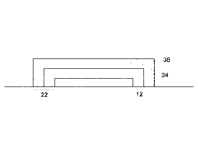
process for
fabricating a LED lighting apparatus including disposing a composite coating
on a
surface of a LED chip. The composite coating includes first composite layer
having a
manganese doped phosphor of formula I and a first binder, and a second
composite
layer having a second phosphor composition and a second binder. The first
binder,
the second binder or both comprise a poly(meth)acrylate.
Ax [MFy]:Mn4+ .................. (I)
wherein
A is Li, Na, K, Rb, Cs, or a combination thereof;
M is Si, Ge, Sn, Ti, Zr, Al, Ga, In, Sc, Hf, Y, La, Nb, To, Bi, Gd, or a
combination thereof;
x is the absolute value of the charge of the [MFy] ion;
1
Date recue/ date received 2022-02-17
CA 02951381 2016-12-06
WO 2015/191521
PCT/US2015/034818
y is 5,6 or 7.
[0004] In another aspect, a LED lighting apparatus according to the present
invention includes a composite coating disposed on a LED chip. The composite
coating includes first composite layer having a manganese doped phosphor of
formula I and a first binder, and a second composite layer having a second
phosphor
composition and a second binder. The first binder, the second binder or both
comprise a poly(meth)acrylate.
DRAWINGS
[0005] These and other features, aspects, and advantages of the present
invention will become better understood when the following detailed
description is
read with reference to the accompanying drawings in which like characters
represent
like parts throughout the drawings, wherein:
[0006] FIG. 1 is a schematic cross-sectional view of a lighting apparatus
according to the present invention.
[0007] FIG. 2 is a schematic cross-sectional view through a composite
coating
according to one embodiment of the present invention.
[0008] FIG. 3A shows cross-sectional view of a configuration of a composite
coating disposed on a LED chip according to one embodiment of the present
invention.
[0009] FIG. 3B shows cross-sectional view a configuration of a composite
coating disposed on a LED chip according to another embodiment of the present
invention.
[0010] FIG. 4 shows emission spectra of two configurations of the composite
coating shown in FIGS. 3A and 38.
DETAILED DESCRIPTION
(0011] Approximating language, as used herein throughout the specification
and
claims, may be applied to modify any quantitative representation that could
permissibly vary without resulting in a change in the basic function to which
it is
related. Accordingly, a value modified by a term or terms, such as "about," is
not
CA 02951381 2016-12-06
WO 2015/191521
PCT/US2015/034818
limited to the precise value specified. In some instances, the approximating
language may correspond to the precision of an instrument for measuring the
value.
In the following specification and claims, the singular forms "a". "an" and
"the" include
plural referents, unless the context clearly dictates otherwise.
[0012] Unless defined otherwise, technical and scientific terms used herein
have
the same meaning as is commonly understood by one of skill in the art to which
this
invention belongs. The terms "first", "second", and the like, as used herein
do not
denote any order, quantity, or importance, but rather are used to distinguish
one
element from another.
[0013] In the present disclosure, when a layer is being described as "on"
another
layer or substrate. it is to be understood that the layers can either be
directly
contacting each other or have one (or more) layer or feature between the
layers.
Further, the term "on" describes the relative position of the layers to each
other and
does not necessarily mean "on top of' since the relative position above or
below
depends upon the orientation of the device to the viewer. Moreover, the use of
"top."
"bottom," "above," "below,' and variations of these terms is made for
convenience,
and does not require any particular orientation of the components unless
otherwise
stated. The term "adjacent" as used herein means that the two layers are
disposed
contiguously and are in direct contact with each other.
[0014] A cross sectional view of a lighting apparatus or light emitting
assembly or
lamp 10 according to one embodiment of the present invention is shown in FIG.
1.
Lighting apparatus 10 includes a semiconductor radiation source, shown as
light
emitting diode (LED) chip 12, and leads 14 electrically attached to the LED
chip. The
leads 14 may be thin wires supported by a thicker lead frame(s) 16 or the
leads may
be self-supported electrodes and the lead frame may be omitted. The leads 14
provide current to the LED chip 12 and thus cause it to emit radiation.
[0015] The lamp may include any semiconductor blue or UV light source that
is
capable of producing white light when its emitted radiation is directed onto
the
phosphor. In one embodiment, the semiconductor light source is a blue emitting
LED
doped with various impurities. In one embodiment, the LED may contain at least
one
semiconductor layer comprising GaN, ZnSe, or SIC. In particular, the
semiconductor
light source may be a blue emitting LED semiconductor diode based on a nitride
compound semiconductor of formula IniGaiAlkN (where 05.i: 05j; 05.k and I + j
+ k =1)
3
CA 02951381 2016-12-06
WO 2015/191521
PCT/US2015/034818
having an emission wavelength greater than about 250 nm and less than about
550
nm. More particularly, the LED chip 12 (FIG. 1) may be a near-UV or blue
emitting
LED having a peak emission wavelength from about 400 to about 500 nm. Such
LED semiconductors are known in the art. The radiation source is described
herein
as a LED for convenience. However, as used herein, the term is meant to
encompass all semiconductor radiation sources including, e.g., semiconductor
laser
diodes. Further, although the general discussion of the exemplary structures
of the
invention discussed herein is directed toward inorganic LED based light
sources, it
should be understood that the LED chip may be replaced by another radiation
source
unless otherwise noted and that any reference to semiconductor, semiconductor
LED, or LED chip is merely representative of any appropriate radiation source,
including, but not limited to, organic light emitting diodes.
[0016] In lighting apparatus 10. a composite coating 22 is disposed on a
surface
of LED chip 12. The composite coating 22 includes a first composite layer and
a
second composite layer, each composite layer having at least one phosphor
composition. In one instance, the phosphor compositions are radiationally
coupled to
the LED chip 12. Radiationally coupled means that the elements are associated
with
each other so that the radiation from one is transmitted to the other. For
example,
the composite coating 22 is disposed on the LED chip 12 such as a radiation
from
LED chip 12 is transmitted to the phosphors, and the phosphors emit radiation
of
different wavelengths.
[0017] In a particular embodiment, the LED chip 12 is a blue LED, and the
first
composite layer includes the red line emitting phosphor of formula I and the
second
composite layer includes a yellow-green phosphor such as a cerium-doped
yttrium
aluminum garnet, Ce:YAG. The blue light emitted by the LED chip 12 mixes with
the
red and yellow-green light emitted respectively by the phosphors of the first
composite layer and the second composite layer, and the resulting emission
(indicated by arrow 24) appears as white light.
[0018] LED chip 12 may be enclosed by an encapsulant material 20. The
encapsulant material 20 may be a low temperature glass, or a thermoplastic or
thermoset polymer or resin as is known in the art, for example, a silicone or
epoxy
resin. LED chip 12 and encapsulant material 20 may be encapsulated within a
shell
18. Both the shell 18 and the encapsulant 20 should be transparent to allow
white
light 24 to be transmitted through those elements. In some embodiments, the
4
CA 02951381 2016-12-06
WO 2015/191521
PCT/US2015/034818
encapsulant material may form the shell 18. In addition, scattering particles
may be
embedded in the encapsulant material. The scattering particles may be, for
example,
alumina or titania. The scattering particles effectively scatter the
directional light
emitted from the LED chip, preferably with a negligible amount of absorption.
[0019] In an alternate embodiment, the lamp 10 may only include an
encapsulant
material without an outer shell 18. The LED chip 1 may be supported, for
example.
by the lead frame 16, by the self-supporting electrodes, the bottom of shell
18 or by a
pedestal (not shown) mounted to shell 18 or to the lead frame.
[0020] The manganese (Mn4")-doped phosphor of formula I is a red line
emitting
manganese (Mn4+)-doped complex fluoride phosphor. In the context of the
present
invention, the term "complex fluoride material or phosphor", means a
coordination
compound, containing at least one coordination center, surrounded by fluoride
ions
acting as ligands, and charge-compensated by counter ions as necessary. In one
example, K2SiF6:Mn44., the coordination center is Si and the counterion is K.
Complex fluorides are occasionally written down as a combination of simple,
binary
fluorides but such a representation does not indicate the coordination number
for the
ligands around the coordination center. The square brackets (occasionally
omitted
for simplicity) indicate that the complex ion they encompass is a new chemical
species, different from the simple fluoride ion. The activator ion (Me) also
acts as a
coordination center, substituting part of the centers of the host lattice, for
example,
Si. The host lattice (including the counter ions) may further modify the
excitation and
emission properties of the activator ion.
[0021] In particular embodiments, the coordination center of the phosphors,
that
is, M in formula I, is Si, Ge, Sn, Ti, Zr, or a combination thereof. More
particularly,
the coordination center is Si, Ge, Ti, or a combination thereof, and the
counterion, or
A in formula I, is Na, K, Rb, Cs, or a combination thereof, and y is 6.
Examples of
precursors of formula I include K2[SiF6]:Mn4+, K2[TiFEJ:Mn4., K2[SnF6]:Mn4
s
Cs2[TiF6]:Me, Rb2[TiF6]:Mn4+, Cs2[SiFij:Mn4+, Rb2[SiF6):Mn4+, Na2[TiF6]:Mn4+,
Na2[ZrE61:Me, K3[ZrF7]:Mn4., K3[BiE]:Mn4t. K3[YF6]:Mn4f, K3[LaF6]:Mn4",
K3[GdF6]:Mn4f, K3[NbF7]:Mn4-, K3[TaF7]:Mn4'. In particular embodiments, the
precursor of formula I is K2SiF6:Me.
[0022] In one embodiment, the Mn'-doped phosphor is selected from the group
consisting of
CA 02951381 2016-12-06
WO 2015/191521
PCT/US2015/034818
(A) A2[MF]:Mn4`, where A is selected from Li, Na, K, Rb, Cs, and combinations
thereof; and where M is selected from Al, Ga, In, and combinations thereof;
(B)A3[MF6]:Me, where A is selected from Li, Na, K, Rb, Cs, and combinations
thereof; and where M is selected from Al, Ga, In, and combinations thereof;
(C) Zn2[MF7]:Mn4 , where M is selected from Al, Ga, In, and combinations
thereof;
(D)A[In2F7]:Mn4+ where A is selected from Li, Na, K. Rb, Cs, and combinations
thereof;
(E)A2[MF6]:Mn4+, where A is selected from Li, Na, K, Rb, Cs, and combinations
thereof; and where M is selected from Ge, Si, Sn, Ti, Zr, and combinations
thereof;
(F) E[MF6]:Me. where E is selected from Mg, Ca, Sr, Ba, Zn, and combinations
thereof; and where M is selected from Ge, Si, Sn, Ti, Zr, and combinations
thereof;
(G) Ba065Zr0.35F2.70:Me; and
(H) A3[ZrF7i:Mn4+ where A is selected from Li, Na, K, Rb, Cs, and combinations
thereof.
(0023] The amount of manganese in the Me doped precursors of formula I and
groups (A)-(H), and in the product phosphors ranges from about 0.3 weight%
(wt%)
to about 2.5 wt%, (from about 1.2 mole % (mol%) to about 10 mol%), based on
total
weight of the precursor or the phosphor. In some embodiments, the amount of
manganese ranges from about 0.3 wt% to about 1.5 wt% (from about 1.2 mol% to
about 6 mol%), particularly from about 0.50 wt% to about 0.85 wt% (from about
2
mol% to about 3.4 mol%), and more particularly from about 0.65 wt% to about
0.75
wt% (from about 2.6 mol% to about 3 mol%). In other embodiments, the amount of
manganese ranges from about 0.75 wt% to about 2.5 wt% (about 3 m01% to about
mol%), particularly from about 0.9 wt% to about 1.5 wt% (from about 3.5 mol%
to
about 6 mol%), more particularly from about 0.9 wt% to about 1.4 wt% (about
3.0
mol% to about 5.5 mol%), and even more particularly from about 0.9 wt% to
about
1.3 wt% (about 3.5 mol% to about 5.1 mol%).
[0024] The Mn" doped phosphors may have a population of particles having a
particle size distribution with a 050 value in a range from about 10 micron to
about
80 microns. The phosphor materials described herein are commercially
available, or
6
CA 02951381 2016-12-06
WO 2015/191521
PCT/US2015/034818
prepared by methods as known in the art, e.g., through solid-state reaction
methods
by combining, for example, elemental oxide, carbonates, and /or hydroxides as
starting material. In some embodiments, it is desirable to use particles of
small
particle size, for example a D50 particle size of less than about 30 microns.
In
particular embodiments, the D50 particle size of the particles ranges from
about 10
microns to about 20 microns, and more particularly from about 12 microns to
about
18 microns. In some embodiments, the particles of the Mn4+ doped phosphors are
post-treated for enhancing performance and color stability of the resulting
phosphors
as described in US Patent No. 8,252,613.
[0025] FIG. 2 is a cross section view of a composite coating 22 (also
referred to
as 'laminate") showing that composite coating 22 is composed of at least two
layer; a
first composite layer 34 and the second composite layer 36. The first
composite
layer 34 includes a manganese doped phosphor of formula I and a first binder.
The
second composite layer 36 includes a second phosphor (an additional phosphor)
and
a second binder. The second phosphor is a phosphor composition that emits a
radiation which produces white light in combination with the emissions of the
first
composite layer 34 and the LED chip 12 (FIG. 1), which are described in detail
below.
[0026] In one embodiment, a phosphor composition is interspersed in a
binder
material within a composite layer. The phosphor composition may be mixed with
a
binder material (or a binder) to form a composite phosphor material, which can
be
subsequently pressed to form a composite layer or film. The composite phosphor
material may include the phosphor composition in the form of powder, and the
binder
material as a matrix. The matrix or the binder material may be an encapsulant
material. Suitable examples of the binder materials may be a low temperature
glass,
or a thermoplastic or thermoset polymer or a resin as is known in the art, for
example, a silicone or epoxy resin.
[0027] In one embodiment, the phosphor of formula I is mixed with a first
binder
and the mixture is heated and pressed to form the first composite layer 34. In
one
embodiment, the second phosphor is mixed with a second binder; and then heated
and pressed to form the second composite layer 36. Both the first binder and
the
second binder should be transparent to the light emitted from the LED and the
phosphors. In one embodiment, the first binder, the second binder, or both
have a
glass transition temperature (T9) higher than the operating temperature of the
LED
7
CA 02951381 2016-12-06
WO 2015/191521
PCT/US2015/034818
chip. According to one embodiment of the invention, the first binder, the
second
binder or both are a poly(meth)acrylate polymer or copolymer. A suitable
poly(meth)acrylate binder includes, but is not limited to, poly(methyl
methacrylate)
(PMMA). Many polymer and copolymer formulations derived from (meth)acrylic
acid
and (meth)acrylate ester monomers may be used for the binder. In some
embodiments, both the first binder and the second binder are (meth)acrylates.
In
some embodiments, the second binder may be a different material from that of
the
first binder. Suitable examples of a different binder material may include,
but are not
limited to, mono and copolymers obtained from materials such as
polycarbonates,
cyclic olefins, polysulfones, polyesters, polystyrene, polyproplyene and
fluorplastic
resins.
[0028] In some embodiments, the binder material (the first binder or the
second
binder) has an index of refraction R, and contains a diluent material having
less than
about 5% absorbance and index of refraction of R 0.1. The diluent material
has an
index of refraction of 51.7, particularly 51.6, and more particularly 51.5. In
a
particular embodiment, the diluent material is of formula AAMFO, and has an
index of
refraction of about 1.4. Adding an optically inactive material to the
phosphor/binder
mixture may produce a more gradual distribution of light flux through the
phosphor/encapsulant mixture and can result in less damage to the phosphor.
Suitable materials for the diluent include fluoride compounds such as LiF,
M9F2,
CaF2, SrF2, AlF3, K2NaAlF6, kMgF3, CaLiAlF6, K2LiAlF6, and K2SiF6, which have
index
of refraction ranging from about 1.38 (AlFsand K2NaAlF6) to about 1.43 (CaF2),
and
polymers having index of refraction ranging from about 1.254 to about 1.7. Non-
limiting examples of polymers suitable for use as a diluent include
polycarbonates,
polyesters, nylons, polyetherimides, polyetherketones, and polymers derived
from
styrene, acrylate, methacrylate, vinyl, vinyl acetate, ethylene, propylene
oxide, and
ethylene oxide monomers, and copolymers thereof, including halogenated and
unhalogenated derivatives. These polymer powders can be directly incorporated
into
the binder materials, for example acrylates before curing.
[0029] During pressing, the composite phosphor materials are heated at
least up
to their respective melting temperatures. In one embodiment, the heating
temperature may range from about 150 C to about 200 C. On heating, the binder
materials soften; and the phosphor materials intersperse within the respective
molten
8
275879
binders to form, respectively, the first composite layer 34 and the second
composite
layer 36.
[0030] These separately formed layers, the first composite layer 34 and
the
second composite layer 36, are subsequently disposed one over another, and
bonded to form the composite coating 22. In one embodiment, the first
composite
layer 34 substantially covers the second composite layer 36 such that the
light
emitted by one of the layers passes through another layer. In some
embodiments,
the first composite layer 34 and the second composite layer 36 are cured to
bond the
two layers. During curing, the binder materials diffuse at the interface of
the two
layers 34 and 36, and form a bond (joint) between the two layers. Alternately,
an
adhesive can be used to join the two layers. The resulting composite coating
22 is
then disposed on the LED chip 12. In some instances, a polymer layer or a
silicone
layer (not shown) can be used to adhere the composite coating 22 to the chip.
In
some embodiments, the composite coating 22 is arranged remotely in the
vicinity of
the LED chip 12.
[0031] The laminate or the composite coating can be molded in distinct
shapes
which can be placed directly over a LED on a board package or can be diced and
placed on a LED package. One embodiment is a chip-scale package.
[0032] As mentioned above, the phosphor material (in the form of a
powder) is
interspersed in the binder material within the composite layer. The phosphor
may be
interspersed within a single region or particular regions of the layer, or
throughout the
entire volume of the binder material in the layer. The distribution of the
phosphor
material within the layer can be controlled by selecting particulates of the
binder
material of a suitable particle size. The particulates of the binder material
may have
a particle size distribution with a D50 value less than about 300 microns. In
one
embodiment, the particulates have a D50 particle size in a range from about
150
microns to about 300 microns. In one embodiment, smaller particulates, for
example
having D50 particle size less than about 50 microns, are desirable. In one
embodiment, the binder particulates have a D50 particle size in a range from
about
20 microns to about 50 microns.
[0033] The particle size of a binder material may be tailored to adjust
the spacing
between the phosphor particles in the composite layer. Using a large binder
particulate size may result in large spacing among phosphor particles and high
forward scattering of the LED emitted light. This may be accomplished mixing
the
9
Date recue/ date received 2022-02-17
CA 02951381 2016-12-06
WO 2015/191521
PCT/US2015/034818
phosphor with the binder at a temperature that is approximately the melting
temperature of the binder. Since the viscosity of the polymer is high at this
temperature, little or no dispersion (mixing or settling) of the phosphor
particles
occurs. Using small binder particle size may result in closely packed phosphor
particles and less forward scattering with high absorption.
[0034] Referring to FIG. 1 again, blue light emitted by the LED chip 12
mixes with
the light emitted by the first composite layer 34 and the second composite
layer 36
(FIG. 2) of the composite coating 22, and the mixed light appears as white
light. By
controlling the particle size and/or distribution of particles (as discussed
above) of the
first and second phosphors, the binder materials or both prior to pressing
into the first
composite layer 34 and the second composite layer 36, the light emission from
the
individual layers can be tuned to produce desired color point.
[0035] In addition, the light emission can further be tuned by controlling
the
location (closer or farther from the LED chip 12) of the first phosphor and
the second
phosphor. FIGS. 3A and 3B show cross sectional views through LED chip 12
having
the composite coating 22 disposed on the chip 12, depicting two
configurations. In
FIG 3A, the composite coating 22 is disposed on the LED chip 12 such as to
place
the first composite layer 34 containing manganese doped phosphor of formula I,
close (adjacent) to the LED chip 12. That is, in this configuration, the
composite
coating 22 is disposed on the LED chip 12 with the first composite layer 34
side
disposed on the chip. In FIG. 3B, the composite coating 22 is disposed on the
LED
chip 12 with the second composite layer 36 disposed adjacent (down) to the LED
chip 12, and the first composite layer 34 side (containing PFS) farther from
the LED
chip 12. For example, FIG. 4 and Table 1 show spectral characteristics of the
two
LED-based lamps, one having PFS-containing layer side disposed on the chip
(PFS
down) and another having YAG-containing layer side disposed on the chip (YAG
down). These exemplary lamps and corresponding results are described in detail
below in the example section.
[0036] Moreover, the first composite layer 34 containing the phosphor of
formula
I, may have a graded composition of the phosphor of formula I as described in
U.S.
Patent Application Serial No. 14/073141 filed on November 6, 2013. The
composition of the phosphor of formula I vary in one or more of manganese
concentration, density of particles, or particle size across a thickness
thereof, that is
in a direction normal to the plane of the surface of the LED chip 12. In one
CA 02951381 2016-12-06
WO 2015/191521
PCT/US2015/034818
embodiment, the manganese concentration ranges from a minimum value in a
region
proximate to the LED chip 12 to a maximum value in a region opposite to the
LED
chip 12. In one embodiment, the density of particles of the first population
is greater
than density of particles of the second population. In one embodiment, the D50
particle size of the first population of particles is greater than the D50
particle size of
the second population of particles.
[0037] The phosphor particles may be disposed in a band structure, where a
first
population of particles is located generally in a region of the first
composite layer 34
proximate to the LED chip and a second population of particles generally
located in a
region opposite to the LED chip. In some instances, the first composite layer
34
includes two separate layers disposed one over another; one having the first
population of particles and another having a second population of particles.
The first
composite layer 34 may not have a distinct interface at which the composition
changes abruptly. Particles of the first population may be mixed with
particles of the
second population throughout the first composite layer 34; however, in all of
these
embodiments, the layer 34 has a graded composition varying in one or more of
manganese concentration, density of particles, or particle size.
[0038] In combination with the Mn4+ doped phosphor and the second phosphor
in
the second composite layer 36, the LED chip produces resulting emissions with
color
point, color temperature, or color rendering as desired. When used in a
lighting
apparatus in combination with a blue or near UV LED emitting radiation in the
range
of about 250 to 550 nm, the resultant light emitted by the assembly will be a
white
light. The second phosphor may include a green, yellow, blue, red, orange, or
other
color phosphors that can be used in combination with the phosphor of formula I
to
customize the white color of the resulting light and produce specific spectral
power
distributions. In some instances, multiple composite layers, each including at
least
one phosphor composition, may be used to form the composite coating.
[0039] The green or yellow emitting phosphor materials may include one or
more
of europium doped or cerium doped rare earth oxides or oxynitride phosphors.
More
particularly, the second phosphor is a phosphor that emits yellow-green light
upon
excitation by the LED chip, for example a Ce-doped '(AG.
(Y,Gd,Tb,La,Sm,Pr,Lu)3(AI,Ga)5.x012-3/2.:Ce31 (wherein 0cx50.5).
II
CA 02951381 2016-12-06
WO 2015/191521
PCT/US2015/034818
[00401 Other suitable phosphors for use along with the phosphor of fomiula
I
include, but are not limited to:
((Sri,. (Ca, Ba, Mg, Zn),),..0õ.,õõ)( Li, Na, K, Rb)õCe,)3(AySiy)04,-y+3(x-
w)Fi-y-3ix-w),
0<x5Ø10, 0.5.y5Ø5, 05.z5Ø5, 0.5.w5x;
(Ca, Ce)3Sc2Si3012 (CaSiG);
(Sr,Ca,Ba)3A11Six04"Fl.,,:Ce3+ (SASOF));
(Ba,Sr,Ca)5(PO4)3(CI,F,8r,OH):Eu2+,Mn2 ; (Ba,Sr,Ca)BP05:Ee,Mn2+;
(Sr,Ca)10(PO4)6*03203:Eu2+ (wherein 0<v5.1); Sr2Si308*2SrCl2:Eu2+;
(Ca,Sr,Ba)3MgSi208:Eu2',Mn2'; 8aA18013:Eu2'; 2SrO*0.84P205*0.168203:Eu2I;
(Ba,Sr,Ca)MgA110017:Eu2",Mn2'; (Ba,Sr,Ca)A1204:Eu2.;
(Y,Gd,Lu,Sc,La)B03:Ce3',Tb3+;
ZnS:Cu ,CI-; ZnS:Cu+,A13+; ZnS:Ag+,Cr; ZnS:Ag+,A13 ;
(Ba,Sr,Ca)2Si1.,:04.2z,:Eu2+
(wherein 0.25450.2); (Ba,Sr,Ca)2(Mg2n)S1207:Eu2+;
(Sr,Ca,Ba)(AI,Ga,ln)2S4:Eu2+;
(Y,Gd,Tb,La,Sm,Pr,Lu)3(AI,Ga).5õ.012-3:2,:Ce3 (wherein 050E50.5);
(Ca,Sr)8(Mg,Zn)(SiO4)4C12:Eu2+,Mn21; Na2Gd2B207:Ce31.,Tb3E;
(Sr,Ca,Ba,Mg,Zn)2P207:Eu2+,Mn2'; (Gd,Y,Lu,La)203:Eu3-,Bi3+;
(Gd,Y,Lu,La)202S:Eu3+,Bi3'; (Gd,Y,Lu,La)1/04:Eu3+,B13 ; (Ca,Sr)S:Eui+,Ce3+;
SrY2S4:Eu2'; CaLa2S4:Ce3f; (Ba,SrsCa)MgP207:Eu2',Mn2+; (Y,Lu)2W06:Eu3+,Mo6+;
(Ba,Sr,Ca)pSiyNõ:Eu2- (wherein 28+47=30; (Ba,Sr,Ca)2SiAI3Ng.,03:Eu21(wherein
0)<2); Ca3(SiO4)C12:Eu2+;
(Lu,Sc,Y,Tb)2.,,..,Ce,Cal.,,LiwMg24,P,õ(Si,Ge)3õ012.,,2 (where
-0.5sus1, 0<v50.1, and 05.w5Ø2); (Y,Lu,Gd)2..2C;Si4N6.õC1õ:Ce31, (wherein
05(1)50.5); (Lu,Ca,Li,Mg,Y), a-SiAION doped with Eu2+ and/or Ce3+;
(Ca,Sr,Ba)SiO2N2:Eu2',Ce3'; i3-Si1AION:Eu2+.3.5MgO*0.5MgF2*Ge02:Mnd+;
(Sr,Ca,Ba)AlSiN3:Eu2+; (Sr,Ca,8a)3Si05:Eu2+; Cat.oCecEutAll.,,Sii,N3. (where
05.65Ø2,
0sf50.2); Cal.h.,-CehEurAli.h(Mg,Zn)t,SiNa (where 0sh5Ø2, 05r5Ø2);
Ca1.2ACe3(Li,Na)3EutAISi N3, (where 05s50.2, 05f..50.2, s+t>0); and
Ca iØ,.+Cec(LisNa)vEu+Ali+,xSil..õ+.,N3, (where 05Ø50.2, asx.5Ø4,
05.4)..S0.2).
[0041] Other materials suitable for use in combination with the phosphors
in the
composite coating 32 may include electrolurninescent polymers such as
polyfluorenes, preferably poly(9,9-dioctyl fluorene) and copolymers thereof,
such as
poly(9,9'-dioctylfluorene-co-bis-N,N'-(4-butylphenyl)diphenylamine) (F8-TFB);
poly(vinylcarbazole) and polyphenylenevinylene and their derivatives. In
addition,
12
CA 02951381 2016-12-06
WO 2015/191521
PCT/US2015/034818
the light emitting layer may include a blue, yellow, orange, green or red
phosphorescent dye or metal complex, or a combination thereof. Materials
suitable
for use as the phosphorescent dye include, but are not limited to, tris(1-
phenylisoquinoline) iridium (III) (red dye), tris(2-phenylpyridine) iridium
(green dye)
and Iridium (III) bis(2-(4,6-difluorephenyl)pyridinato-N,C2) (blue dye).
Commercially
available fluorescent and phosphorescent metal complexes from ADS (American
Dyes Source, Inc.) may also be used. ADS green dyes include ADS060GE,
ADS061GE, ADS063GE, and ADS066GE, ADS078GE, and ADS090GE. ADS blue
dyes include ADS064BE, ADS065BE, and ADS070BE. ADS red dyes include
ADS067RE, ADS068RE, ADS069RE, ADS075RE, ADS076RE, ADS067RE, and
ADS077RE.
[0042] Generally, in a composite layer having substantially uniformly
dispersed
phosphor particles, a total amount of absorbed LED radiation and emitted
radiation
by the phosphor depends upon the total mass of the phosphor within a composite
layer. If mass of a phosphor is M in a composite layer of constant surface
area A,
and the thickness T, in one embodiment, the density M/(AT) of the phosphor
ranges
from about 0.10 9icm3 to about 1.5 9/cm3. Further, the density may be in a
range
from about 0.25 g/cm3 to about 0.75 g/cm3.
[0043] In general, the ratio of each of the individual phosphors (the
phosphor of
formula I and the second phosphor) and their dispersion in the composite
coating
may vary depending on the characteristics of the desired light output. The
relative
proportions of the individual phosphors in the various embodiments may be
adjusted
such that when their emissions are blended and employed in a LED lighting
device,
there is produced visible light of predetermined x and y values on the CIE
chromaticity diagram. As stated, a white light is preferably produced. The
white light
may, for instance, may possess an x value in the range of about 0.30 to about
0.55,
and a y value in the range of about 0.30 to about 0.55. As stated, however,
the exact
identity and amounts of each phosphor in the composite coating can be varied
according to the needs of the end user.
EXAMPLES
[0044] The examples that follow are merely illustrative, and should not be
construed to be any sort of limitation on the scope of the claimed invention.
General Procedures
13
CA 02951381 2016-12-06
WO 2015/191521
PCT/US2015/034818
Composite Laminate Sample Preparation
[0045] Two sample were prepared by separately mixing Poly(methyl
methacrylate) i.e. PMMA (Aldrich) (120,000 molecular weight by GPC) with
K2SiF6:Me (PSF) and YAG. 300 microns (urn) sieved 4.5 g PMMA was combined
with 2.5 g K2SiF6:Mn (5 mol% Mn, particle size 20 urn), and the mixture was re-
sieved (300 urn) to prepare sample mixture 1. 150 urn sieved 4.9g PMMA was
combined with 0.59 g YAG (Aldrich), and the mixture was re-sieved (150 urn) to
prepare sample mixture 2. The two sample mixtures were individually degassed
in a
vacuum chamber for about 15 minutes. The sample 1 mixture was poured into a
disc-shaped mold of 7.5 cm diameter and 400 urn thick, and the sample 2
mixture
was poured into a disc-shaped mold of 7.5 cm diameter and 200 urn thick. Each
mold containing a mixture was then pressed under 80 psi pressure in vacuum at
200 C followed by frame pressing under 550 psi pressure at 175 C. During both
the
pressings, pressure was released after the temperature was come down below 70
C.
The sample tape 1 containing PFS was about 410 urn thick, and the sample tape
2
containing YAG was about 205 um thick. The two circular tapes were stacked one
over another, and a release film was placed above and below the stack. The
stack
was placed into the vacuum lamination tool and heated up to 180 C: and pressed
under 80 psi pressure to bond the two tapes. The stack was then cooled under
pressure. The resulting composite laminate was about 615um thick with distinct
areas of YAG or PSF phosphor.
Luminescent Intensity measurements
[0046] Two samples (sample 1 and sample 2) were prepared by separately
disposing composite laminates (as prepared above) on blue LED chips (peak
emission at 450 nm). The composite laminates were adhered to the LED chips
with
the help of silicone layers. For sample 1, the composite laminate was disposed
on a
LED chip with the PFS-containing side on the LED chip (PFS Down), and for
sample
2. YAG-containing surface of the composite laminate was placed on a LED chip
('(AG Down). FIG. 4; shows emission spectra; and Table 1 shows spectral
characteristics of sample 1 and sample 2.
Table 1
14
CA 02951381 2016-12-06
WO 2015/191521
PCT/US2015/034818
Sample CRI CCT CIE-x CIE-y DBB
Sample 1
92.8 2092 0.498 0.389 -0.026
(PFS Down)
Sample 2
77 2891 0.460 0.436 0.025
(YAG Down)
(0047] It is clear from
measurements (FIG. 4 & Table 1) that sample 1 has a
distinctly higher CR1 and lower CCT than sample 2.
(0048] While only
certain features of the invention have been illustrated and
described herein, many modifications and changes will occur to those skilled
in the
art. It is, therefore. to be understood that the appended claims are intended
to cover
all such modifications and changes as fall within the true spirit of the
invention.