Note: Descriptions are shown in the official language in which they were submitted.
CA 02953629 2016-12-23
INTEGRATED STRUCTURE OF METAL HOUSING AND ANTENNA OF
ELECTRONIC APPARATUS
TECHNICAL FIELD
[0001] The present invention relates to an integrated structure of a
metal housing and
an antenna of an electronic apparatus.
BACKGROUND
[0002] With the development of science technologies and with an
increasingly high
requirement of a user on a signal and appearance quality of an electronic
product, currently
on the market, most electronic products with an antenna, for example, mobile
phones, use
metal as an exterior housing (including a side, a back cover, and the like),
so as to meet a
fine textured appearance at the same time of ensuring use intensity. In order
to avoid
influence on the antenna efficiency and function caused by that a metal
housing shields an
antenna, the housing is generally designed by combining metal and nonmetal, so
that an
antenna structure is located in a nonmetal region; or an isolating region made
of a nonmetal
material is disposed at an end part of the metal housing, and a part of the
metal housing
close to the antenna is completely isolated from other parts of the metal
housing, thereby
isolating an antenna region from another region of the metal housing. As shown
in FIG. 1, an
electronic apparatus 1 includes a metal housing 2 and an antenna 3. An
isolation zone 4 is
separately disposed at an upper end and a lower end of the metal housing 2,
and divides the
metal housing 2 into three parts, and a separated region 5 close to the
antenna 3 is
separated from a middle part of the metal housing 2 without affecting
radiation of the
antenna. The isolation zone 4 is clearly presented on the housing, resulting
in a relatively
poor overall effect of the housing; and if the separated region 5 is made into
a nonmetal
1
87166867
region, and the isolation zone 4 is removed, wholeness and appearance beauty
of an
electronic product are still affected.
SUMMARY
[0003] According to an aspect of the present invention, there is provided an
electronic
apparatus comprising: a metal housing, and an antenna structure, wherein the
antenna
structure comprises an antenna main body, and at least one micro gap set
divides the metal
housing into two independent metal regions, each micro gap set of the at least
one micro
gap set comprises multiple micro gaps, a width of the micro gap is less than
0.5 millimeter,
and one metal region of the two regions is connected to the antenna main body
to serve as a
.. radiating body of the antenna structure, wherein the antenna structure
further comprises a
matching circuit and a radio frequency transceiver circuit, and the matching
circuit is located
between the radio frequency transceiver circuit and the antenna main body, and
is
electrically connected to the radio frequency transceiver circuit and the
antenna main body,
wherein each micro gap set is formed by arranging the multiple micro gaps at
intervals,
wherein a nonmetal material fills in the micro gap, wherein the antenna main
body and the
one metal region of the two metal regions are connected through a metal dome
or a screw.
[0003a] According to another aspect of the present invention, there is
provided an
electronic apparatus comprising: a metal housing; and an antenna structure,
wherein the
antenna structure comprises a matching circuit and a radio frequency
transceiver circuit, at
least one micro gap set divides the metal housing into two independent metal
regions, each
micro gap set of the at least one micro gap set comprises multiple micro gaps,
a width of the
micro gap is less than 0.5 millimeter, and the matching circuit is
electrically connected to the
radio frequency transceiver circuit and one metal region of the two metal
regions; wherein
each micro gap set is formed by arranging the multiple micro gaps at
intervals, wherein a
nonmetal material fills in the micro gap, wherein the matching circuit is
electrically
connected to the one metal region of the at least one metal region through a
metal dome or
a screw.
2
Date Recue/Date Received 2020-10-29
87166867
[0004] Embodiments of the present invention provide an integrated structure of
a metal
housing and an antenna of an electronic apparatus, which can reduce influence
on an
antenna and ensure appearance integrality of an electronic apparatus.
[0005] An integrated structure of a metal housing and an antenna of an
electronic
apparatus is provided, where the electronic apparatus includes the metal
housing and an
antenna structure, the antenna structure includes an antenna main body, at
least one micro
gap set is disposed on the metal housing, the at least one micro gap set
includes micro gaps,
the at least one micro gap set divides the metal housing to form at least one
metal region,
and the at least one metal region is connected to the antenna main body to
serve as a
.. radiating body of the antenna structure.
[0005a] An integrated structure of a metal housing and an antenna of an
electronic
apparatus is provided, where the electronic apparatus includes the metal
housing and an
antenna structure, the antenna structure includes an antenna main body, at
least one micro
gap set is disposed on the metal housing, the at least one micro gap set
includes micro gaps,
the at least one micro gap set divides the metal housing to form at least one
metal region,
and one metal region of the at least one metal region is connected to ground
of a circuit
board of the electronic apparatus.
[0006] There is one micro gap set, and the micro gap set divides the metal
housing into two
independent metal regions; and the antenna main body is connected to one of
the metal
regions.
[0007] There are two micro gap sets, and the micro gap sets divide the metal
housing to
form two metal regions that are completely separated; and the antenna main
body is
connected to one of the metal regions.
2a
Date Recue/Date Received 2020-10-29
CA 02953629 2016-12-23
[0008] There is one micro gap set, and the micro gap set partially
divides the metal
housing to form one metal region; and the antenna main body is connected to
one side of
the micro gap set and is connected to the metal region.
[0009] The metal housing is a back cover, a front housing, or a back
cover having a metal
frame that are of the electronic apparatus, and the micro gap set laterally or
longitudinally
runs through the metal housing.
[0010] The metal housing is a peripheral frame of the electronic
apparatus or a
peripheral frame connected to a metal back cover, and the two micro gap sets
are disposed
at intervals to divide the peripheral frame into the two metal regions.
[0011] The metal housing is a back cover of the electronic apparatus, a
back cover
connected to a metal frame, or a peripheral frame.
[0012] The antenna structure further includes a matching circuit and a
radio frequency
transceiver circuit, and the matching circuit is located between the radio
frequency
transceiver circuit and the antenna main body, and is electrically connected
to the radio
frequency transceiver circuit and the antenna main body.
[0013] The antenna structure further includes a feed point, and the feed
point is
disposed on the antenna main body.
[0014] The micro gap set is formed by arranging the multiple micro gaps
at intervals.
[0015] The micro gap set is formed by crosswise disposing the multiple
micro gaps.
[0016] With reference to the tenth or eleventh possible implementation
manner of the
first aspect, in a twelfth possible implementation manner, a nonmetal material
fills between
the multiple micro gaps.
[0017] A width of the micro gap is less than 0.5 millimeter.
[0018] The antenna main body and the metal region may be connected by
using a metal
dome or connected by using a screw.
3
CA 02953629 2016-12-23
[0019] In conclusion, according to the integrated structure of a metal
housing and an
antenna of an electronic apparatus in the present invention, a micro gap set
including micro
gaps is disposed on a metal housing to divide the metal housing, and the
divided metal
housing is connected to an antenna main body to serve as a radiating body of
the antenna
main body, thereby implementing an antenna function, which avoids interference
of the
metal housing on an antenna signal and is beneficial to barely see the gap set
from an
appearance of the electronic apparatus, thereby not affecting wholeness and
appearance
beauty of an electronic apparatus that uses the metal housing.
BRIEF DESCRIPTION OF DRAWINGS
[0020] To describe the technical solutions in the embodiments of the
present invention
more clearly, the following briefly introduces the accompanying drawings
required for
describing the embodiments. Apparently, the accompanying drawings in the
following
description show merely some embodiments of the present invention, and a
person of
ordinary skill in the art may still derive other drawings from these
accompanying drawings
without creative efforts.
[0021] FIG. 1 is a schematic diagram of the prior art related to the
present invention;
[0022] FIG. 2 is a schematic diagram of an electronic apparatus with an
integrated
structure of a metal housing and an antenna of an electronic apparatus in the
present
invention;
[0023] FIG. 2A is a schematic diagram of magnifying a part of a micro gap
set II in the
integrated structure of a metal housing and an antenna of an electronic
apparatus in the
present invention shown in FIG. 1;
[0024] FIG. 3 is a schematic diagram of an integrated structure of a
metal housing and an
antenna of an electronic apparatus according to a first exemplary embodiment
of the
present invention;
4
CA 02953629 2016-12-23
[0025] FIG. 4 is a schematic diagram of an integrated structure of a
metal housing and an
antenna of an electronic apparatus according to a second exemplary
implementation
manner of the present invention;
[0026] FIG. 5 is a schematic diagram of another form of an integrated
structure of a
metal housing and an antenna of an electronic apparatus according to a second
exemplary
implementation manner of the present invention;
[0027] FIG. 6 is a schematic diagram of an integrated structure of a
metal housing and an
antenna of an electronic apparatus according to a third exemplary
implementation manner
of the present invention;
[0028] FIG. 7 is a schematic diagram of another form of an integrated
structure of a
metal housing and an antenna of an electronic apparatus according to a third
exemplary
implementation manner of the present invention;
[0029] FIG. 8 is a schematic diagram of an integrated structure of a
metal housing and an
antenna of an electronic apparatus according to a fourth exemplary
implementation manner
of the present invention; and
[0030] FIG. 9 is a diagram of antenna return loss of the integrated
structure, shown in
FIG. 2, of a metal housing and an antenna of an electronic apparatus according
to the
present invention.
DESCRIPTION OF EMBODIMENTS
[0031] The following clearly and completely describes the technical
solutions in the
embodiments of the present invention with reference to the accompanying
drawings in the
embodiments of the present invention.
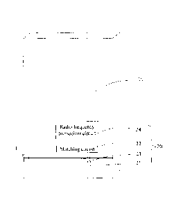
[0032] Referring to FIG. 2 and FIG. 2A, an exemplary implementation
manner of the
present invention provides an integrated structure of a metal housing and an
antenna of an
electronic apparatus, which includes an electronic apparatus 10. The
electronic apparatus 10
includes a metal housing (not shown in the figures) and an antenna structure
20. The
5
CA 02953629 2016-12-23
antenna structure 20 includes an antenna main body 21. At least one micro gap
set is
disposed on the metal housing. The at least one micro gap set includes micro
gaps. The
micro gap set divides the metal housing to form at least one metal region, and
the at least
one metal region is connected to the antenna main body 21 to serve as a
radiating body of
the antenna main body 21.
[0033] Specifically, the antenna structure 20 further includes a matching
circuit 22 and a
radio frequency transceiver circuit 24. The matching circuit 22 is located
between the radio
frequency transceiver circuit 24 and the antenna main body 21, and is
electrically connected
to the radio frequency transceiver circuit 24 and the antenna main body 21.
The matching
circuit 22 is used to adjust impedance matching of the loop antenna, so that
the antenna
main body 21 can better receive a radio frequency signal. The antenna main
body 21 and the
metal region may be connected by using a metal dome or connected by using a
screw. The
antenna main body is provided with a feed point 23, where the feed point 23 is
disposed on
the antenna main body 21. The micro gap may be formed by means of laser
cutting, and run
.. through the metal housing. A width of the micro gap is less than 0.5
millimeter, and in this
embodiment, preferably, the width is 0.03 millimeter. The micro gap set may
include several
micro gaps, and the several micro gaps are arranged and disposed at intervals
or are
crosswise disposed. Referring to FIG. 2A, a nonmetal material may fill between
every two
micro gaps. FIG. 9 is a diagram of antenna return loss generated by the
antenna main body
21 connected to the metal region.
[0034] According to the integrated structure of a metal housing and an
antenna of an
electronic apparatus in the present invention, a micro gap set including micro
gaps is
disposed on a metal housing to divide the metal housing into discontinuous
regions; the
micro gap set has an isolation effect on an antenna and the metal housing; and
the divided
.. metal housing is connected to an antenna main body 21 to serve as a
radiating body of the
antenna main body 21, thereby implementing an antenna function, which avoids
interference of the metal housing on an antenna signal and is beneficial to
barely see the
gap set from an appearance of the electronic apparatus, thereby not affecting
wholeness
and appearance beauty of an electronic apparatus 10 that uses the metal
housing.
6
CA 02953629 2016-12-23
[0035] Further, in a first embodiment of the present invention, there is
one micro gap
set, and the micro gap set divides the metal housing into two independent
metal regions.
Referring to FIG. 3, in this embodiment, the metal housing 25 is a back cover
of the
electronic apparatus 10, the micro gap set 30 includes more than three micro
gaps 31, and
the micro gap set 30 laterally runs through the metal housing 25 to divide the
metal housing
25 into independent metal regions 251 and 252. The antenna main body 21 is
connected to
the metal region 251. The metal region 251 serves as a radiating body of the
antenna main
body 21 to implement an antenna function. In another form of this manner, the
metal
housing 25 is a back cover connected to a metal peripheral frame, and the
micro gap set 30
extends to a position of the metal peripheral frame. The metal housing may
further be a
front housing of the electronic apparatus. It should be noted that, the micro
gap set 30 may
further longitudinally run through the metal housing 25.
[0036] Further, referring to FIG. 4, in a second embodiment of the
present invention,
there are two micro gap sets, and the micro gap sets divide the metal housing
to form two
metal regions that are completely separated. In this embodiment, the metal
housing 35 is a
peripheral frame of the electronic apparatus. The two micro gap sets 40
include more than
two micro gaps 41. The two micro gap sets 40 are disposed at intervals to
divide the
peripheral frame, so as to form the metal regions 351 and 352. The antenna
main body 21 is
connected to the metal region 351. The metal region 351 serves as a radiating
body of the
antenna main body 21 to implement an antenna function. Referring to FIG. 5, in
another
form of this implementation manner, the metal housing 35 is a peripheral frame
connected
to a metal back cover. The two micro gap sets 40 divide the metal housing 35
to form metal
regions 353 and 354. The antenna main body 21 is connected to either of the
metal regions,
which increases an area of the antenna main body 21, so as to improve
performance of the
antenna.
100371 Further, in a third embodiment of the present invention, there is
one micro gap
set, and the micro gap set partially divides the metal housing to form one
metal region.
Referring to FIG. 6, the metal housing 45 is a back cover of the electronic
apparatus. The
micro gap set 50 includes more than two micro gaps 51. The micro gap set 50 is
disposed at
7
CA 02953629 2016-12-23
a corner that is on the metal housing 45 and is close to the antenna main body
21, so that
the metal housing 45 becomes a metal region 451 partially partitioned by the
micro gap set
50. The antenna main body 21 is further provided with a ground point 26, and
the ground
point 26 is disposed on the metal region 451 on one side of the micro gap set
50. Referring
to FIG. 7, in another manner of this embodiment, the metal housing 45 is a
peripheral frame,
and the micro gap set 50 partitions the peripheral frame.
[0038] Referring to FIG. 8, a fourth exemplary implementation manner of
the present
invention provides an integrated structure of a metal housing and an antenna
of an
electronic apparatus, which includes an electronic apparatus 10. The
electronic apparatus 10
includes a metal housing 12, a circuit board 14, and an antenna structure 20.
The antenna
structure 20 includes an antenna main body 21. At least one micro gap set 60
is disposed on
the metal housing 12. The at least one micro gap set 60 includes micro gaps.
The micro gap
set 60 divides the metal housing 12 to form at least one metal region 121.
[0039] A difference between this implementation manner and the foregoing
three
implementation manners lies in that: the at least one metal region 121 is
connected to
ground of the circuit board 14 of the electronic apparatus 10, to serve as
reference ground
of the antenna main body 21. Implementation manners of the micro gap set 60
and the
metal housing 12 include the implementation manners in the foregoing three
embodiments,
and details are not described by using examples herein again. According to
this embodiment
of the present invention, the integrated structure of a metal housing and an
antenna of an
electronic apparatus is applied to a terminal, and because more electronic
elements are
mounted in the integrated structure of a metal housing and an antenna of an
electronic
apparatus, space of the terminal is saved. The following descriptions are
exemplary
implementation manners of the present invention. It should be noted that a
person of
ordinary skill in the art may make certain improvements and polishing without
departing
from the principle of the present invention and the improvements and polishing
shall fall
within the protection scope of the present invention.
8