Note: Descriptions are shown in the official language in which they were submitted.
- 1 -
Title
Plug connector and component
The invention relates to a plug connector and a component having an electrical
circuit ground.
The invention further relates to a use of the plug connector according to the
invention and the
component.
Prior art
The published patent application DE 197 27 092 Al describes a shielded
electrical plug
connector that contains shielded loops. The shielding loops are arranged in
several groups,
whereby there is a multitude of cable runs which can be connected to an
electrical circuit
ground of a circuit board. Because of the special arrangement, a low inductive
connection of
the shielding to the electrical circuit ground is obtained, whereby the
effectiveness of the
shielding at higher signal frequencies is optimised.
The published patent application DE 10 2008 006 340 Al describes a plug
connector having
a shaped shielding housing. A first stripped cable section is contacted by a
terminal element,
for example by means of crimping. The corresponding cable section is
additionally contacted
by an earth rail via a shielding. The earth rail is preferably formed from a
material with low
electrical impedance in order to enable controlling the earthing resistor for
the shielding. A
conductive plug connector seal element seals possible leakage current paths
for high
frequency disturbances and reduces the impedance of a connection between the
shielding
and the electrical circuit ground. In doing so, the connection between the
shielding and the
electrical circuit ground or the earth rail is implemented with as low a level
of impedance as
possible in order to ensure an effective shielding at high frequencies.
Date Recue/Date Received 2020-06-09
CA 02954564 2017-01-09
WO 2016/008473
PCT/DE2015/100275
- 2 -
The published patent application DE 42 22 452 Al describes a shielded plug
connector. The
relatively thin ground and shielding contacts inserted on their edges form a
connection which
bites into a conducting shielding and ground layer of the inserted plug
connector and thus
forms a stable electrical connection of the shielding and ground wire with as
low an impedance
as possible.
The utility model specification DE 93 12 470 U1 relates to a coaxial plug
connector. The known
plug connector provides the opportunity to automatically connect and
disconnect a terminal
resistor in an antenna socket, said terminal resistor then being looped in
between a neutral
conductor, i.e. a signal contact element, and an outer sleeve against the
electrical circuit
ground, if no complementary plug connector is inserted into the plug
connector. The value of
the terminal resistor should correspond to the surge impedance of the antenna
wire.
In the published patent application DE 101 19 695 Al, a plug connector is
described, in which
the two plug connection elements of the plug connector are provided in each
case with
shielding plates. The shielding plates substantially lie completely one on top
of the other in the
contacted state of the two plug connection elements, whereby a low inductive
and altogether
low ohmic shielding signal path is achieved.
In the published patent application US 6 976 886 B2, a plug connector is
described, in which
a high shielding effect of the signal guiding wire against one another and of
the plug connector
altogether is to be achieved by a special arrangement and alignment of the
signal guiding and
shielding or ground potential guiding contact elements relative to one
another. The known plug
connector is especially suitable for high frequency signals, wherein the
arrangement of the
signal guiding and ground potential guiding contact elements is furthermore
especially
predetermined for achieving a particular surge resistance.
In the published patent application DE 198 07 713 Al, a plug connector is
described that
contains a large number of contact elements. The known plug connector is
provided for
producing plug connections between backplanes and insertion cards, wherein, in
the practical
exemplary embodiment, plug connections between backplanes and insertion cards
or so-
called compact PCI systems are produced.
In the reference book by Meinke and Gundlach "Taschenbuch fur
Hochfrequenztechnik"
("Handbook for high frequency technology"), Springer-Verlag 1956, the basic
terms of
electrical technology such as capacitance, inductance and surge impedance are
explained.
- 3 -
The object of the invention is to specify a plug connector that enables a high
suppression of
disturbing signals by simple means.
Advantages of the invention
The invention firstly relates to a plug connector that has contact elements
that are divided into
at least one signal contact element and at least one shielding contact
element. The invention
further relates to a component that is to contact the plug connector or is
already contacting it,
said component providing an electrical circuit ground. The plug connector
according to the
invention and the component are characterised by an ohmic resistor which
connects a
shielding contact element of the plug connector to the electrical circuit
ground.
The plug connector according to the invention having the component is
particularly suitable
for connecting signal wire, via which high frequency signals, for example
digital differential
signals, broadcast, the data rate of which can be in the region of up to 20
gigabytes/second
for example. Correspondingly, the base frequency of the signal frequency can
be in the region
of up to 20 gigahertz.
The measure provided according to the invention, namely the electrical
connection of the at
least one shielding contact element of the plug connector to a circuit ground
via an ohmic
resistor instead of a direct electrical connection avoids parasitic
oscillations. Such parasitic
oscillations which disadvantageously influence the signal-broadcasting ratio
via the plug
connector and considerably worsen the signal quality, can arise when the
design height of the
plug connector that is directly soldered to the electrical circuit ground,
which provides the
component, is in the region of the half surge length of the parasitic
oscillations. The ohmic
resistor provided according to the invention and inserted between a shielding
contact element
and the electrical circuit ground obviously works as damping resistor and
prevents such
parasitic oscillations already emerging.
Date Recue/Date Received 2020-06-09
CA 02954564 2017-01-09
WO 2016/008473
PCT/DE2015/100275
- 4 -
A first embodiment provides that the resistance value of the ohmic resistor
corresponds to the
surge resistance of a signal wire guided via the plug connector (10). It has
been ascertained
in an experimental and calculated manner that an optimal suppression of
parasitic oscillations
is achieved by this calculation of the resistance value. According to one
embodiment, the
resistance value of the ohmic resistor can generally range from 20 ¨ 100 ohms,
wherein,
according to a special embodiment, the resistance value of the ohmic resistor
can be at least
approximately 50 ohms.
Another embodiment provides that such a ohmic resistor is precisely allocated
to a shielding
contact element in each case. An alternative embodiment to this that reduces
the required
number of ohmic resistors provides that an ohmic resistor is allocated to
several shielding
contact elements, wherein the shielding contact elements are in this case
directly electrically
connected to one another.
The at least one ohmic resistor can already be arranged directly in the plug
connector.
Alternatively, the at least one ohmic resistor can be allocated to the
component. Purely in
principle, a division of the ohmic resistor could also be provided in which
one part of the ohmic
resistor is arranged within the plug connector and one part of the ohmic
resistor on the
component. Purely in principle, a free wire of the ohmic resistor can be
provided in which the
ohmic resistor is arranged neither directly within the plug connector nor
directly on or in the
component.
A particularly advantageous embodiment provides that the plug connector is
surrounded by at
least one shielding, wherein the shielding is preferably directly connected to
the electrical
ground circuit. The shielding effectively prevents the emission of disturbing
signals from the
plug connector and correspondingly extensively suppresses the coupling of
external disturbing
signals in the plug connector. The at least one shielding contributes to
suppressing the
parasitic oscillations if they emerge.
One development provides that the component is a circuit board. In particular,
the circuit board
can be a backplane circuit board which is provided for receiving insertion
cards.
Another embodiment provides that the circuit board is a multi-layer circuit
board and a layer
of the multi-layer circuit board at least partially has an electrically
conductive surface with the
potential of the electrical circuit ground. A simple implementation of the
electrical ground circuit
- 5 -
becomes possible by this measure, wherein the flat design of the ground
circuit at the same
time provides a shielding effect.
One development provides that a plug connector corresponding to the plug
connector is
provided that has contact elements that are divided into at least one signal
contact element
and at least one shielding element. Furthermore, a second component having a
second
electrical ground circuit is provided. By doing so, a corresponding shielding
contact element
of the corresponding plug connector is connected to a second electrical ground
circuit via an
electrical resistor. It has become apparent that, by this measure, which is
provided on both
sides of the plug connector, a further improvement in the suppression of
parasitic oscillations
is achieved.
A further advantageous embodiment also contributes to this, said embodiment
providing that,
with plug connectors contacting one another, the electrical circuit ground
that is allocated to
the plug connector and a second electrical circuit ground that is allocated to
the corresponding
plug connector are directly electrically connected to each other. The
potential compensation
is preferably produced via contact elements within the two plug connectors.
A preferable usage of the plug connector and of the component or of the
corresponding plug
connector and of the second component is given by adjacent contact elements
forming a
signal contact element pair, wherein at least one shielding contact element is
allocated to the
signal contact element pair. This usage of the plug connector according to the
invention and
of the component is particularly suitable for connecting signal guiding wires
which guide
differential signals.
Further advantageous developments and embodiments of the plug connector
according to the
invention and of the component arise from the following description.
Short description of the exemplary embodiments
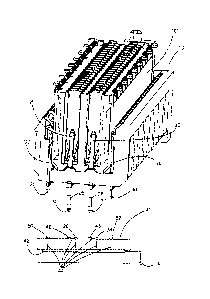
The exemplary embodiments are explained in more detail by the drawing.
Figure 1 schematically shows an aerial view of one layout of a plug connector,
Figure 2 shows the plug connector before contacting with a component and a
corresponding
plug connector in the plugged together state,
Date Recue/Date Received 2020-06-09
CA 02954564 2017-01-09
W02016/008473
PCT/DE2015/100275
- 6 -
Figure 3 shows the arrangement shown in Figure 2, in which the corresponding
plug connector
is depicted before contacting with a second component,
Figure 4 shows an alternative exemplary embodiment of the arrangement shown in
Figure 2
and
Figure 5 shows an alternative exemplary embodiment of the arrangement shown in
Figure 3.
Detailed description of the exemplary embodiments
Figure 1 schematically shows an aerial view of one layout of a plug connector
10 that has at
least two contact elements, preferably however a multitude of contact
elements. The contact
elements are divided up into at least one signal contact element and at least
one shielding
contact element. For example, a signal contact element 12 can be provided that
is arranged
to be adjacent to a shielding contact element 14.
In the depiction shown in Figure 1, a symbol, such as a plus sign for example,
should denote
a signal contact element 12 and a hatching should denote a shielding contact
element 14.
The shown signal contact element 12 and the adjacent shielding contact element
14 are
provided to connect a signal guiding wire that is not shown, wherein the
signal guiding wire
can have a signal wire connected to the signal contact element 12 and a
shielding wire
connected to the shielding contact element 14.
The plug connector 10 can preferably be used for connecting signal guiding
wires that contain
at least one pair of signal guiding wire that is connected to a signal contact
element pair 16
that comprises two directly adjacently arranged signal contact elements 18a,
18b. The signal
contact element pair 16 is preferably used for connecting differential signals
that are
characterised by a plus symbol and by a minus symbol in Figure 1. Such a
differential signal
has, in terms of a central level, for example a positive level on the one
signal contact element
(plus) and at the same time a negative level on the adjacent signal contact
element (minus) of
the signal contact element pair 16. The level changes in a push-pull manner
with the signal
frequency.
The signal guiding wire not shown that is connected to the signal contact
element pair 16
contains at least one shielding wire, wherein, in the shown exemplary
embodiment, two
shielding wires should be provided that are to be connected in each case to a
shielding contact
element 20, 22. The shielding contact elements 20, 22 are preferably arranged
directly
CA 02954564 2017-01-09
WO 2016/008473
PCT/DE2015/100275
- 7 -
adjacently with respect to the associated signal contact element pair 16 in
order to achieve
the best shielding effect.
It is provided according to the invention that at least one shielding contact
element 14, 20, 22
is not connected directly to a first electrical circuit ground 30, but rather
via an ohmic resistor
24, 26, 28. In the shown exemplary embodiment, along with the one shielding
contact element
14, the shielding contact elements 20, 22 allocated to the signal contact
element pair 16 are
also connected in each case via an ohmic resistor 26, 28 to the first
electrical circuit ground
30.
It should be noted that not every shielding contact element 14, 26, 28 of the
connector plug
10 has to be connected to the electrical circuit ground 30 via an ohmic
resistor, but can also
be connected directly to the first electrical circuit ground 30.
The first electrical circuit ground 30 is present in a first component not
shown in more detail in
Figure 1, the plug connector 10 either already being soldered to said
component or is to be
soldered as part of a mounting process.
The ohmic resistor 24, 26, 28 can be arranged within the plug connector 10.
Alternatively or
additionally, the ohmic resistor 24, 26, 28 can also be arranged on the first
component.
Preferably, high frequency signals, for example digital differential signals,
are broadcast via
the connector plug 10, the data rate of said signals being able to be in the
region of up to 20
gigabytes/second for example. K, corresponding to a base frequency of 20
gigahertz.
Based on experiments on practical plug connections that are supplied with very
high data
rates, it has been shown that, with direct contact of the shielding contact
element 14, 20, 22
by the first electrical circuit ground 30, parasitic oscillations can arise
which are in the
frequency region of 17 ¨ 18 gigahertz for example. Such a resonance point in a
plug
connection can disadvantageously influence the signal-broadcast ratio via the
plug connector
10.
The unwanted resonance can be guided back along the length of the signal path
in the plug
connector 10. The previously mentioned resonance frequency in the region of
around 17 ¨ 18
gigahertz corresponds to a surge length of around 10 millimetres on the
assumption that the
effective relative dielectricity constant amounts to around 2.8. The plastics
used for the plug
CA 02954564 2017-01-09
WO 2016/008473
PCT/DE2015/100275
- 8 -
connector 10 can have such a dielectricity constant. With an assumed design
height of the
plug connector 10 of 5 millimetres, the design height at least approximately
corresponds to
half the surge length and can therefore explain the emergence of the
resonance.
The parasitic oscillations do not only influence the signal-broadcast ratio
via the related signal
contact element 12, 18a, 18b, but also adjacent signal contact elements
because of the
electro-magnetic expansion inside the plug connector 10 and should therefore
also be avoided
for this reason.
It has been found in a calculated and experimental manner that the ohmic
resistor according
to the invention 24, 26, 28 that is inserted between the shielding contact
element 14, 20, 22
and the first electrical circuit ground 30 works as a damping resistor and
extensively gets rid
of the energy of the electrical oscillation at the resonance frequency that is
emerging, such
that the disturbing resonance frequency cannot form.
The resistance value of the ohmic resistor 24, 26, 28 is preferably in the
region between 20 ¨
100 ohms. According to a special exemplary embodiment, the resistance value of
the ohmic
resistor 24, 26, 28 can amount to at least approximately 50 ohms. In
particular, a resistance
value of the ohmic resistor 24, 26, 28 that corresponds to the surge
resistance of the signal
wire guided via the plug connector 10 is suitable. Details for determining the
capacitance
coating and the inductance coating of the plug connector 10 and the surge
resistance can be
found in the reference book by Meinke and Gundlach stated at the beginning, in
particular
pages 14, 18 and 165.
The plug connector 10 preferably has a shielding 32, 34 that is directly
connected to the first
electrical circuit ground 30. In the shown exemplary embodiment it is assumed,
for example,
that the plug connector 10 has such a shielding 32, 34 on both sides and both
shieldings 32,
34 are directly connected to the first electrical circuit ground 30.
Along with the plug connector shown in Figure 1, Figure 2 shows an exemplary
embodiment
of the first component 40 that is a plate, for example, with which the plug
connector 10 is
contacted during the mounting procedure. The first electrical circuit ground
30 is allocated to
the first component 40.
CA 02954564 2017-01-09
WO 2016/008473
PCT/DE2015/100275
- 9 -
The components shown in Figure 2 that are identical to the components shown in
Figure 1
are in each case provided with the same reference sign. This agreement also
applies to the
following Figures 3 ¨ 5.
According to Figure 2, as an exemplary embodiment of the first component 40,
the circuit
board can be implemented as a multi-layer circuit board, for example. In doing
so, the first
electrical circuit ground 30 can preferably be implemented as an electrically
conductive layer
42 on one of the layers of the multi-layer circuit board such that the first
electric circuit ground
30 has a shielding effect at the same time.
If the ohmic resistor 24, 26, 28 is to be arranged on the first component 40
outside the plug
connector 10, the ohmic resistor 24, 26, 28 is preferably positioned on the
uppermost layer of
the circuit board and is connected on one side to contact surfaces 46, 48 and
on the other
side to the first electrical circuit ground 30 via as short connection wires
44 as possible.
In the shown exemplary embodiment the two shieldings 32, 34 of the plug
connector 10 are
also to contact the contact surfaces 50, 52 or are already in contact with
them, wherein the
contact surfaces 50, 52 are also preferably connected to the first electrical
circuit ground 30
on the shortest possible path via the connection wires 44,
In the exemplary embodiment shown in Figure 2, a plug connector 10'
corresponding to the
plug connector 10 is shown, the former being depicted in the state of being
inserted into the
plug connector 10.
Figure 3 shows an exemplary embodiment according to which a second component
40',
preferably also a circuit board, can also be allocated to the corresponding
plug connector 10'.
The second component 40' can again be implemented as a multi-layer circuit
board. Figure 3
also shows here a state in which the corresponding plug connector 10' is not
yet in contact
with the second component 40', for example by means of soldering.
The corresponding plug connector 10' should contain at least one corresponding
contact
element 12' and one corresponding shielding contact element 14'. Preferably,
the
corresponding plug connector 10', however, contains a multitude of contact
elements,
including at least one corresponding signal contact pair 16' that contains
corresponding signal
contact elements 18a', 18b', said contact pair being positioned to be adjacent
to at least one
corresponding shielding contact element 20', 22'.
CA 02954564 2017-01-09
W02016/008473
PCT/DE2015/100275
- 10 -
Also, in the corresponding plug connector 10', the at least one corresponding
shielding contact
element 14', 20', 22' is not directly connected to a second electrical circuit
ground 30', but also
respectively via an ohmic resistor 26', 28'. In this case, the second
electrical circuit ground 30'
is allocated to the second component 40'.
It can also be provided in this exemplary embodiment that the ohmic resistor
26', 28' is
arranged inside the second plug connector 10'. Preferably however, the ohmic
resistor 26',
28' is provided on the second component 40' in this exemplary embodiment too.
In one implementation of the second component 40' as a multi-layer circuit
board, the second
electrical circuit ground 30' can again be formed on a separate layer of the
multi-layer plate
as a larger electrically conductive surface 42' in order to also achieve a
shielding effect in the
second component 40'.
lithe ohmic resistor 24, 26, 28 is to be arranged outside the corresponding
plug connector 10'
on the second component 40', the ohmic resistor 24', 26', 28' is preferably
again positioned
on the uppermost layer of the circuit board and connected on one side to
contact surfaces 46',
48' and on the other side to the second electrical circuit ground 30' by as
short connection
wires as possible.
According to the shown exemplary embodiment, the corresponding plug connector
10' can
also have corresponding shieldings 32', 34' that are to contact the contact
surfaces 50', 52'
on the second component 40' or are already in contact with them, wherein the
contact surfaces
50', 52' are also again preferably connected on the shortest possible path to
the second
electrical circuit ground 30' via connection wires 44'.
In the exemplary embodiment shown in Figure 3, in which at least one ohmic
resistor 26', 28'
or a second electrical circuit ground 30' is also allocated to the
corresponding plug connector
10', it is assumed that the first electrical circuit ground 30 of the first
component 40 has the
same potential as the second electrical circuit ground 30' on the second
component 40'. To
carry out the potential compensation it can be provided that at least one
contact element of
the plug connector 10 or of the corresponding plug connector 10' is provided
for directly
connecting the first electrical circuit ground 30 and the second electrical
circuit ground 30'.
Purely in principle, the potentials of the first and second electrical circuit
ground 30, 30' could
CA 02954564 2017-01-09
WO 2016/008473
PCT/DE2015/100275
- 11 -
deviate from each other, however, in practice, the circuit grounds 30, 30'
should be the same
as far as possible.
Figure 4 shows an embodiment that is an alternative to the exemplary
embodiment shown in
Figure 2, according to the former embodiment at least two shielding contact
elements 20a,
20b are directly electrically connected to each other by means of a connection
60, and wherein
the shielding contact elements 20a, 20b connected to each other are connected
to the first
electrical circuit ground 30 via a single ohmic resistor 62. The electrical
connection 60 can be
inside the plug connector 10. Alternatively, the connection 60 between the at
least two
shielding contact elements 20a, 20b can be provided on the first component 40
that is no
longer shown in Figure 4. Likewise, the ohmic resistor 62 can be arranged for
coupling the
connection 60 to the first electrical circuit ground 30, either still in the
plug connector 10,
preferably however on the first component 40.
Figure 5 shows an embodiment that is an alternative to the exemplary
embodiment shown in
Figure 3, according to which former embodiment at least two corresponding
shielding contact
elements 20', 22' are directly electrically connected to each other by means
of a connection
60' and wherein the directly corresponding shielding contact elements 20', 22'
that are
electrically connected to one another are connected to the second electrical
circuit ground 30'
.. via one single ohmic resistor 62'.
The electrical connection 60' can be inside the corresponding plug connector
10'. Alternatively,
the connection 60' between the at least two shielding contact elements 20',
22' can be
provided on the second component 40' no longer shown in Figure 4. Likewise,
the ohmic
resistor 62' can be arranged for coupling the connection 60' to the second
electrical circuit
ground 30' either still in the corresponding plug connector 10', preferably
however on the
second component 40'.