Note: Descriptions are shown in the official language in which they were submitted.
CA 2959680 2017-03-20
CONTROL DEVICE AND METHOD FOR MINIMIZING
SCALE FACTOR ERRORS OF A ROTATION RATE SENSOR
Field of the invention:
The invention is concerned with a device for minimizing a scale factor error
of a
rotation rate sensor caused by reference voltages and with a method for
minimizing the
scale factor error.
Background:
In many sensors of today's technology control circuits are used to control
single
elements of sensors and to adjust them to specific values. Here, it is often
necessary to
convert a digital control variable into an analog signal by which the element
to be
controlled can be driven directly. On the other hand, it may be necessary to
convert an
analog measurement signal, which describes the reaction of the element in
response to
the analog control signal, into a digital signal that can be compared to the
control
variable. To this end, digital-to-analog converters and/or analog-to-digital
converters
are used in sensors for converting the digital into analog and the analog into
digital
signals, respectively.
The digital-to-analog and the analog-to-digital converters use reference
voltages to
sample the digital and/or analog signals and to convert them. Typically, the
digital-to-
analog and/or analog-to-digital converters are integrated into the sensors as
prefabricated elements. Here, the problem occurs that the reference voltages
used by the
converters are not constant over time, but can take in the course of time
higher or lower
values due to aging. An inherent source for errors in the operation of the
sensors that
depend on digital-to-analog and/or analog-to-digital converters is therefore
aging of the
reference voltages used in these converters. The measurement precision of a
sensor is
affected directly by the aging of the reference voltages, if these are used as
scale factors
in calculating measurement values by the sensor.
Docket : 11253-038
CA 2959680 2017-03-20
2
It is therefore desirable to provide a device that minimizes a scale factor
error caused by
aging of reference voltages. Similarly, it is desirable to provide a method
for
minimizing such a scale factor error.
Particularly in, the field of rotation rate sensors nowadays digital-to-analog
converters
and analog-to-digital converters are used. Fig. 1 shows a schematic block
diagram of a
rotation rate sensor 100. The rotation rate sensor 100 comprises an excitation
mass 110
that is connected via first spring elements 120 to a substrate. The spring
elements 120
are formed such that the excitation mass 110 is able to oscillate with respect
to the
substrate in a first direction, whereas an oscillation in a second direction
perpendicular
to the first direction is prevented by the specific form of the first spring
element 120.
According to the example of the rotation rate sensor 100 illustrated in Fig. 1
the
excitation mass 110 is allowed to oscillate along the x-direction, whereas a
deflection
along the y-direction is prevented by the form of the first spring element
120, which
form is parallel to the y-direction.
Typically, in the rotation rate sensor 100 the oscillation of the excitation
mass 110 along
the x-direction is generated by excitation electrodes 130. The oscillation is
excited by
applying specific voltages to the excitation electrodes 130, which are
suitable for the
excitation. For example, applying an AC voltage to the excitation electrodes
130 leads
to a changing electrostatic attraction between the excitation electrodes 130
and
electrodes 132 that are connected to the excitation mass 110. This leads to
the
oscillation along the x-axis.
A readout mass 140 is connected via second spring elements 150 to the
excitation mass
110. The second spring elements 150 are formed such that the readout mass 140
is
allowed to oscillate along the second direction perpendicular to the first
direction,
whereas an oscillation of the readout mass 140 with respect to the excitation
mass 110
along the first direction is prevented by the form of the second spring
elements 150. In
the example illustrated in Fig. 1 the readout mass 140 may be deflected along
the y-
Docket : 11253-038
CA 2959680 2017-03-20
3
direction, but not along the x-direction. A deflection of the readout mass 140
is detected
via the change of a voltage applied to readout electrodes 160. The change in
voltage at
the readout electrodes 160 allows determining frequency and amplitude of the
oscillation of the readout mass 140.
The functional principle of a rotation rate sensor 100 designed according to
the block
diagram of FIG. 1 is to excite the excitation mass 110 along the x-direction
to a
precisely defined oscillation. If the rotation rate sensor 100 is rotated
around a direction
perpendicular to the x- and the y-direction, a Coriolis force will be
generated, which
deflects the readout mass 140 with respect to the excitation mass 110 along
the y-
direction. This deflection is proportional to the rotation rate. By means of
the readout
electrodes 160 that allow detecting the oscillations of the readout mass 140
it is, hence,
possible to determine the rotation rate of the rotation around the direction
perpendicular
to the x- and y-direction.
In order to be able to measure a wide range of rotation rates and in order to
obtain a
measurement behavior that is as linear as possible, the rotation rate sensor
100 is
typically read out such that a voltage is applied to the readout electrodes
that
counteracts an oscillation of the readout mass 140 with respect to the
excitation mass
110. If the size of the counteracting voltage is adjusted such that despite a
rotation no
oscillation of the readout mass 140 is excited, it is possible to determine
the rotation
rate by means of the applied voltage. The force compensating voltage may be
applied
for readout in time multiplex to the same readout electrode 160 or to separate
readout'
electrode(s) 160.
Hence, in a rotation rate sensor 100 according to the state of the art two
oscillations are
controlled by means of control loops. On the one hand, the oscillation of the
excitation
mass 110 along the x-direction is adjusted by means of the excitation
electrodes 130 to a
previously predetermined value. On the other hand, by means of the readout
electrodes
Docket : 11253-038
CA 2959680 2017-03-20
4
160 the oscillation of the readout mass 140 is suppressed, i.e. the amplitude
of the
oscillation is adjusted to the value zero.
To this end, typically two control loops are used that comprise each a digital-
to-analog
converter and an analog-to-digital converter. Each of these converters is
operated with a
reference voltage. The values of the reference voltages occur in a scale
factor that
defines the relation between the voltage that is necessarily applied to the
readout
electrodes and the rotation rate. The change of the reference voltage due to
aging has
therefore direct effects on the scale factor and hence on the measurement
precision of
the rotation rate sensor. In the worst case, i.e. if reference voltages age
such that aging
dependent errors cumulate, an error that is caused by the change of reference
voltages
affects the measurement result to the power of four.
Summary of invention:
The invention is concerned with the problem to provide a control device for
controlling
a rotation rate sensor, in which the scale factor error caused by changes,
i.e. aging, of
reference voltages can be minimized.
A control device for controlling a rotation rate sensor comprises a first
control loop and a second
control loop. The first control loop comprises a first control unit for
controlling an oscillation of
the rotation rate sensor along a first direction. In addition, the first
control loop comprises a first
digital-to-analog converter for converting a first digital control signal
output by the first control
unit into a first analog signal by means of which the oscillation of the
rotation rate sensor along
the first direction is controlled. Further, the first control loop comprises a
first analog-to-digital
converter for converting a first analog measurement signal that describes the
oscillation of the
rotation rate sensor along the first direction into a first digital readout
signal that is supplied to the
first control unit. The second control loop comprises a second control unit
for controlling an
oscillation of the rotation rate sensor along a second direction that is
different from the first
direction. In addition, the second control loop comprises a second digital-to-
analog converter for
converting a second digital control signal output by the second control unit
into a second analog
Docket: 11253-038
CA 2959680 2017-03-20
signal by means of which the oscillation of the rotation rate sensor along the
second direction is
controlled. Here, the first digital-to-analog converter, the second digital-to-
analog converter and
the first analog-to-digital converter operate during conversion each with a
reference voltage. In
addition, at least two of the reference voltages of the first digital-to-
analog converter, the second
5 digital-to-analog converter, and the first analog-to-digital converter
are dependent from each
other.
The aforementioned problem is also solved by a method for controlling a
rotation rate sensor. In a
first control loop the method comprises the steps of: converting with a first
digital-to-analog
o converter a first digital control signal output by a first control unit
for controlling an oscillation of
the rotation rate sensor along a first direction into a first analog signal by
means of which the
oscillation of the rotation rate sensor along the first direction can be
controlled, and converting
with a first analog-to-digital converter a first analog measurement signal
that describes the
oscillation of the rotation rate sensor along the first direction into a first
digital readout signal that
is supplied to the first control unit. In a second control loop the method
comprises the steps of:
converting with a second digital-to-analog converter a second digital control
signal output by a
second control unit for controlling an oscillation of the rotation rate sensor
along a second
direction perpendicular to the first direction into a second analog signal by
means of which the
oscillation of the rotation rate sensor along the second direction is
controlled. Here, the first
digital-to-analog converter, the second digital-to-analog converter and the
first analog-to-digital
converter operate each with a reference voltage during conversion. The method
comprises further
the step of: adjusting of a least two of the reference voltages of the first
digital-to-analog
converter, the second digital-to-analog converter, and the first analog-to-
digital converter such
that they arc dependent from each other.
This setup of a control device makes it possible to cancel during a change of
reference voltages of
the first digital-to-analog converter, the second digital-to-analog converter
and/or the first analog-
to-digital converter, e.g. due to aging, the detrimental effects of the change
because of
compensation due to the mutual dependency of at least two of the reference
voltages within the
Docket: 11253-038
CA 2959680 2017-03-20
6
scale factor. Due to this, the dependency of the scale factor e.g. from aging
of reference voltages
becomes less and a higher precision and reliability of the rotation rate
sensor can be achieved.
The dependency of the scale factor on changes of reference voltages, e.g. due
to aging,
can be reduced in this process from the fourth power to the second power. The
dependency of the scale factor on aging effects may even be totally cancelled.
It is also possible to use more than one first digital-to-analog converter,
one second
digital-to-analog converter or one first analog-to-digital, e.g. two first
digital-to-analog
converters, two second digital-to-analog converters, or two first analog-to-
digital
converters. The references voltages of these converters are then accordingly
dependent
from each other.
According to an advantageous example the reference voltage of the first analog-
to-
digital converter may be directly proportional to the reference voltage of the
first
digital-to-analog converter.
This ensures that a change of the reference voltage of the first analog-to-
digital
converter, e.g. because of aging, causes a change of the reference voltage of
the second
digital-to-analog converter in the same direction. This means that if the
reference
voltage of the first analog-to-digital converter becomes larger in the course
of time, also
the reference voltage of the second digital-to-analog converter will become
larger in the
course of time. On the other hand, for a reduction of the reference voltage of
the first
analog-to-digital converter also the reference voltage of the second digital-
to-analog
converter becomes smaller in the course of time. The rates of change of the
reference
voltages may have a constant ratio. This leads to a compensation of the
effects of the
changes within the scale factor of the rotation rate sensor and hence to an
enhanced
reliability and precision of the sensor. The scale factor depends then only to
the second
power on aging effects of reference voltages.
Docket: 11253-038
CA 2959680 2017-03-20
7
According to an advantageous example the reference voltage of the first analog-
to-
digital converter may be directly proportional to the reference voltage of the
first
digital-to-analog converter.
This ensures that during a change of the reference voltage of the first analog-
to-digital
converter, e.g. because of aging, the reference voltage of the first digital-
to-analog
converter changes in the same direction as the reference voltage of the first
analog-to-
digital converter. This means that if the reference voltage of the first
analog-to-digital
converter becomes larger in the course of time, also the reference voltage of
the first
digital-to-analog converter will become larger in the course of time. On the
other hand,
during a reduction of the reference voltage of the first analog-to-digital
converter also
the reference voltage of the first, digital-to-analog converter becomes
smaller in the
course of time. The rates of growth and/or reduction of the reference voltages
may be
coupled by a value that is constant in time, e.g. the rates of changes of the
reference
voltages may have constant ratios. This leads to a compensation of the effects
of
changes within the scale factor of the rotation rate sensor and hence to an
enhanced
reliability and precision of the sensor. The scale factor depends then only to
the second
power on changes or aging effects of the reference voltages.
According to an advantageous example the reference voltage of the first
digital-to-
analog converter may be directly proportional to the reference voltage of the
second
digital-to-analog converter and the reference voltage of the first analog-to-
digital
converter may simultaneously be directly proportional to the third power of
the
reference voltage of the first digital-to-analog converter.
This ensures that during a change of the reference voltage of the first
digital-to-analog
converter, e.g. because of aging, the reference voltage of the second digital-
to-analog
converter changes in the same direction as the reference voltage of the first
digital-to-
analog converter. This means that if the reference voltage of the first
digital-to-analog
converter becomes larger in the course of time, also the reference voltage of
the second
Docket : 11253-038
CA 2959680 2017-03-20
8
digital-to-analog converter will become larger in the course of time. On the
other hand,
during a reduction of the reference voltage of the first digital-to-analog
converter also
the reference voltage of the second digital-to-analog converter becomes
smaller in the
course of time. The rates of growth and/or reduction of reference voltages may
be
coupled over a value that is constant in time.
Simultaneously it is ensured that during a change of the reference voltage of
the fist
analog-to-digital converter, e.g. because of aging, the reference voltage of
the first
digital-to-analog converter changes in the same direction and to the third
power of the
reference voltage of the first digital-to-analog converter. This means that a
change of
the reference voltage of the first analog-to-digital converter by an amount A
changes ¨
for small A ¨ the reference voltage of the first digital-to-analog converter
by an amount
of 3A.
This leads to a compensation of changes or aging effects within the scale
factor of the
rotation rate sensor and hence to an enhanced reliability and precision of the
sensor. The
scale factor depends then only to the second power on changes or aging effects
of the
reference voltages. The dependency of the scale factor on changes or aging
effects of
the reference voltages may even by totally eliminated.
According to an advantageous example the reference voltage of the first
digital-to-
analog converter may be inversely proportional to the reference voltage of the
second
digital-to-analog converter or may change during aging in the opposite
direction than
the reference voltage of the second digital-to-analog converter.
This ensures that during a change of the reference voltage of the first
digital-to-analog
converter, e.g. because of aging, the reference voltage of the second digital-
to-analog
converter is changed in the opposite direction of the change of the reference
voltage of
the first digital-to-analog converter. This means that if the reference
voltage of the first
digital-to-analog converter becomes larger in the course of time, the
reference voltage
Docket : 11253-038
CA 2959680 2017-03-20
9
of the second digital-to-analog converter will become smaller in the course of
time. On
the other, during a reduction of the reference voltage of the first digital-to-
analog
converter the reference voltage of the second digital-to-analog converter
becomes larger
in the course of time. The rates of growth or reduction of the reference
voltages may be
coupled by a value that is constant in time, i.e. the rates of changes of the
reference
voltages may have constant ratios. This leads to a compensation of the changes
or aging
effects within the scale factor of the rotation rate sensor and hence to an
enhanced
reliability and precision of the sensor. The scale factor depends then only to
the second
power on changes or aging effects of the reference voltages.
According to an advantageous example the second control loop of the control
device
comprises a second analog-to-digital converter for converting a second analog
measurement signal that describes the oscillation of the rotation rate sensor
along the
second direction into a second digital readout signal that is supplied to the
second
control unit. This ensures that the readout electrode can be set to the
desired amplitude
correctly by converting and supplying the second analog measurement signal by
the
second control loop. This allows a full-fledged operation of the rotation rate
sensor
during which also effects due to changes of reference voltages caused by aging
on the
measurement results are reduced.
According to an advantageous example a rotation of the rotation rate sensor
around a
normal being perpendicular to the first direction and the second direction may
excite the
oscillation of the rotation rate sensor along the second direction. This
ensures that the
rotation rate sensor is suitable for measuring the rotation rate via the
Coriolis force,
which allows an operation of the rotation rate sensor by means of Coriolis
force
measurements in which changes or aging effects of reference voltages on the
measurement result are minimized.
Docket: 11253-038
CA 2959680 2017-03-20
According to an advantageous example the rotation rate sensor is a
microelectromechanical (MEMS) gyroscope. Then, the effects detailed above can
also
be used for the operation of rnicroelectromechanical gyroscopes.
.5 Brief description of the drawings:
In the following embodiments of the invention their functioning and their
advantages
will be describe with respect to the Figures. Elements of the embodiments can
be
combined with each other, if they do not exclude each other. It shows:
10 Fig. 1 a schematic block diagram of a rotation rate sensor
according to the prior
art.
Fig. 2 a schematic block diagram of a control device for controlling a
rotation
rate sensor according to an embodiment.
Fig. 3 a schematic block diagram of a control device for controlling a
rotation
rate sensor according to another embodiment.
Fig. 4 a schematic bock diagram of a control device for controlling a
rotation rate
sensor according to another embodiment.
Fig. 5 a control device for controlling a rotation rate sensor
according to another
embodiment.
Fig. 6 a schematic block diagram of a control device for controlling a
rotation
rate sensor according to another embodiment.
Fig. 7 a schematic process flow of a method for controlling a rotation
rate sensor
according to an embodiment.
Docket: 11253-038
CA 2959680 2017-03-20
11
Preferred embodiments of the invention:
In the Figures elements or groups of elements corresponding to each other are
denoted
with the same reference sign.
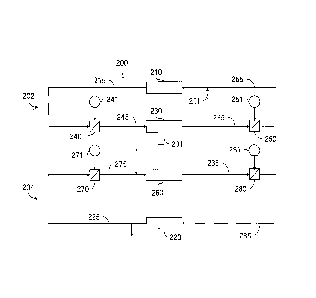
Fig. 2 shows a schematic block diagram of a control device 200 for controlling
a
rotation rate sensor. The rotation rate sensor may be a sensor as described
with respect
to Fig. I. The rotation rate sensor may for example be a micro-electro-
mechanical
sensor (MEMS).
The control device 200 comprises a first control loop 202 and a second control
loop 204.
The first control loop 202 comprises a first control unit 210 for controlling
an excitation
unit 230. The first control unit 210 may e.g. via the excitation unit 230
control an
oscillation of an MEMS or of the rotation rate sensor according to Fig. 1
along a first
direction, e.g. along the x-direction of Fig. I. To this end, the excitation
unit 230 may
comprise one or several excitation electrodes 130 and electrodes 132 as
illustrated in
Fig. 1.
The first control unit 210 outputs a first digital control signal 215 that is
converted by a
first digital-to-analog converter 240 in a first analog signal 245. The first
analog signal
245 is transferred to the excitation unit 230 and serves to adjust a frequency
and/or
amplitude of an oscillation that is excited by the excitation unit 230. The
excitation unit
230 outputs, if the corresponding excitation electrodes 130 are used in time
multiplex
also as readout electrodes, a first analog measurement signal 235 that
describes the
oscillation of the rotation rate sensor along the first direction. This signal
may also be
obtained via separate electrode pairs comprised in the excitation unit 230.
The first
analog measurement signal 235 is converted in a first analog-to-digital
converter 250 in
a first digital readout signal 255 that is compared to a controller signal 211
and supplied
to the first control unit 210.
Docket : 11253-038
CA 2959680 2017-03-20
12
The second control loop 204 comprises a second control unit 220 for
controlling a readout
unit 260 and hence for controlling an oscillation of the rotation rate sensor
along a
second direction that is different from the first direction. For example, the
read out 260
may comprise a readout electrode 160 according to Fig. 1 that detects an
oscillation of a
readout mass along the second direction that may be for example the y-
direction
illustrated in Fig. 1. The oscillation detected by the readout unit 260 is
caused by a
rotation of the rotation rate sensor, if the amplitude of the oscillation
controlled by the
first control loop 202 is different from zero. This is illustrated
schematically in Fig. 2 by
the Coriolis signal 231.
In first iteration the Coriolis signal 231 is measured by the readout unit 260
and
transmitted as second analog measurement signal 265 to a second analog-to-
digital
converter 280 where it is converted to a second digital readout signal 285.
The second
digital readout signal 285 is supplied to the second control unit 220 that
outputs a second
digital control signal 225 in order to set the oscillation of the rotation
rate sensor along
the second direction by means of electrodes that may be comprised in the
readout unit
260 to zero. The second digital control signal 225 is also output to the
exterior and
indicates the strength of the rotation of the rotation rate sensor.
In order to be able to control the readout unit 260 effectively the second
digital control
signal 225 is converted in a second digital-to-analog converter 270 in a
second analog
signal 275 that is supplied to the readout unit 260. By using the Coriolis
signal 231 and
the second analog signal 275 the amplitude of an oscillation of the rotation
rate sensor
along the second direction may be set to zero.
The first digital-to-analog converter 240 is operated with a reference voltage
URerol 241.
The first digital-to-analog converter 250 is operated with a reference voltage
URefA I 251
and the second digital-to-analog converter 270 is operated with a reference
voltage
URefD2 271. The reference voltages URcfm 241, URcfm 251, and URefD2 271
contribute to
the scale factor that brings the read out second digital control signal 225
into relation
Docket: 11253-038
CA 2959680 2017-03-20
13
with the rotation rate applied to the rotation rate sensor. In addition, the
second analog-
to-digital converter 280 may be operated with a reference voltage URcfA2 281.
By the analog-to-digital/digital-to-analog converters the reference voltages
are used to
determine an incoming signal by comparing it with the reference voltages and
are hence
used to determine its size.
According to an embodiment at least two of the reference voltages URcroi 241,
URcfAl
251, and URctD2 271 dependent from each other. This ensures that aging effects
of the
reference voltages URefDI 241, URefAl 251, and tiRcm2 271 compensate in the
scale factor
of the rotation rate sensor and hence that scale factor errors that are caused
by aging
effects are minimized. Therefore, use of the control device 200 enhances the
precision
and reliability of the rotation rate sensor operated with the control device
200.
Fig. 3 shows a schematic block diagram of a control device 300 for controlling
a
rotation rate sensor. The structure of the control device 300 corresponds
substantially to
the structure of the control device 200 shown in Fig. 2. Therefore, regarding
the
particular structure of the control device 300 reference is made to the
description of the
control device 200 illustrated in Fig. 2. Further, it should be noted that in
Fig. 3, and
also in Figs. 4, 5, and 6 described below, the reference voltage URefA2 281 of
the second
analog-to-digital converter 280 is not illustrated as this is not necessary
for the further
discussion of the embodiments of the control devices according to the present
invention.
The control device 300 differs from the control device 200 in that the
reference voltages
URefAl and URefD2 of the first analog-to-digital converter 250 and the second
digital-to-
analog converter 270 are directly proportional to each other. This is
illustrated in Fig. 3
by the common voltage source 352 from which the reference voltages of the
first
analog-to-digital converter 250 and the second digital-to-analog converter 270
are
derived.
Docket: 11253-038
CA 2959680 2017-03-20
14
This ensures that during a change of the reference voltage URefAi of the first
analog-to-
digital converter 250 the reference voltage URem2 of the second digital-to-
analog
converter 270 changes in the same direction as the reference voltage URcfAl=
This may
for example be achieved by the common voltage source 352 illustrated in Fig. 3
from
which the reference voltages thcfAl and URctD2 are derived. The reference
voltages
URciAi and URerp2 may correspond directly to the voltage of the common voltage
source
352, however, they may also be generated by scaling the voltage of the common
voltage
source 352. Then, the ratio of the reference voltages URefAl and thefD2 has a
value that is
constant in time.
Alternatively, it is also possible to determine via measurements of the
reference
voltages over a predetermined time period, e.g. at the manufacturer, whether a
reference
voltage of the digital-to-analog converter or an analog-to-digital converter
element that
is to be used without modification in the control device 300 gets larger or
smaller over
time. Then, as first analog-to-digital converter 250 and second digital-to-
analog
converter 270 such elements can be used whose reference voltage change in the
same
direction. This has the advantage that an existing circuitry does not need to
be changed,
but only elements must be chosen, whose aging characteristic is the same.
The control device 300 illustrated in Fig. 3 allows to reduce the dependency
of the scale
factor from the aging of the reference voltage to the second power.
Fig. 4 shows a control device 400 for controlling a rotation rate sensor
according to a
further embodiment. The control device 400 has substantially the same
structure as the
control device 200 of Fig. 2. Therefore, a detailed description of the
structure of the
control device 400 is omitted and it is referred to the description of the
control device
200.
The control device 400 differs from the control device 200 in that the
reference voltage
URcfAl of the first analog-to-digital converter 250 is directly proportional
to the
Docket: 11253-038
CA 2959680 2017-03-20
reference voltage URcIDI of the first digital-to-analog converter 240. This is
illustrated in
Fig. 4 by common voltage source 452 from which the reference voltages URcfAl
and
URet-DI of the first analog-to-digital converter 250 and the first digital-to-
analog
converter 240 derive, respectively.
5
This ensures that during a change of the reference voltage thefAl of the first
analog-to-
digital converter 250 the reference voltage URemi of the first digital-to-
analog converter
240 is changed in the same direction as the reference voltage URcfAl= This may
for
example be achieved by the common voltage source 452 that is illustrated in
Fig. 4,
10 from which the reference voltages URcfAl and URODI arc derived. The
reference voltages
thefAl and URcM1 may correspond directly to the voltage of the common voltage
source
452, however, they may also be generated by scaling of the voltage of the
common
voltage source 452. Then, the ratio of the reference voltages URefAl and
UlterD1 has a
value that is constant in time.
Alternatively, it is possible to determine via measurements of the reference
voltages
over a predetermined time period, e.g. at the manufacturer, whether a
reference voltage
of a digital-to-analog converter or analog-to-digital converter element that
is to be used
without modifications in the control device 400 becomes larger or smaller over
time.
Then, as first analog-to-digital converter 250 and as first digital-to-analog
converter 240
elements can be used whose reference voltages change in the same direction.
This has
the advantage that it is not necessary to change an existing circuitry, hut
only to choose
elements whose aging characteristic are the same.
By means of the control device 400 illustrated in Fig. 4 the dependency of the
scale
factor on the aging of reference voltages can be reduced to the second power.
Fig. 5 shows a schematic block diagram of a control device 500 for controlling
a
rotation rate sensor according to a further embodiment. The structure of the
control
device 500 corresponds substantially to the structure of the control device
200
Docket: 11253-038
CA 2959680 2017-03-20
16
illustrated in Fig. 2. Hence, here a detailed description of the control
device 500 is
omitted and it is referred to the description of the control device 200.
The control device 500 differs from the control device 200 in that the
reference voltage
URefDI of the first digital-to-analog converter 240 is inversely proportional
(i.e.
reciprocal) to the reference voltage URcfD2 of the second digital-to-analog
converter 270.
This is illustrated in Fig. 5 by the reciprocity element 542.
This ensures that during a change of the reference voltage URefDI of the first
digital-to-
analog converter 240 the reference voltage URefD2 of the second digital-to-
analog
converter 270 changes oppositely to the reference voltage URemi. This may for
example
be achieved by the reciprocity element 542 illustrated in Fig. 5 that either
outputs a
value reciprocal to the reference voltage URemi of the first digital-to-analog
converter
240 (i.e. it inverts the reference voltage URemi) and transfers it as
reference voltage
URefD2 to the second digital-to-analog converter 270, or that outputs a value
reciprocal to
the reference voltage URcM2 of the second digital-to-analog converter 270 and
transmits
it as reference voltage URenoi to the first digital-to-analog converter 240.
In addition, the
reference voltages URemi and URcfD2 may be scaled before and/or after
inverting. The
product of the reference voltages URcroi and URcID2 has then a constant value
in time.
Alternatively, it is possible to determine by means of measurements of the
reference
voltages over a predetermined time period, e.g. at the manufacturer, whether a
reference
voltage of one of the digital-to-analog converter elements that is to be used
without
modifications in the control device 500 is getting smaller or lager over time.
Then, as
first digital-to-analog converter 240 and as second digital-to-analog
converter 270 such
elements can be used whose reference voltages change oppositely from each
other. This
has the advantage that it is not necessary to change an existing circuitry,
but only to
choose elements whose aging characteristic is opposite.
By means of the control device 500 illustrated in Fig. 5 the dependency of the
scale
factor from aging of reference voltages can be reduced to the second power.
Docket: 11253-038
CA 2959680 2017-03-20
17
Fig. 6 shows a schematic block diagram of a control device 600 for controlling
a
rotation rate sensor according to a further embodiment. The structure of the
control
device 600 corresponds substantially to the structure of the control device
200.
Therefore, a detailed description of the control device 600 is omitted and it
is referred to
the description of the control device 200.
The control device 600 differs from the control device 200 in that the
reference voltage
URemi of the first digital-to-analog converter 240 is directly proportional to
the
reference voltage therD2 of the second digital-to-analog converter and that
the reference
voltage URefAi of the first analog-to-digital converter 250 is directly
proportional to the
third power of the reference voltage URcf-Di of the first digital-to-analog
converter 240.
This is illustrated in Fig. 6 by a common voltage source 652 and a raising
element 657.
This ensures that during a change of the reference voltage URcIDI of the first
digital-to-
analog converter 240 the reference voltage limp2 of the second digital-to-
analog
converter 270 changes in the same direction as the reference voltage URefDl=
This may
for example be achieved by the common voltage source 652 illustrated in Fig. 6
from
which the reference voltages thcfni and thcfn2 are derived. The reference
voltages
UltefD1 and them2 may correspond directly to the voltage of the common voltage
source
652, however, they may also be generated by scaling the voltage of the common
voltage
source 652. Then, the ratio of the reference voltages URcIDI and URcfD2 is
constant in
time.
Alternatively, it is possible to determined by measurements of the reference
voltages
over a certain time period, e.g. at the manufacturer, whether a reference
voltage of one
of the digital-to-analog converter elements that is to be used without
modifications in
the control device 600 becomes lager or smaller over time. Then, as first
digital-to-
analog converter 240 and as second digital-to-analog converter 270 such
elements can
be used whose reference voltages change in the same manner. This has the
advantage
Docket : 11253-038
CA 2959680 2017-03-20
18
that it is not necessary to change an existing circuitry, but only to choose
elements
whose aging characteristic is the same.
Simultaneously it is ensured that during a change of the reference voltage
URcfAl of the
first analog-to-digital converter 250 by an amount of A, with A being small,
the
reference voltage URefDI of the first digital-to-analog converter 240 is
changed by an
amount proportional to 3A. This may be achieved by connecting the inputs of
the raising
element 657 with the common voltage source 652, if the ratio of URefDI to
URefD2 is
constant over time. Alternatively, the input of the raising element 657 is
connected to
one of the reference voltages URefDl, URefD2 which change in the same manner,
as has
been determined based on measurements.
By means of the control device 600 illustrated in Fig. 6 the dependency of the
scale
factor on the aging of the reference voltages may be reduced to the second
power or may
even be totally eliminated.
According to further not illustrated embodiments the control devices
illustrated in Figs.
2 to 6 may be combined with each other in order to reduce the dependency of
the scale
factor from aging of reference voltages even further, if the illustrated
embodiments do
not exclude each other.
Fig. 7 shows a schematic process flow of a method for controlling a rotation
rate sensor
according to an embodiment.
At S700 in a first control loop a first control signal is converted into a
first analog signal
by means of a first digital-to-analog converter that uses a reference voltage.
At S710 in the first control loop a first analog measurement signal is
converted into a
first digital readout signal by means of a first analog-to-digital converter
that uses a
reference voltage.
Docket: 11253-038
CA 2959680 2017-03-20
19
At S720 a second digital control signal is converted in a second control loop
into a
second analog signal by means of a second digital-to-analog converter that
uses a
reference voltage.
At S730 at least two of the reference voltages of the first digital-to-analog
converter, the
second digital-to-analog converter and the first analog-to-digital converter
are adjusted
such that they depend from each other.
This ensures that aging effects of the reference voltages that contribute to
the scale
factor of the rotation rate sensor compensate such that scale factor errors
are minimized.
This makes the rotation rate sensor more precise and reliable.
According to further embodiments the reference voltages of the first digital-
to-analog
converter, the second digital-to-analog converter, and the first analog-to-
digital
converter can be adjusted according to one of the embodiments of a control
device
discussed above with respect to Figs. 3 to 6. Due to this, the dependency of
the scale
factor from aging effects of reference voltages can be reduced to a quadratic
dependency
or may be eliminated totally.
Docket: 11253-038