Note: Descriptions are shown in the official language in which they were submitted.
CA 02956317 2017-01-25
WO 2016/014935
PCT/US2015/041974
HYBRID LASER ANTI-CLIPPING FOR
FIBER-COAXIAL NETWORKS
BACKGROUND
[0001] Hybrid fiber-coaxial (HFC) networks include both fiber optic and
coaxial
connections and are commonly used to provide broadband data and video
services.
For example, HFC networks offer broadcast video, interactive television,
digital
video, high-speed data and Internet access, and telephony services. In a
typical
implementation, HFC networks deliver such broadband data services as optical
signals transmitted from head-end locations via an optical fiber to an optical
distribution node. On the downlink side (i.e., head-end location-to-subscriber
direction), the optical distribution node converts the optical signals to
radio frequency
(RF) signals and transmits the RF signals to subscriber locations via coaxial
cable
links. Some HFC networks allow for two-way communication. Such two-way HFC
networks usually include an uplink (i.e., subscriber-to-head-end location
direction)
communication connection, through which subscriber premises devices transmit
RF
signals to the optical distribution node that then converts the RF signals to
optical
signals for transmission back to the head-end location.
[0002] The RF signals in an HFC network are typically transmitted in the 5 MHz
to
1.8 GHz range. In some implementations, the frequency spectrum from 85 MHz to
1
GHz is used by the optical distribution node for downlink signals, while the
frequency
spectrum from 5 to 85 MHz is used by the subscriber premises devices for
uplink
signals. However, the actual split of the spectral band can vary by the
standard used.
Using such configurations, an HFC network can provide adequate two-way
services
for interactive services, such as Internet access, e-mail, voice/telephone
services, or
video on demand. However, the two-way services provided by existing HFC
networks are often limited by the bandwidth asymmetry in the downlink and
uplink
frequency spectra. As new two-way applications and services become more
popular,
the demand for HFC networks to provide symmetric high-quality high-bandwidth
1
CA 02956317 2017-01-25
WO 2016/014935
PCT/US2015/041974
services also increases. Interactive video, interactive gaming, video
telephony,
videoconferencing, remote storage, virtual DVD, and high-speed virtual private
networks (VPNs) are just a few such applications for existing two-way HFC
networks
may be inadequate. Increases in uplink, or so-called "return path," traffic
have
exposed limitations in the current HFC networks. In some implementations, the
optical link devices required to convert the RF uplink signals to optical
signals are the
limiting factor.
[0003] In many HFC networks, the return path signal is converted from the
electrical domain to the optical domain in the optical distribution node using
a directly
modulated semiconductor laser, such as diode laser. The simplicity of such
implementations comes at the cost of very stringent noise and distortion
requirements
on the laser. More complex, and consequently more expensive, distributed
feedback
(DFB) lasers have been proven to meet the voice and distortion requirements.
While
the additional cost associated with DFB lasers can sometimes be justified in
implementations in which extremely large populations of end users are served,
such
lasers still have limitations. While the channel capacity of DFB lasers is
large, such
devices are still inherently limited by the physical characteristics of the
semiconductor
laser. If the product of the number of channels and modulation depth per
channel
exceeds the threshold current of the laser, the modulation current will drop
below the
laser threshold current and shut off the laser. For example, if the RF input
signal
power to the laser goes beyond an inherent or characteristic limit, then
signal
distortion increases rapidly. Also, if RF input signal power goes
substantially above
that limit, distortion known as "laser clipping" occurs.
[0004] Laser clipping occurs when the modulating RF input signal current that
drives the semiconductor laser, in either the uplink or downlink directions,
occasionally falls below the laser's threshold current resulting in nearly
zero optical
power output. This behavior degrades the Bit Error Rate (BER) performance of
the
transmitted digital signal.
2
CA 02956317 2017-01-25
WO 2016/014935
PCT/US2015/041974
BRIEF DESCRIPTION OF THE DRAWINGS
[0005] FIG. 1 is a schematic diagram of a two-way hybrid fiber-coaxial (HFC)
network, according to embodiments of the present disclosure.
[0006] FIG. 2 is an illustrative characteristic noise-power-ratio (NPR) graph
for a
semiconductor laser module.
[0007] FIG. 3 is a schematic diagram of a HFC network with hybrid anti-
clipping
modules, according to embodiments of the present disclosure.
[0008] FIG. 4A is a schematic diagram of a hybrid anti-clipping module,
according
to embodiments of the present disclosure.
[0009] FIG. 4B is a schematic diagram of a conditioning circuit of a hybrid
anti-
clipping module, according to embodiments of the present disclosure.
[0010] FIG. 5 illustrates an RF input signal power profile with characteristic
average power and power envelope peaks.
[0011] FIG. 6 illustrates RF input signal power profiles and the resulting
modes of
operation of a hybrid anti-clipping module, according to embodiments of the
present
disclosure.
DETAILED DESCRIPTION
[0012] Described herein are techniques for systems, methods, and devices for
improving the RF input power dynamic range of optical transmitters in hybrid
fiber-
coaxial (HFC) networks using configurable hybrid anti-clipping circuits with
automatic RF gain and laser bias current controls. In the following
description, for
purposes of explanation, numerous examples and specific details are set forth
in order
to provide a thorough understanding of particular embodiments.
Particular
embodiments as defined by the claims may include some or all of the features
in these
examples alone or in combination with other features described below, and may
further include modifications and equivalents of the features and concepts
described
herein.
3
CA 02956317 2017-01-25
WO 2016/014935
PCT/US2015/041974
[0013] Hybrid Fiber-Coaxial Networks
[0014] FIG. 1 is a schematic diagram of an example two-way HFC network 100. As
shown, the HFC network 100 includes a number of user premises devices 105,
(e.g.,
cable modems and set-top-boxes), an optical distribution node 110, and a head-
end
server computer 140. The user premises devices 105 and the head-end server
computer 140 can exchange signals through corresponding hybrid RF-optical
paths in
the optical distribution node 110. In such embodiments, the terms "downstream"
and
"downlink" refer to the RF-optical path 120 through which data signals are
transmitted from the head-end server computer 140 to the user premises devices
105.
Similarly, the terms "upstream" and "uplink" refer to the RF-optical paths 130
through which data signals are transmitted from the user premises devices 105
to the
head-end server computer 140. Such
systems are often limited by various
electrical/optical characteristics, and in particular the laser clipping
characteristics, of
the optical link devices in the optical distribution node 110 and the head-end
server
computer that convert RF electrical signals to optical signals.
Accordingly,
improvements provided by various embodiments of anti-clipping systems,
methods,
and circuits described herein can be implemented in and realized by either the
downlink path 120 or the uplink path130.
[0015] The basic functionality of example HFC network 100 is described in
reference to FIG. 100 to provide context as to how various aspects of the
present
disclosure can improve overall system performance. In various embodiments, the
head-end server computer 140 receives data signals from data sources 150
(e.g.,
satellite feeds from television stations, data from websites on the Internet,
music from
online services, etc.). The data signals can include any type of information,
such as
video data, voice data, music data, and the like. The head-end computer system
140
can process and/or transcode the data signals before generating and
transmitting
corresponding optical data signals over one or more fiber optic connections
115 to
optical distribution node 110. When the optical signals are received by the
optical
distribution node 110, the signals can be converted from the optical domain
(e.g.,
optical frequencies and protocols) to the electrical domain (e.g., RF signals
and
protocols) in the downstream optical/RF path 120. In some embodiments, the
4
CA 02956317 2017-01-25
WO 2016/014935
PCT/US2015/041974
downstream optical/RF path 120 can include routing functionality for routing
the
resulting RF signals to one or more user premises devices 105 over
corresponding
electrical connections 107 (e.g., coaxial cables). In two-way communication
capable
HFC network 100, the user premises devices 105 can generate RF signals (e.g.,
requests for data or voice data) and transmit them to the optical distribution
node 110.
In the upstream RF/optical path 130, the RF signals are converted from the
electrical
domain to the optical domain. Conversion of the signals from the electrical
domain to
the optical domain includes the use of optical transmitter (e.g., a
semiconductor laser
module) that can be driven by the electrical signals to generate corresponding
optical
signals (e.g., modulated signals of light).
[0016] The inherent limitations of the optical transmitter used in optical
link to
convert signals from the electrical domain to the optical domain in the uplink
path 130
and downlink path 120 can impose significant limitations on the performance of
the
HFC network 100, both in terms of noise and distortion. The noise and
distortion in
the optical signal generated by a particular laser module often depends on the
density
of signals transmitted at a particular moment in time. For example, the noise
and
distortion of the optical signal in the upstream RF/optical path 130 through a
particular optical distribution node 110 depends on the number of subscriber
stations
(e.g., user premises devices 105) simultaneously transmitting an uplink
signal. In
other words, when the composite power of the RF input signals used to drive
the laser
module generating the corresponding optical signals exceeds a threshold level,
the
optical output signal become clipped, thus diminishing the fidelity and
bandwidth of
the optical signal. Accordingly, to control the noise and distortion it is
necessary to
understand the capabilities and characteristics of the laser module. Thus, in
addition
to BER measurements described above, it is useful to have another concise
metric to
describe the capabilities of the laser module. One such metric is the noise
power ratio
measurement.
[0017] Noise Power Ratio
[0018] Noise-power-ratio (NPR) measurements are commonly used to characterize
laser modules. Accordingly, the NPR measurement can be a valuable tool for
CA 02956317 2017-01-25
WO 2016/014935
PCT/US2015/041974
characterizing optical link performance and capability of laser modules for
use in anti-
clipping embodiments of the present disclosure. NPR curves provide a quick
picture
of an optical link's noise and distortion performance with one easy to
understand
performance curve.
[0019] NPR measurements include a test method that examines the amount of
noise
and intermodulation distortion. A test signal, usually including a flat
Gaussian noise
band limited to the frequency range of interest and within a narrow band
(e.g., a
channel), is injected into the laser module. The NPR is measured at the output
of the
laser module as the test signal is swept across a power range. The ratio of
the test
signal power density to the power density of the combined noise and
intermodulation
distortion in the channel is determined. An example NPR curve 200 is
illustrated in
FIG. 2.
[0020] In the range of input powers in the rising slope region of the NPR
curve 200,
the noise is dominated by thermal noise, laser relative noise intensity (RN),
shot
noise, and other noise contributors that do not change with signal level. In
the noise
region 201 on the rising slope, NPR increases approximately 1:1 with an
increase in
input power. In the range of input powers near peak NPR 204, the noise is
dominated
by intermodulation noise. The intermodulation region 203 is between the noise
region
201 and clipping region 205 on the falling slope of the NPR curve 200. If the
distortion performance of the laser module is extremely good, the NPR curve
200 will
transition from the noise region 201 to the clipping region 205 with a minimal
or no
intermodulation region 203. The peak NPR 204 and clipping region 205 are of
particular interest for configuring various anti-clipping embodiments of the
present
disclosure.
[0021] Clipping occurs when RF or optical devices are driven into a clipping
region
205 in which the input-to-output transfer function is quickly reduced. In the
clipping
region 205, NPR decreases rapidly with an increase in input power. Thus, to
avoid
laser clipping in the optical link, embodiments of the present disclosure
include
systems, circuits, and methods for avoiding the clipping region 205 of the NPR
of
6
CA 02956317 2017-01-25
WO 2016/014935
PCT/US2015/041974
corresponding laser modules. Related embodiments include operating the optical
link
at or near peak NPR 204.
[0022] Overview
[0023] Embodiments of the present disclosure include hybrid anti-clipping
module
in the uplink or downlink optical/RF paths of HFC networks that facilitate the
automatic adjustment of the RF input signal powers to avoid operating the
optical link
in the clipping region 205 of the corresponding NPR curve 200. FIG. 3
illustrates an
HFC network 101 with anti-clipping capabilities in the downlink and uplink
paths,
however, it is possible to include anti-clipping functionality in only one of
the uplink
path or the downlink path. The overall functionality and flow of signals in
HFC
network 101 is similar to that of HFC network 100 described above.
[0024] As shown in FIG. 3, in the downlink direction, the head-end server
computer
140 can generate data signals that the RF-to-optical convertor 141 can
transcode into
optical signals to be transmitted over optical fiber connection 115 to optical
distribution node 110. In one embodiment, the RF-to-optical convertor 141
includes
an RF-to-optical signal circuit 143 coupled to a transmitting laser module
142. To
avoid operating the transmitting laser module 142 in the clipping region of
its
corresponding NPR region, the RF-to-optical signal circuit 143 can include a
hybrid
anti-clipping module 170-1. The downlink optical/RF path 120 in the optical
distribution node 110, the optical-to-RF convertor module 123 can include a
receiving
photo-diode (Rx PD) 127 to receive optical signals transmitted by the
transmitting
laser 142 and convert them to electrical signals. In such embodiments, the
optical-to-
RF signal circuit 125 can convert the electrical signal into RF signals and
route them
to a one or more user premises device 105 over corresponding electrical
connections
107 (e.g., coaxial cable).
[0025] In the uplink direction, the user premises device 105 can generate and
transmit data signals as RF signals over the electrical connection 103 to RF-
to-optical
convertor 133 in the optical distribution node 110. The RF-to-optical
convertor 133
can include an RF-to-optical signal module 135 that generates controls signals
to
drive the transmitting laser module 137 to transmit optical signals over the
optical
7
CA 02956317 2017-01-25
WO 2016/014935
PCT/US2015/041974
fiber connection 113 to the optical-to-RF convertor 145 in the head-end server
computer 140. To avoid operating the transmitting laser module 137 in the
clipping
region of its corresponding NPR curve, the RF-to-optical signal module 135 can
include a hybrid anti-clipping module 170-2. In the optical-to-RF convertor
145, the
receiving photodiode 146 converts the received optical signals to electrical
signals.
The optical-to-RF signal circuit 147 converts the electrical signals into RF
or other
signals that the head-end server computer 140 can use.
[0026] The use of the hybrid anti-clipping modules 170 in the HFC network 101
improves the input power dynamic range and the quality of the resulting
optical
signals generated by a particular laser module. Accordingly, higher quality
and
higher bandwidth two-way communication in an HFC network 101 can be achieved
with less complex and lower cost semiconductor laser modules. The various
circuits,
devices, and methods for hybrid and automatic anti-clipping are discussed in
further
detail herein.
[0027] Hybrid Anti-Clipping Methodology
[0028] In one embodiment, anti-clipping techniques include a two prong
approach
to avoid operating the laser module in the clipping region of its
corresponding NPR
curve. Such anti-clipping methodology is referred to herein as "hybrid"
because it
uses parallel automatic gain controls and automatic bias current controls. The
gain
control is driven by the composite power or RMS power of the RF input signal,
while
the bias current control is based on the signal envelope peaks exceeding the
laser
clipping threshold.
[0029] In various embodiments, both the RMS power and the envelope of the RF
input signal are monitored and used to make independent adjustments to the RF
signal
attenuation and the laser bias current. Such hybrid anti-clipping techniques
can
include sampling or splitting off a portion of the RF input signal (e.g.,
signals
generated and transmitted by the user premises device 105) for monitoring
purposes.
To determine the RMS power and the RF signal power envelope, the portion of
the
RF input signal can be analyzed by an average power detector and an envelope
tracker.
8
CA 02956317 2017-01-25
WO 2016/014935
PCT/US2015/041974
[0030] The average power detector can provide a signal that corresponds to the
average power of the RF input signal. In embodiments, in which the RF input
signal
include both positive and negative values, the average power of the RF input
signal
can be represented by the root mean square (RMS) of the power. Accordingly,
the
average power of the RF input signal can be represented by an RMS signal
(e.g., a
current or voltage) that is proportional to the RMS power of the RF input
signal. The
RMS signal can be used to drive the gain of the RF input signal used to drive
the laser
module. In one embodiment, the gain can be regulated by a variable attenuator
controlled by a microcontroller and a corresponding digital analog converter
(DAC)
configured or programed with a laser module-specific lookup table, or other
calibration file, that correlates the RMS signal to the actual power of the RF
input
signal. Based on the RMS signal, the variable attenuator can be configured to
attenuate the RF input signal to maintain the RMS power in a region of the NPR
curve
at or below the NPR peak for the specific laser module.
[0031] The envelope detector can track the instantaneous power of the RF input
signal and generate a corresponding output signal. The output signal of the
envelope
detector can be used as a trigger signal to generate an anti-clipping voltage
or as the
actual anti-clipping voltage used to drive a laser bias control circuit that
increases the
laser bias current proportionally to the envelope peaks exceeding a specified
RF
power threshold to avoid laser clipping.
[0032] In one embodiment, the outputs of the average power detector and the
envelope detector can be synchronized to dynamically configure a conditioning
circuit
to generate an anti-clipping voltage based on the level of attenuation
provided by the
variable attenuator at that time. Accordingly, the anti-clipping voltage is
triggered
only for those RF input signal envelope peaks that exceed the specified RF
input
power level, also referred to herein as the "clipping threshold," for a
specific level of
attenuation. The maximum anti-clipping voltage can also be configured by the
microcontroller which drives a limiter circuit to avoid overdriving the laser
module.
[0033] Embodiments are highly configurable because the RF input signal power
attenuation and the anti-clipping voltage used to bias the laser module can be
9
CA 02956317 2017-01-25
WO 2016/014935
PCT/US2015/041974
dynamically configured using a lookup table in the microcontroller for
specific RMS
power levels of the RF input signal versus attenuation levels. The
microcontroller can
provide the required signals for operating an anti-clipping conditioning
circuit to limit
the anti-clipping voltage for specific power levels above the clipping
threshold when
the RF input signal is attenuated at certain levels. The anti-clipping voltage
limiting
functionality can be implemented using a clamp circuit. The instantaneous
clipping
thresholds in the clamp circuit can be correlated to the gain/attenuation.
[0034] The anti-clipping voltage can be configured to operate as envelope
follower
or to increase proportionally to envelope peaks detected above the clipping
threshold.
The increase in the anti-clipping voltage can be held for a configurable
period of time
before decreasing gradually. Such functionality can be implemented using a
fast
comparator and a sample and hold circuit. The fast comparator can used to
detect
clipping events and provide notifications to the microcontroller. The
microcontroller
can use notifications to provide a control signal to the sample and hold
circuit to hold
the anti-clipping voltage for a configurable period of time. In such
embodiments, the
bias current incursions can be significantly reduced.
[0035] The anti-clipping voltage can also be configured to increase or
decrease the
anti-clipping voltage gain. In this way, the anti-clipping voltage can be
configured to
increase the amplitude of the laser bias current proportionally to the
clipping events to
avoid laser clipping or it can be increased with an additional offset to allow
for a
margin of error. The anti-clipping gain offset configurability is useful when
using the
sample and hold approach to reduce further the probability of laser clipping.
[0036] Finally, the anti-clipping voltage can also be configured to limit the
maximum anti-clipping voltage or laser bias current increase in order to avoid
overdriving the laser module. This maximum anti-clipping voltage can be
determined
based on the characteristics of the specific laser module in the optical link
and the
nominal optical output power with which it is configured to operate.
[0037] Hybrid Anti-Clipping Module
CA 02956317 2017-01-25
WO 2016/014935
PCT/US2015/041974
[0038] FIG. 4A depicts an example hybrid anti-clipping circuit 170 and an
associated signal flow, according to embodiments of the present disclosure. As
depicted in FIG. 3, the anti-clipping circuit 170 can be implemented as one or
more
modules in either the uplink or down link paths.
[0039] For the sake of clarity, the embodiments described in reference to FIG.
4A
refer to the RF input signal 40. One of ordinary skill in the art will
recognize that the
RF input signal 40 can originate from the user premises device 105 or the head-
end
server computer 140 and can include any electronic communication data or
protocol.
[0040] In various embodiments, the hybrid anti-clipping circuit 170 can
receive the
RF input signal 40. In one embodiment, a coupler 171 can split the RF input
signal
40. In the example shown, the coupler 171 splits RF input signal 40 into a
main RF
input signal 401 and a coupled RF input signal 410. The power of main RF input
signal 401 and the coupled RF input signal 410 can be equal or different to
one
another. In one embodiment, the coupled RF input signal 410 can be a portion
of the
RF input signal 40. Accordingly, the sum of the main RF input signal 401, the
coupled RF input signal 410, and the corresponding coupling loss due to the
characteristics of the coupler 171 is equal to the RF input signal 40. Hence,
the
coupled RF input signal 410 is equal to the RF input signal 40 received by the
coupler
171 minus the coupling loss and main RF input signal 401.
[0041] The coupled RF input signal 410 can be fed into an average power
detector
and envelope tracker 181. In one embodiment, the average power detector and
envelope tracker 181 can be implemented as an integrated circuit that includes
an RF
envelope tracker circuit and a true power RMS detector circuit. In other
embodiments,
the average power detector and envelope tracker 181 can be implemented as
separate
devices or circuits.
[0042] The average power detector and envelope tracker 181 can generate an
envelope amplitude signal (e.g., a voltage) 413 that is proportional to the
envelope of
the RF input signal 40. The average power detector and envelope tracker 181
can also
generate an RMS signal 411 that corresponds to the average input power of the
RF
input signal 40. In some embodiments, the RMS signal 411 is independent of the
11
CA 02956317 2017-01-25
WO 2016/014935
PCT/US2015/041974
peak-to-average ratio of the RF input signal 40. A more detailed description
of the
RMS signal 411 and the envelope amplitude signal 413, and how they are
compared
to the input power clipping threshold of a particular laser module, are
described in
more detail in reference to FIG. 5.
[0043] In one embodiment, the RMS signal 411 can be received by the
microcontroller 182. Embodiments in which the microcontroller 182 operates in
digital signals, it can include an analog-to-digital converter (ADC).
Accordingly, the
analog signals (e.g., voltages) received from the average power detector and
envelope
tracker 181 can be converted to a digital signal before the microcontroller
182
processes the signals.
[0044] The microcontroller 182 can include a configurable lookup table that
correlates the RMS signal 411 to the RMS input power of the RF input signal 40
based on specifications or measurements of the coupler 171 and/or the average
power
detector and envelope tracker 181. Accordingly, the microcontroller 182 can
reference the lookup table to determine the RMS input power of the RF input
signal
40 based on the RMS signal 411.
[0045] The microcontroller 182 can also include another lookup table in which
the
clipping threshold of the laser 175 is programmed in the microcontroller. In
one
embodiment, the clipping threshold is stored as an RMS power level limit of
the RF
input signal 40 with a particular range of values. In another embodiment, the
clipping
threshold can be stored as a discrete power level. In either such embodiments,
the
clipping threshold can correspond to an input power that causes the laser 175
to
operate at or near the peak of its NPR curve. In some embodiments, the
clipping
threshold is associated with a specific combination of laser 175 and amplifier
174.
[0046] The clipping threshold can correspond to an input power of the RF input
signal 40 that results in laser clipping when variable PIN attenuator 173 is
configured
to pass the main RF input signal 401without attenuation (e.g., attenuation
equals 0 dB
loss). As described herein, the clipping threshold depends on the
characteristics of the
specific laser 175, the nominal laser bias current, and the gain of the RF
amplifier
174. Since the laser 175 and the RF amplifier 174 are often implemented as a
single
12
CA 02956317 2017-01-25
WO 2016/014935
PCT/US2015/041974
device, the combination is often referred to herein as a laser module.
However, in
some embodiments, the RF amplifier 174 and laser 175 can be implemented in
different modules. Accordingly, the clipping threshold can be associated with
a
particular laser module or a combination of components that operated in
together at a
corresponding nominal bias current. In general, the clipping threshold can be
illustrated graphically in an NPR curve similar to that illustrated in FIG. 2.
For
example, the clipping threshold can be defined as the input power of the RF
input
signal 40 at which the NPR curve transitions to a falling slope from the peak
NPR
value. In particular, the clipping threshold can be defined as the input power
at which
the level of non-linear distortion caused by signal clipping at the laser is
higher than
the laser link noise.
[0047] In one embodiment, the microcontroller 182 can determine the RMS input
power of the RF input signal 40 and/or the main RF input signal by referencing
the
lookup table based on the RMS signal 411. The microcontroller 182 can then
compare
the RMS input power of the RF input signal 40 and/or main RF input signal 401
with
the clipping threshold. In some embodiments, to synchronize the main RF signal
401
with the control signals generated by the microcontroller 182, the hybrid anti-
clipping
circuit 170 can include a delay line module 172 that delays the main RF signal
401 by
a time corresponding to the time it takes to process the coupled RF signal
410.
Accordingly, the delay line module 172 outputs a delayed main RF signal 402
for
synchronizing with control signal 416.
[0048] Based on the RMS signal 411, the microcontroller 182 can generate and
provide corresponding digital control signals 415 to the DAC 185. In such
embodiments, the DAC 185 can convert the digital control signals 415 from a
digital
domain to an analog domain usable by other analog components in the hybrid
anti-
clipping circuit 170.
[0049] For example, when the RMS input signal 411 indicates that the RMS input
power of either the RF input signal 40 or the main RF input signal 401 is
below the
clipping threshold, the microcontroller 182 and the DAC 185 can provide an
analog
attenuator control voltage 416, according to a lookup table associated with
the PIN
13
CA 02956317 2017-01-25
WO 2016/014935
PCT/US2015/041974
attenuator 173, that results in no attenuation. In one embodiment, the analog
attenuator control voltage 416 can include a nominal operating voltage at
which the
PIN attenuator 173 is configured for 0 dB attenuation (e.g., no gain or
attenuation). As
the RMS signal 411 changes to indicate changes in the RMS power, the
microcontroller 182 and the DAC 185 can change the analog attenuator control
voltage 416 to change the attenuation level of the PIN attenuator 173 to
maintain the
RMS power of the delayed main RF input signal 402 to be at, near, or below the
clipping threshold.
[0050] For example, if the RMS signal 411 indicates that the RMS power is
above
the clipping threshold, the microcontroller 182 can generate a digital control
signal
415 that configures the PIN attenuator 173 to attenuate the delayed RF input
signal
402 enough so that the RMS power of the resulting attenuated RF input signal
403 is
less than the clipping threshold, thus maintaining peak NPR for the RF
amplifier 174
and laser 175 combination. Accordingly, the level of attenuation can be
proportional
to the degree to which the RMS power of the main RF input signal 401 is
determined
to be above the clipping threshold. However, in one embodiment, the level of
attenuation may be fixed. In another embodiment, the level attenuation may be
selected from one of number of predetermined discrete levels of attenuation.
[0051] Since the RMS power of the RF input signal 40 can vary overtime, if the
RMS signal 411 indicates that the RMS power decreases to be closer to or less
than
the clipping threshold, then the microcontroller 182 can generate a digital
control
signal 415 that causes the PIN attenuator 173 to reduce or eliminate the level
of
attenuation applied to the delayed main RF input signal 402.
[0052] The control signals 415 generated by the microcontroller 182 can also
include a serial peripheral interface (SPI) signal that causes the DAC 185 to
generate
the control signals 417 (e.g., control voltages) for controlling the
conditioning circuit
186. Control signals 417 and conditioning circuit 186 are described in more
detail
below in reference to FIG. 4B.
[0053] As described herein, the average power detector and envelope tracker
181
can generate envelope amplitude signal 413 that is proportional to the
instantaneous
14
CA 02956317 2017-01-25
WO 2016/014935
PCT/US2015/041974
power envelope of the RF input signal 40. In one embodiment, envelope
amplitude
signal 413 can be delayed by delay line module 184 by a time that is
calculated to
provide adequate time delay to synchronize the anti-clipping signal 419 (e.g.,
anti-
clipping voltage that controls the laser bias) with the envelope power peaks
exceeding
the instantaneous clipping threshold. The conditioning circuit 186 can
generate anti-
clipping signal 419 based on the delayed envelope amplitude signal 414 and the
control signals 417 to adjust the laser bias current.
[0054] In one embodiment, the control signals 417 and the delayed envelope
amplitude signal 414 can be used by the conditioning circuit 186 to set the
anti-
clipping offset signal 419 that the laser bias controller 187 can use to set
the laser bias
signal 420 (e.g., a laser bias current) to avoid overdriving the laser module.
[0055] In some embodiments, the conditioning circuit 186 generates an anti-
clipping offset signal 419 that is proportional to the analog attenuator
control voltage
416. For example, if the attenuator control voltage 416 causes the attenuation
level of
the PIN attenuator 173 to increase, the anti-clipping offset signal 419 can
also
increase to set an instantaneous clipping threshold. When the PIN attenuator
173
increases attenuation, then the instantaneous clipping threshold controlled by
offset
voltage 417-1 increases. Accordingly, the trigger level changes for the
generation of
the anti-clipping offset signal 419. This lowers the probability that the
trigger anti-
clipping offset signal 419 will decrease. In contrast, when the PIN attenuator
173
decreases attenuation, then the instantaneous clipping threshold controlled by
offset
voltage 417-1 decreases. It changes the trigger level for the generation of
the anti-
clipping offset signal 419. This lowers the probability that the trigger anti-
clipping
offset signal 419 will increase. Accordingly, the instantaneous clipping
threshold can
change dynamically based on the configuration of the PIN attenuator 173.
[0056] As described herein, the laser 175 can be biased by the laser bias
signal 420
to generate or maintain a particular optical output. In such embodiments, the
laser bias
signal 420 is configured by the laser bias controller 187 to achieve a
specific optical
output power. In one embodiment, the laser bias signal 420 can be controlled
dynamically based on the feedback signal 405 produced by the photo detector
176.
CA 02956317 2017-01-25
WO 2016/014935
PCT/US2015/041974
The feedback signal 405 can be used by the laser bias controller to correct
the laser
bias signal 420 for changes produced by the characteristic degradation of the
laser
caused by temperature fluctuations or aging.
[0057] In various embodiments, the conditioning circuit 186 can generate anti-
clipping offset signal 419 to control the laser bias controller 187 to produce
laser bias
current increases synchronized (using the delay lines 1 and 2) with the
envelope peaks
in the envelope amplitude signal 413 that exceed the instantaneous clipping
threshold.
Accordingly, the laser bias controller 187 can generate the laser bias signal
420 that is
the sum of the nominal bias current determined to maintain a specific optical
output
power and the anti-clipping bias current driven by the anti-clipping offset
signal 419.
[0058] Conditioning Circuit
[0059] In embodiments, the conditioning circuit 186 can include various
components for generating the anti-clipping offset signal 419 that controls
the laser
bias controller 187.
Accordingly, control signals 417 generated by the
microcontroller 182 through DAC 185 may also include constituent signals for
controlling the various components of the conditioning circuit 186. FIG. 4B
illustrates components of the conditioning circuit 186 and the various control
signals
417 used to control them, according one embodiment of the present disclosure.
In the
example shown, the conditioning circuit 186 can include clamp circuit 711,
sample
and hold circuit 712, gain controller circuit 713, and limiter circuit 714. In
corresponding embodiments, the control signals 417 can include offset voltage
417-1,
follow and hold voltage 417-2, gain voltage 417-3, and laser limiting voltage
417-4.
[0060] In one embodiment, the clamp circuit 711 can receive and use the offset
voltage 417-1 to set the offset voltage while the conditioning circuit 186 is
processes
the delayed envelope amplitude signal 414. The offset voltage 417-1 can be
proportional to the level of attenuation achieved by the PIN attenuator 173 in
accordance with the analog attenuator control voltage 416. The offset voltage
417-1
can change dynamically based on the configuration of PIN attenuator 173 and
can
trigger the generation of the anti-clipping offset signal 419 for specific
conditions.
16
CA 02956317 2017-01-25
WO 2016/014935
PCT/US2015/041974
[0061] In embodiments, the follow and hold voltage 417-2 configures the sample
and hold circuit 712 to operate as an envelope follower. In such embodiments,
the
anti-clipping offset signal 419 follows the peaks of the delayed envelope
amplitude
signal 414. In other embodiments, the follow and hold voltage 417-2 can
configure
the sample and hold circuit 712 to cause the anti-clipping offset signal 419
to increase
proportionally to the envelope peak detected and then hold at the increased
level for a
configurable period of time before decreasing gradually over a defined period.
In one
embodiment, the sample and hold functionality is achieved using signals from
the fast
comparator 183 and a sample and hold circuit 712.
[0062] In such embodiments, the fast comparator 183 compares envelope
amplitude
signal 413 to the instantaneous clipping threshold 418, which is analogous to
offset
voltage 417-1, to detect clipping events and to trigger the microcontroller
182 with the
ON/OFF signal 406. In response to the ON/OFF signal 406, microcontroller 182
can
send the follow and hold voltage 417-2 to the sample and hold circuit 712 to
hold the
anti-clipping voltage 420 for a configurable period of time. In this way, the
bias
current incursions due to the anti-clipping circuitry are reduced
significantly when
several clipping events are detected in a short period of time.
[0063] In embodiments, the microcontroller 182 can generate gain voltage 417-3
to
configure the gain controller circuit 713 to change the gain on anti-clipping
voltage
419. Accordingly, the conditioning circuit 186 can be configured to generate
an anti-
clipping voltage 419 that causes the laser bias controller 187 to increase the
bias
current amplitude proportionally to the clipping events to avoid laser
clipping. In
other embodiments, the anti-clipping voltage 419 can be increased with
additional
amplitude offset to allow for a greater margin, thus reducing the probability
that laser
module 175 will clip the optical signals.
[0064] In one embodiment, the microcontroller 182 can generate laser limiting
voltage 417-4 to configure the limiter circuit 714 to limit the maximum anti-
clipping
voltage 419 and/or the resulting laser bias current 420 to avoid overdriving
the laser
175. The laser limiting voltage 417-4 can be determined based on the
characteristics
17
CA 02956317 2017-01-25
WO 2016/014935
PCT/US2015/041974
of the specific laser 175 and the nominal optical output power and stored in a
lookup
table in the microcontroller 182 or an associated non-volatile memory.
[0065] The difference between the RMS signal 411 and the RMS clipping
threshold
programmed in the microcontroller 182 can be used to generate the attenuator
control
voltage 416 to configure the PIN attenuator 173. In parallel, the PIN
attenuator 173
configuration can determine the instantaneous clipping threshold 418 and
offset
voltage 417-1 which define an instantaneous clipping threshold 418. The
conditioning
circuit 186 can compare the instantaneous clipping threshold 418 to the
delayed
envelope amplitude signal 414 to generate the anti-clipping voltage 419.
[0066] In some embodiments, the anti-clipping circuit 186 can be disconnected
from the laser 175 during periods of time in which no clipping events are
detected
(e.g., when the RMS signal 411 and the envelope amplitude signal 413 are below
the
RMS and instantaneous clipping thresholds).
[0067] RF Input Signal Average Power and Envelope Amplitude
[0068] FIG. 5 illustrates characteristics of an RF input signal 40 of
particular
interest in embodiments of the present invention. In particular, FIG. 5
illustrates a
graph 500 of a power profile 501 of an RF input signal 40 and the
corresponding
outputs of the average power detector and envelope tracker 181. As shown, the
average power detector and envelope tracker 181 can determine the RMS signal
411
and envelope amplitude signal 413. Various embodiments of the present
disclosure
involve altering the RMS power corresponding to RMS signal 411 and laser bias
corresponding to envelope amplitude signal 413, alone and in combination, to
avoid
operating a laser module above its clipping threshold to improve input signal
power
dynamic range and optical signal fidelity.
[0069] In embodiments, the RMS power of the RF input signal 40 is represented
by
the RMS signal 411. The amplitude of the power envelope of the RF input signal
40
is represented by the envelope amplitude signal 413. Accordingly, embodiments
of
the present disclosure can analyze the RMS power level and power envelope
amplitude by analyzing the RMS signal 411, envelope amplitude signal 413, and
a
18
CA 02956317 2017-01-25
WO 2016/014935
PCT/US2015/041974
corresponding lookup table or configuration file. In one embodiment, the
hybrid anti-
clipping circuit 170 can operate in one of four modes in response to the RMS
signal
411 and/or the envelope amplitude signal 413 of a particular input signal 40
being
continuously or instantaneously greater that the clipping threshold of the
laser module
of interest.
[0070] Modes of Operation
[0071] FIG. 6 illustrates four example RF input signal scenarios and the
corresponding modes of operation of anti-clipping circuit 170. In the
particular
examples illustrated, the laser module of interest has a clipping threshold
represented
by level 605. In each scenario, the anti-clipping circuit 170 can receive RF
input
signals 40, represented here by the power profiles. The anti-clipping circuit
170 can
analyze the RF input signals to generate the corresponding RMS signal 411 and
power envelope amplitude signal 413. The RMS signals 411 and power envelope
amplitude signal 413 can then be compared against the clipping threshold 605.
Based
on the comparisons, the anti-clipping circuit 170 can enter into one of four
modes of
operation. These modes of operation are summarized in Table 1 and discussed in
more detail below.
Anti-
Mode PIN Atten. Description
clipping
RMS power level < clipping threshold
1 (Scenario 610) OFF OFF
Envelope peaks < clipping threshold
RMS power level < clipping threshold
2 (Scenario 620) OFF ON
Envelope peaks > clipping threshold
RMS power level > clipping threshold
3 (Scenario 630) ON OFF
Envelope peaks < clipping threshold
4 (Scenario 640) ON ON RMS power level > clipping threshold
19
CA 02956317 2017-01-25
WO 2016/014935
PCT/US2015/041974
Envelope peaks > clipping threshold
Table 1: RMS power and envelope peak level conditions and corresponding
operational modes.
[0072] In scenario 610, both the RMS power level and the power envelope
amplitude indicated by the RMS signal 411-1 and power envelope amplitude
signal
413-1 are lower that the clipping threshold 605 of the laser module.
Accordingly, the
anti-clipping circuit 170 can operate in a mode in which it applies no
attenuation to
the RF input signal and also does not apply an anti-clipping signal 419 to the
laser
module (e.g., Mode 1: attenuation off and anti-clipping bias off).
[0073] In scenario 620, the RMS power level indicated by the RMS signal 411-2
is
lower that the clipping threshold 605, but the power envelope amplitude
indicated by
the power envelope amplitude signals 413-2 has peaks that are above the
clipping
threshold 605 of the laser module. In such scenarios, the anti-clipping
circuit 170 will
apply no attenuations, but will apply an anti-clipping signal to temporarily
increase
the clipping threshold of the laser module (e.g., Mode 2: attenuation off and
anti-
clipping bias on). In one embodiment, the anti-clipping signal will be applied
for the
same amount of time for which a peak of the power envelope amplitude signal
413-2
indicates that the power envelope amplitude is greater than the original
clipping
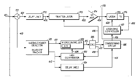
threshold 605. In other embodiments, the anti-clipping signal can be applied
for a
predetermined or dynamically determined duration after the peak of the power
envelope amplitude signal 413-2 is above the clipping threshold.
[0074] In scenario 630, while the peaks of the power envelope amplitude signal
413-3 indicates that the power envelope amplitude remains below the clipping
threshold 605, the RMS signal 411-3 indicates that the RMS power level is
above the
clipping threshold 605. In such scenarios, the anti-clipping circuit 170 does
not apply
the anti-clipping signal to the laser module, but it does attenuate the RF
input signal
sufficiently to reduce the RMS power level so that it is reduced to a level
below the
clipping threshold (e.g., Mode 3: attenuation on and anti-clipping bias off).
[0075] In scenario 640, peaks in the power envelope amplitude signal 413-4 and
the
RMS signal 411-4 indicate that the power envelope amplitude and RMS power
level
CA 02956317 2017-01-25
WO 2016/014935
PCT/US2015/041974
are above the clipping threshold 605. In such scenarios, the anti-clipping
circuit 170
can apply a corresponding level of attenuation to the RF input signal and
apply the
anti-clipping signal to the laser module (e.g., Mode 4: with attenuation on
and anti-
clipping bias off).
[0076] Particular embodiments may be implemented in a non-transitory computer-
readable storage medium for use by or in connection with the instruction
execution
system, apparatus, system, or machine. The computer-readable storage medium
contains instructions for controlling a microcontroller or computer system to
perform
a method described by particular embodiments. The microcontroller or computer
system may include one or more computing devices. The instructions, when
executed
by one or more computer processors or microcontrollers, may be operable to
perform
that which is described in particular embodiments.
[0077] As used in the description herein and throughout the claims that
follow, "a",
"an", and "the" includes plural references unless the context clearly dictates
otherwise. Also, as used in the description herein and throughout the claims
that
follow, the meaning of "in" includes "in" and "on" unless the context clearly
dictates
otherwise.
[0078] The above description illustrates various embodiments along with
examples
of how aspects of particular embodiments may be implemented. The above
examples
and embodiments should not be deemed to be the only embodiments, and are
presented to illustrate the flexibility and advantages of particular
embodiments as
defined by the following claims. Based on the above disclosure and the
following
claims, other arrangements, embodiments, implementations and equivalents may
be
employed without departing from the scope hereof as defined by the claims.
21