Note: Descriptions are shown in the official language in which they were submitted.
CA 02956504 2017-01-27
Description
Title of Invention: Vehicle Antenna Device
Technical Field
[0001]
The present invention relates to a vehicle antenna
device which is to be mounted, for example, on a roof of a
vehicle.
Background Art
[0002]
Recently, an antenna which is called a shark fin
antenna has been developed. The height of the antenna is
reduced, for example, to about 70 mm. On the other hand,
the length of the antenna is increased in order to ensure
the gain. Hence, the antenna base is larger as compared to
a prior art one. From the viewpoints of the weight
reduction and the cost reduction, therefore, a structure in
which the antenna base is made of a resin is proposed.
Patent Literature 1 below discloses a structure in which a
metal-made base is assembled to a resin-made base from an
inside of an antenna. In this structure, the size of the
metal-made base is set in accordance with a size of the
mounted antenna and the necessity/unnecessity of grounding
depending on a antenna system, and the base of an antenna
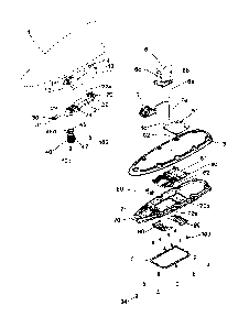
in which grounding is unnecessary is made of a resin,
1
CA 02956504 2017-01-27
whereby the metal-made base can be miniaturized as far as
possible.
Citation List
Patent Literature
[0003]
Patent Literature 1: JP-A-2012-204996
Summary of Invention
Technical Problem
[0004]
According to the structure in Patent Literature 1, in
the case where the resin-made base enters between the
metal-made base and the vehicle body (for example, the
roof), and an antenna for a broadband such as the LTE is
integrated, a phenomenon sometimes occurs in which the
metal-made base has a resonance point according to a
distance with respect to the vehicle body (ground), the
unwanted resonance is occurred in a required frequency band,
and then, the antenna gain is reduced.
[0005]
The present invention has been conducted in view of
such circumstances. It is an object of the present
invention to provide a vehicle antenna device in which a
reduction in the antenna gain can be avoided due to
unwanted resonance between a metal-made base and a vehicle
body.
2
CA 02956504 2017-01-27
Solution to Problem
[0006]
An aspect of the present invention is a vehicle
antenna device. The vehicle antenna device includes:
an antenna base;
an antenna case which is overlaid on the antenna base;
and
an antenna element and an amplifier board which are
disposed inside the antenna case,
the antenna base has a resin-made base which has an
opening, and a metal-made base which is smaller in area
than the resin-made base, is the metal-base being disposed
on the resin-made base so as to close the opening, and
having a cylindrical portion for attachment to a vehicle
body, and
a conductor plate is attached to a surface of the
resin-made base, the surface being opposite to a placement
surface of the metal-made base.
[0007]
The conductor plate may be electrically connected to
the metal-made base.
[0008]
In the conductor plate, as viewed in an axial
direction of the cylindrical portion, an outer edge
excluding a side facing a side of the cylindrical portion
3
CA 02956504 2017-01-27
may approximately coincide with an outer edge of the metal-
made base, or be outside the outer edge of the metal-made
base.
[0009]
The conductor plate may have at least one plate spring
portion which extends so as to approach the vehicle body.
[0010]
The conductor plate may be disposed respectively in
front and rear of the cylindrical portion.
[0011]
In the metal base, a resin-made part which prevents
the metal base from being directly contacted with an inner
circumferential portion of a mounting hole of the vehicle
body may be disposed in a portion opposed to the inner
circumferential portion of the mounting hole.
[0012]
The resin-made part may be a holder for provisionally
fixing the vehicle antenna device to the vehicle body.
[0013]
A boss which is engaged with the inner circumferential
portion of the mounting hole of the vehicle body may be
disposed on a surface of the resin-made base, the surface
being on a side of the vehicle body.
[0014]
4
CA 02956504 2017-01-27
The antenna element may include a capacitive element,
a coil element, and another antenna element for a frequency
band which is different from a frequency band received by
the capacitive element and the coil element.
[0015]
A shape and a size of the metal-made base may be set
so that, in a state where the conductor plate is absence,
unwanted resonance is generated in a vicinity of a lowest
frequency in a reception frequency band of the another
antenna element.
[0016]
A filter board may be disposed between the capacitive
element and the coil element.
[0017]
The coil element may be configured by forming a
winding around a bobbin,
a first terminal to which one end of the coil element
is electrically connected may be disposed on a side of one
end of the bobbin, and
a lower surface of the filter board may be in contact
with and electrically connected to the first terminal, and
an upper surface of the filter board may be in contact with
and electrically connected to the capacitive element.
[0018]
CA 02956504 2017-01-27
Connecting portions of the first terminal, the filter
board, and the capacitive element may be screwed to the
antenna case in a state where the connecting portions
overlap with one another, and electrically connected to one
another at the screwed portions.
[0019]
The vehicle antenna device may include an element
holder which supports the capacitive element and the coil
element, and
the element holder may have a placement portion on
which the filter board is to be placed.
[0020]
The placement portion may slidably support the filter
board, and the filter board is latched by a latching claw
at a predetermined slide position.
[0021]
Arbitrary combinations of the above-described
components, and expressions of the present invention which
are converted in method and system are also effective as
aspects of the present invention.
Advantageous Effects of Invention
[0022]
According to the present invention, it is possible to
provide a vehicle antenna device in which the reduction in
6
CA 02956504 2017-01-27
the antenna gain can be avoided due to the unwanted
resonance between the metal-made base and the vehicle body.
Brief Description of Drawings
[0023]
[Fig. 1] Fig. 1 is an exploded perspective view of a
vehicle antenna device according to an embodiment of the
present invention.
[Fig. 2] Figs. 2(A), 2(B) and 2(C) are external views of
the vehicle antenna device.
[Fig. 3] Fig. 3 is a side sectional view of the vehicle
antenna device.
[Fig. 4] Fig. 4 is a perspective view of the vehicle
antenna device in a state where conductor plates 90 are
disassembled, as seen from the lower side.
[Fig. 5] Fig. 5 is a perspective view of the vehicle
antenna device, as seen from the lower side.
[Fig. 6] Fig. 6 is an enlarged sectional view taken along
A-A in Fig. 2(C).
[Fig. 7] Figs. 7(A) to 7(D) are external views of a metal-
made base 60 in Fig. 1.
[Fig. 8] Figs. 8(A), 8(B) and 8(C) are external views of a
resin base 70 in Fig. 1.
[Fig. 9] Figs. 9(A), 9(B) and 9(C) are external views of
the conductor plate 90 in Fig. 1.
7
CA 02956504 2017-01-27
[Fia. 10] Fig. 10 is a perspective view of a disassembled
state of the metal-made base 60 and a provisional fixing
holder 80 of the vehicle antenna device.
[Fig. 11] Fig. 11 is a perspective view of an assembled
state of the metal-made base 60 and the provisional fixing
holder 80 in Fig. 10.
[Fig. 12] Figs. 12(A) and 12(B) are external views of the
vehicle antenna device in a state where the device is
attached to a through hole 111 of a vehicle body roof 110,
as seen from the lower side.
[Fig. 13] Fig. 13 is a perspective view of a disassembled
state of a bobbin 41, an upper terminal 45, and a lower
terminal 47 of a coil element 40 in Fig. 1.
[Fig. 14] Fig. 14 is a perspective view of an assembled
state of the bobbin 41, the upper terminal 45, and the
lower terminal 47 in Fig. 13.
[Fig. 15] Figs. 15(A) to 15(H) are views illustrating steps
of producing the coil element 40.
[Fig. 16] Fig. 16 Is a perspective view of an element
holder 20 in Fig. 1.
[Fig. 17] Fig. 17 is a plan view of the element holder.
[Fig. 18] Fig. 18 is a side view of the element holder.
[Fig. 19] Fig. 19 is a front view of the element holder.
[Fig. 20] Figs. 20(A), 20(B) and 20(C) are external views
of a filter board 30 in Fig. 1.
8
CA 02956504 2017-01-27
[Fig. 211 Figs. 21(A) and 21(B) are views illustrating
processes of attaching the filter board 30 to the element
holder 20.
[Fig. 22] Fig. 22 is a plan view of the element holder 20
which provisionally holds the filter board 30.
[Fig. 23] Fig. 23 is a sectional view taken along A-A in
Fig. 22.
[Fig. 24] Fig. 24 is an enlarged sectional view taken along
B-B in Fig. 22.
[Fig. 25] Figs. 25(A) and 25(B) are perspective views of
main portions of a vehicle antenna device according to a
comparison example, as seen from the lower side.
[Fig. 26] Fig. 26 is a characteristic graph of VSWR versus
frequency of vehicle antenna devices of an ideal state
where unwanted resonance does not occur, the embodiment,
and Comparison examples 1 and 2.
[Fig. 27] Fig. 27 is a characteristic graph in which the
vicinity of 700 MHz in Fig. 26 is enlarged.
Description of Embodiments
[0024]
Hereinafter, a preferred embodiment of the present
invention will be described in detail with reference to the
drawings. Identical or equivalent components, members, and
the like shown in the drawings are denoted by the same
reference numerals, and duplicated descriptions are
9
CA 02956504 2017-01-27
appropriately omitted. The embodiment does not limit the
invention, but only exemplifies the invention, and all
features described in the embodiments, and their
combinations are not necessarily essential in the invention.
[0025]
Fig. 1 is an exploded perspective view of a vehicle
antenna device according to the embodiment of the present
invention. Fig. 2(A) is a front view of the vehicle
antenna device. Fig. 2(B) is a side view of the vehicle
antenna device, and Fig. 2(0) is a bottom view of the
vehicle antenna device. Fig. 3 is a side sectional view of
the vehicle antenna device. Fig. 4 is a perspective view
of the vehicle antenna device in a state where conductor
plates 90 are disassembled, as seen from the lower side.
Fig. 5 is a perspective view of the vehicle antenna device,
as seen from the lower side. Fig. 6 is an enlarged
sectional view taken along A-A in Fig. 2(0). Fig. 7(A) is
a bottom view of a metal-made base 60 in Fig. 1. Fig. 7(B)
is a rear sectional view of the metal-made base, Fig. 7(C)
is a side view of the metal-made base, and Fig. 7(D) is a
side sectional view of the metal-made base. Fig. 8(A) is a
side sectional view of a resin base 70 in Fig. 1. Fig.
8(B) is a side view of the resin base, and Fig. 8(C) is a
bottom view of the resin base. Fig. 9(A) is a side view of
the conductor plate 90 in Fig. 1. Fig. 9(B) is a bottom
CA 02956504 2017-01-27
view of the conductor plate, and Fig. 9(C) is a rear view
of the conductor plate.
[0026]
An antenna case 1 is made of a radio wave transmissive
synthetic resin (a molded product made of a resin such as
PC or PET), and formed into a shark fin shape in which the
side surfaces are inwardly curved. An antenna base is
configured by combining the metal-made base 60 with the
resin-made base 70. The resin-made base 70 has through
holes 72a, 72b in a middle portion of a planar portion 71.
A pair of bosses (projections) 71a which is engaged with an
inner edge portion of a mounting hole of the vehicle body
is disposed on the lower surface (the surface on the side
of the vehicle body) of the planar portion 71. The metal-
made base 60 is smaller in area than the resin-made base 70,
and attached (fixed) by eight screws 103 onto the planar
portion 71 of the resin-made base 70 so as to close the
through holes 72a, 72b of the resin-made base 70. The
metal-made base 60 has: a planar portion 61 which is to
cover the through holes 72a, 72b; and a feeding cylindrical
portion (hollow threaded shaft portion) 62 which is
downwardly projected from the planar portion 61, and in
which a male thread for attachment to the vehicle body (for
example, the roof that is the panel to which attachment is
to be made) is formed on the outer circumference. Convex
11
CA 02956504 2017-01-27
portions 61a, 61b (Fig. 4) which are to be fitted into the
through holes 72a, 72b of the resin base 70 are disposed on
the lower surface of the planar portion 61. The feeding
cylindrical portion 62 extends from the convex portion 61a
toward the lower side of the resin-made base 70. An
amplifier board 50 is attached (fixed) by screwing or the
like onto the planar portion 61. A pair of conductor plate
springs (terminals) 51 is disposed on the amplifier board
50. An output cable 52 downwardly elongates from the
amplifier board 50, and passes through the inside of the
feeding cylindrical portion 62 so as to be drawn out to the
outside. An annular sealing member 5 is disposed between
the planar portion 71 of the resin-made base 70 and the
vehicle body. The sealing member 5 is disposed in the
periphery of the through holes 72a, 72b of the resin-made
base 70, and sandwiched and pressed between the planar
portion 71 of the resin-made base 70 and the vehicle body,
thereby preventing water from penetrating through a gap
between the resin-made base 70 and the vehicle body.
[0027]
A pad 3 is an elastic member made of elastomer, rubber,
or the like, and disposed on the resin-made base 70 so as
to make a circle along the periphery of the resin-made base
70 or the vicinity thereof. The pad 3 functions as a
blinder for the gap between the the lower end edge of the
12
CA 02956504 2017-01-27
antenna case 1 and the vehicle body, and has also a simple
waterproof function exerted between the resin-made base 70
and the vehicle body (the waterproof function is mainly
exerted by the sealing member 5). The antenna case 1 is
overlaid from the upper side on the resin-made base 70
while interposing the pad 3 between the antenna case 1 and
the resin-made base 70, and attached (fixed) by nine screws
104 to the resin-made base 70. The antenna case 1 has a
rib la (Fig. 3) for pressing the pad 3 against the whole
circumference of the resin-made base 70. Therefore,
penetration of water through a gap between the antenna case
1 and the resin-made base 70 can be avoided. Threaded-hole
equipped bosses lb, ic (Fig. 3) are disposed on the ceiling
portion of the antenna case 1. An LTE element 6, a
satellite radio antenna 7, a capacitive element 10, and a
coil element 40 which are antenna elements are disposed in
a space between the antenna case 1 and the antenna base
(the metal-made base 60 and the resin-made base 70). The
capacitive element 10 and the coil element 40 are elements
for an AM/FM antenna. The LTE element 6 and the satellite
radio antenna 7 are examples of antenna elements other than
elements for an AM/FM antenna.
[0028]
The LTE element 6 is configured by a metal plate
(conductor plate), and supported by a holder 6c which is
13
CA 02956504 2017-01-27
erected from a board 6b. The board 6b is attached (fixed)
by screwing or the like onto the planar portion 61 of the
metal base 60. An output cable 6a elongates from the board
6b, and passes together with the output cable 52 of the
amplifier board 50 through the inside of the feeding
cylindrical portion 62 so as to be drawn out to the outside.
The satellite radio antenna 7 is disposed on the planar
portion 71 of the resin base 70. An output cable 7a of the
satellite radio antenna 7 passes together with the output
cable 6a of the LTE element 6 through the inside of the
feeding cylindrical portion 62 so as to be drawn out to the
outside.
[0029]
The capacitive element 10 is configured by a metal
plate (conductor plate), and bent in, for example, a
squeezing process so as to have an umbrella-shaped curved
surface portion 11 which is approximately parallel to an
arcuate ceiling surface that is in the upper portion of the
inside of the antenna case 1. In a state where the
capacitive element 10 is fixed to the antenna case 1, the
curved surface portion 11 is in proximity to the ceiling
surface of the antenna case 1. A connecting portion 12
extends downwardly and rearwardly from a front end portion
of the curved surface portion 11, to be formed into an L-
like shape. The connecting portion 12 has a through hole
14
CA 02956504 2017-01-27
13 (Fig. 3) in a tip end portion. The upper surface of the
periphery of the through hole 13 of the connecting portion
12 butts against the end surface of the threaded-hole
equipped boss lb (Fig. 3) in the antenna case 1. The lower
surface of the periphery of the through hole 13 of the
connecting portion 12 butts against the upper surface side
of a conduction pattern 31a of a filter board 30 which will
be described later. The lower surface side of the
conduction pattern 31a of the filter board 30 butts against
an upper terminal 45 of the coil element 40. In the curved
surface portion 11, a through hole 14 (Fig. 1) is disposed
in the rear side. The threaded-hole equipped boss lc (Fig.
3) of the antenna case 1 is passed through the inside of
the through hole 14.
[0030]
An element holder 20 has a base portion 21, a
cylindrical portion 22, a through hole 23, and a placement
portion 24. The cylindrical portion 22 is raised from the
base portion 21. The threaded-hole equipped boss lc of the
antenna case ] is fitted into the inside of the cylindrical
portion (Fig. 3). The element holder 20 is attached
(fixed) to the antenna case 1 while interposing the
capacitive element 10 between the element holder 20 and the
antenna case 1, by a screw 102 which is screwed to the
threaded-hole equipped boss lc. Projections 22a are
CA 02956504 2017-01-27
disposed in front and rear of the cylindrical portion 22,
respectively. The projections 22a press the capacitive
element 10 against the ceiling surface of the antenna case
1. The through hole 23 is disposed in the base portion 21,
and located in front of the cylindrical portion 22. The
element holder 20 has a space in which an upper portion of
a bobbin 41 of the coil element 40 that will be described
later is positioned and supported (fitted), below the
through hole 23. The periphery and rear of the through
hole 23 of the base portion 21 are formed as the placement
portion 24 on which the filter board 30 is to be placed.
The placement portion 24 will be described later. The
filter board 30 is slid from the front side to be attached
(provisionally fixed) to the placement portion 24.
[0031]
As shown in Fig. 3, the coil element 40 is configured
by forming a winding 42 around the bobbin 41 which is made
of a resin. The upper terminal 45 is disposed (for example,
pressingly inserted and fixed) in one end (upper end) of
the bobbin 41. One end of the winding 42 is electrically
connected to the upper terminal 45. A lower terminal 47 is
disposed (for example, pressingly inserted and fixed) in
the other end (lower end) of the bobbin 41. The other end
of the winding 42 is electrically connected to the lower
terminal 47. The upper terminal 45 is attached (fixed) to
16
CA 02956504 2017-01-27
the threaded-hole equipped boss lb of the antenna case 1
while interposing the filter board 30 (conduction pattern
31a) and the connecting portion 12 of the capacitive
element 10 between the upper terminal 45 and the antenna
case 1, by a screw 101. Namely, the screw 101 passes
through a through hole 45d of the upper terminal 45, a
through hole 31 of the filter board 30, and the through
hole 13 of the connecting portion 12 of the capacitive
element 10, and is screwed to the threaded-hole equipped
boss lb of the antenna case 1. Therefore, the coil element
40 and the capacitive element 10 are electrically connected
to each other, and the filter board 30 is electrically
connected between the coil element 40 and the capacitive
element 10. Preferably, the screw 101 may have a spring
washer so as to avoid a connection failure due to its ,
loosening. A connection leg 47b of the lower terminal 47
is clamped by a pair of conductor plate springs 51 of the
amplifier board 50. Therefore, the coil element 40 and the
amplifier board 50 are electrically connected to each other.
[0032]
In the planar portion 71 of the resin base 70, two
conductor plates 90 are attached (fixed) to the surface
(lower surface) opposite to a placement surface (upper
surface) of the metal-made base 60, by eight screws 103.
One of the conductor plates 90 is located in front of the
17
CA 02956504 2017-01-27
feeding cylindrical portion 62, and the other conductor
plate 90 is located in rear of the feeding cylindrical
portion 62. The outer edge (three sides excluding a side
facing the feeding cylindrical portion 62) of each of the
conductor plates 90 is in proximity to the inner edge of
the sealing member 5, and approximately coincides with the
outer edge of the metal-made base 60 as seen in the axial
direction (vertical direction) of the feeding cylindrical
portion 62. As shown in Fig. 4, each of the conductor
plates 90 has a screwed portion 93 in each of four corners
of a corresponding planar portion 91. Each of the screwed
portions 93 has a through hole 93a through which the
corresponding screw 103 is passed, and is bent into an L-
like shape so as to be raised to be higher than the planar
portion 91 by one step. By contrast, eight concave
portions 73 into which the screwed portions 93 of the
conductor plates 90 enter respectively are disposed on the
lower surface of the planar portion 71 of the resin base 70.
A through hole 73a through which the screw 103 passes is
disposed in each of the concave portions 73. The screws
103 cause the conductor plates 90 to be attached to the
lower surface of the resin base 70, and the metal-made base
60 to be attached to the upper surface of the resin base 70.
The metal-made base 60 and the conductor plates 90 are
electrically connected to each other by the screws 103.
18
CA 02956504 2017-01-27
Each of the conductor plates 90 has four plate spring
portions 92 which are bent in an obliquely downward
direction from the planar portion 91 so as to approach the
side of the vehicle body. Tip end portions of the plate
spring portions 92 face the side of the feeding cylindrical
portion 62, and are contacted with the vehicle body roof
(compressed by the vehicle body roof).
[0033]
Fig. 10 is a perspective view of a disassembled state
of the metal-made base 60 and the provisional fixing holder
80 of the vehicle antenna device. Fig. 11 is a perspective
view of an assembled state of the metal-made base 60 and
the provisional fixing holder 80 in Fig. 10. Fig. 12(A) is
a perspective view of a state where the vehicle antenna
device is attached to a through hole 111 of the vehicle
body roof 110, as seen from the lower side. Fig. 12(B) is
a bottom view of the state. The provisional fixing holder
80 which serves as the resin-made part has a U- or C-shaped
external shape, and is engageable with (fittable into) the
side surface of the feeding cylindrical portion 62 in a
lateral direction perpendicular to the axial direction
thereof. The provisional fixing holder 80 provisionally
fixes the feeding cylindrical portion 62 in a state where
the feeding cylindrical portion is inserted from the
outside into the through hole 111 of the vehicle body roof
19
CA 02956504 2017-01-27
110 that serves as the panel to which attachment is to be
made. The provisional fixing holder 80 is made of, for
example, a flexible resin, and has: a pair of clamping
portions 81 which clamps the feeding cylindrical portion
62; a liaison portion 82 through which the clamping
portions 81 are connected to each other; and latching claws
83 which are formed in tip end portions of the clamping
portions 81, respectively, so as to be outwardly projected.
The feeding cylindrical portion 62 has on the side surface
a pair of first groove portions 63 (Figs. 7(B) and 10)
which is engaged with the provisional fixing holder 80, and
one second groove portion 64 which is at the midpoint
between the first groove portions 63. The provisional
fixing holder 80 is attached to the feeding cylindrical
portion 62 by being engaged with the first groove portions
63 and the second groove portion 64. Namely, the pair of
clamping portions 81 is engaged with the pair of first
groove portions 63 so as to sandwich the feeding
cylindrical portion 62, and the liaison portion 82 is
engaged with the second groove portion 64. In the state
where, after the provisional fixing holder 80 is attached
to the feeding cylindrical portion 62, the feeding
cylindrical portion 62 is inserted into the through hole
111 of the vehicle body roof 110, the latching claws 83 are
caught by the inner surface of the roof, and can function
CA 02956504 2017-01-27
as the provisionally fixation. As shown in Figs. 12(A) and
12(3), the provisional fixing holder 80 which is made of a
resin is interposed between the feeding cylindrical portion
62 and an inner edge portion (inner circumferential
portion) of the through hole 111 of the vehicle body roof
110 to prevent the both members from being directly
contacted with each other, i.e., from being electrically
connected to each other.
[0034]
Fig. 13 is a perspective view of a disassembled state
of the bobbin 41, the upper terminal 45, and the lower
terminal 47 of the coil element 40 in Fig. 1. Fig. 14 is a
perspective view of an assembled state of the bobbin 41,
the upper terminal 45, and the lower terminal 47 in Fig. 13.
Figs. 15(A) to 15(H) are views illustrating steps of
producing the coil element 40.
[0035]
The upper terminal 45 has a base portion 45a, a pair
of attaching legs 45b, and a winding terminal connecting
portion (tab) 45c. A through hole 45d is disposed in a
middle portion of the base portion 45a. The pair of
attaching legs 45b is bent into a U-like shape with respect
to the base portion 45a, and located in the opposite sides
across the center of the base portion 45a, respectively.
The winding terminal connecting portion 45c is bent into an
21
CA 02956504 2017-01-27
L-like shape with respect to the base portion 45a, and
located in a different position which is rotated by 90
degrees in an axial direction from the attaching legs 45b.
[0036]
The lower terminal 47 has an upper surface portion 47a,
a connection leg 47b, a winding terminal connecting portion
(tab) 47c, side surface portions 47e, and a lower surface
portion 47f. A plate spring portion 47d which is bent in
an obliquely downward direction is disposed in a middle
portion of the upper surface portion 47a. The plate spring
portion 47d has a function of preventing the bobbin 41 from
rattling with respect to a lower terminal attaching portion
44 of the bobbin 41. The connection leg 47b is downwardly
bent with respect to the base portion 45a. The winding
terminal connecting portion 47c extends from the upper
surface portion 47a to be projected toward the outside.
The side surface portions 47e are downwardly bent with
respect to the upper surface portion 47a at the both ends
of the upper surface portion 47a, respectively. The lower
surface portion 47f is a portion which is formed by bending
the lower end of one of the side surface portions 47e, and
extending the lower end approximately in parallel to the
upper surface portion 47a. The lower terminal 47 is
attached to the lower terminal attaching portion 44 in such
a manner that the lower terminal attaching portion 44 is
22
CA 02956504 2017-01-27
surrounded by the upper surface portion 47a, the side
surface portions 47e, and the lower surface portion 47f.
[0037]
The bobbin 41 has: upper terminal attaching portions
43 to which the upper terminal 45 is to be attached; the
lower terminal attaching portion 44 to which the lower
terminal 47 is to be attached; and a cylindrical winding
barrel 48 in which the winding 42 is wound on the outer
circumferential surface. The upper terminal attaching
portions 43 are erected on the upper end surface of the
winding barrel 48 while being distributed on the both sides
of the center axis of the winding barrel 48. The upper
terminal attaching portions 43 have a pair of convex
portions 43a which is outwardly projected in the opposite
directions to each other. The pair of convex portions 43a
is engaged with the pair of attaching legs 45b of the upper
terminal 45. The lower terminal attaching portion 44 is
disposed so as to protrude toward the outside in the lower
end portion of the winding barrel 48. A guide groove 48a
which is the winding path of the winding 42, and a
plurality of projections 48b which are in positions along
the winding path of the winding 42 are disposed on the
outer circumferential surface of the winding barrel 48.
The guide groove 48a spirally extends around the outer
circumferential surface of the winding barrel 48. At least
23
CA 02956504 2017-01-27
one of the projections 48b is disposed in each of a
plurality of circumferential positions (circumferential
positions where the later-described winding terminal
connecting portion 45c of the upper terminal 45 can exist)
on the outer- circumferential surface of the winding barrel
48. In the illustrated example, the projections 48b are
disposed in two circumferential positions which are
separated from each other by 180 degrees, and which are on
the outer circumferential surface of the winding barrel 48,
in plural numbers (ten in one of the positions, and eleven
in the other position). One of the circumferential
positions where the projections 48b are disposed coincides
with the circumferential position of the winding terminal
connecting portion 45c of the upper terminal 45. Each of
the projections 48b functions as a hooking portion in the
case where the winding end portion of the winding 42 is
drawn out in the axial direction. From the viewpoint of
ensuring of strength, the projections 48b are formed into a
planer shape.
[0038]
As shown in Figs. 15(A) and 15(3), when the coil
element 40 is to be assembled, first, the upper terminal 45
and the lower terminal 47 are slidingly attached to the
upper terminal attaching portions 43 and the lower terminal
attaching portion 44 of the bobbin 41, respectively. As
24
CA 02956504 2017-01-27
shown in Fig. 15(C), then, a bent end portion of a wire 42'
which is to be configured as the winding 42 is hooked to
the winding terminal connecting portion 47c of the lower
terminal 47, and connected and fixed thereto by soldering,
welding, or the like. As shown in Figs. 15(D) and 15(E),
then, the winding 42 is wound around the outer
circumferential surface (guide groove 48a) of the winding
barrel 48 of the bobbin 41, while rotating the bobbin 41.
The winding pitch of the winding 42 is determined by the
arrangement pitch of the guide groove 48a. As shown in
Figs. 15(F), 15(G), and 15(H), then, the winding end
portion of the winding 42 is hooked on the predetermined
projection 48b of the winding barrel 48, the terminal of
the winding 42 is drawn out in the axial direction, the
terminal of the winding 42 is connected and fixed to the
winding terminal connecting portion 45c of the upper
terminal 45 by soldering, welding, or the like, and an
excess portion is cut away. The above-described series of
operations can be conducted by an automatic winding machine.
As a result, the coil element 40 is completed. The coil
element 40 is installed into the antenna case 1 in
following manner. First, the upper terminal 45 is fixed
together with the capacitive element 10 to the threaded-
hole equipped boss lb of the antenna case 1 by the screw
101. Then, the connection leg 47b of the lower terminal 47,
CA 02956504 2017-01-27
and the conductor plate springs 51 of the amplifier board
50 are positioned relative to each other, and an assembly
of the amplifier board 50, the metal-made base 60, and the
resin-made base 70 is attached to the antenna case 1 by,
for example, screwing. Alternatively, the upper terminal
45 may be attached while being inverted by 180 degrees with
respect the bobbin 41. When the projection 48b on which
the winding end portion of the winding 42 is to be hooked
is changed, and, as required, the upper terminal 45 is
inverted by 180 degrees, the number of turns of the winding
42 can be changed in units of 0.5 turn.
[0039]
Fig. 16 is a perspective view of the element holder 20
in Fig. 1. Fig. 17 is a plan view of the element holder 20.
Fig. 18 is a side view of the element holder 20, and Fig.
19 is a front view of the element holder 20. Fig. 20(A) is
a plan view of the filter board 30 in Fig. 1. Fig. 20(B)
is a side view of the filter board 30, and Fig. 20(C) is a
bottom view of the filter board 30. Figs. 21(A) and 21(B)
are views illustrating processes of attaching the filter
board 30 to the element holder 20. Fig. 22 is a plan view
of the element holder 20 which provisionally holds the
filter board 30. Fig. 23 is a sectional view taken along
A-A in Fig. 22. Fig. 24 is an enlarged sectional view
taken along B-B in Fig. 22.
26
CA 02956504 2017-01-27
[0040]
The element holder 20 has the placement portion 24 on
which the filter board 30 is to be placed. Latching claws
24b are disposed on the both sides of the placement portion
24, respectively. A pair of projecting portions 24a is
inwardly projected from the both upper sides of the through
hole 23, respectively. The filter board 30 has a pair of
cutouts 35 in the right and left sides. In the case where
the filter board 30 is to be provisionally fixed to the
placement portion 24 of the element holder 20, the filter
board 30 is placed from the upper side on the placement
portion 24 as shown in Fig. 21(A) while locating the
cutouts 35 at the positions of the projecting portions 24a.
The filter board 30 is rearwardly slid until butting occurs
as shown in Fig. 21(B). Then, the pair of latching claws
24b is engaged with the edge portions of the cutouts 35 to
latch (provisionally fix) the filter board 30. Moreover,
the upper surface of the filter board 30, and the pair of
projecting portions 24a and a pair of projecting portions
24c are engaged (face-to-face contacted) with each other,
and the filter board 30 is prevented from upwardly slipping
off. The filter board 30 has the conduction pattern 31a on
the both surfaces of the periphery of the through hole 31,
an inductive pattern 32a on the upper surface, and an
inductive pattern 32b on the lower surface. The inductive
27
CA 02956504 2017-01-27
patterns 32a, 32b extend from the conduction pattern 31a,
and are connected to each other by a through hole 34. A
chip capacitor 33 is disposed in the middle of the
inductive pattern 32a.
[0041]
Fig. 25(A) is a perspective view of main portions of a
vehicle antenna device according to Comparison example 1,
as seen from the lower side. Fig. 25(B) is a perspective
view of main portions of a vehicle antenna device according
to Comparison example 2, as seen from the lower side.
Comparison example 1 shown in Fig. 25(A) is a device of the
conventional type in which the conductor plates 90 in the
embodiment are not disposed, and a holder 880 for
provisional fixing to the vehicle body is attached from the
upper side of a metal base 860, and which is not provided
with a configuration for preventing the vehicle body roof
and the metal-made base 860 from being directly contacted
with each other. By contrast, Comparison example 2 shown
in Fig. 25(3) has the conductor plates 90 in the embodiment,
but, similarly with Comparison example 1, is not provided
with a configuration for preventing the vehicle body roof
and a metal-made base 960 from being directly contacted
with each other.
[0042]
28
CA 02956504 2017-01-27
Fig. 26 is a characteristic graph of VSWR versus
frequency of vehicle antenna devices according to an ideal
state where unwanted resonance does not occur, the
embodiment, and Comparison examples 1 and 2. Fig. 27 is a
characteristic graph in which the vicinity of 700 MHz in
Fig. 26 is enlarged. The first and second frequency bands
shown in these drawings are frequency bands used in the LTE.
In the case of the second frequency band, in any
configuration, characteristics which are close to the
characteristic according to the ideal state are obtained.
In the case of the first frequency band, in the
configurations of Comparison examples 1 and 2, by contrast,
the characteristics are largely deviated from the
characteristic according to the ideal state as enlargedly
shown in Fig. 27. In the configuration of the embodiment,
on the other hand, the characteristic is relatively close
to the characteristic according to the ideal state. The
characteristic according to the embodiment which is close
to the characteristic according to the ideal state is
attained by the effect because of a phenomenon in which the
capacitance is increased by the interposition of the
conductor plate 90 between the metal-made base 60 and the
vehicle body roof, and the resonance frequency is shifted
to a frequency band that is lower than the first frequency
band, and by the effect because of the configuration in
29
CA 02956504 2017-01-27
which direct contact between the metal-made base 60 and the
inner circumference of the mounting hole of the vehicle
body roof is avoided by the provisional fixing holder 80
(the effect because of the fact that an unintended
conduction path is not formed). In the configuration in
the embodiment, characteristics in a band (300 MHz to 400
MHz) which is not in the first and second frequency bands
are largely deviated from the characteristic according to
the ideal state. However, this is no problem since this
band is not used. In other words, according to the
configuration in the embodiment, the frequency band in
which deviation of the VSWR occurs due to unwanted
resonance is shifted into an unused band, whereby the VSWR
in the used frequency band can be made close to the VSWR in
the ideal state (a reduction in the antenna gain is
prevented).
[0043]
The shape and the size of the metal-made base 60 in
the embodiment is designed so that, in a state where a
countermeasure against unwanted resonance is not taken as
in Comparison example 1, unwanted resonance is generated in
the vicinity of the lowest frequency in a frequency band
which is used in the LTE as shown in Fig. 26. In an actual
design, also the size of the board 50 to be placed on the
metal-made base 60 is considered, the length of the metal-
CA 02956504 2017-01-27
made base 60 which has a rectangular shape, in the short-
side direction is first determined in accordance with the
size of board, and then the length in the long-side
direction is determined so that unwanted resonance is
generated in the vicinity of the lowest frequency in the
reception frequency band.
[0044]
According to the embodiment, it is possible to attain
the following effects.
[0045]
(1) The conductor plates 90 in the resin-made base 70 are
disposed on the surface opposite to the placement surface
of the metal-made base 60. Therefore, it is possible to
avoid the reduction in the antenna gain since unwanted
resonance due to an event that the metal-made base 60 has a
resonance point according to the distance with respect to
the vehicle body roof (ground) is occurred in a required
frequency band.
[0046]
(2) Since the conductor plates 90 have the plate spring
portions 92, and the plate spring portions 92 are
compressed by the vehicle body roof, the plate spring
portions 92 and the vehicle body roof can be surely
contacted with each other even when the curvature of the
31
CA 02956504 2017-01-27
vehicle body roof is changed, and therefore the reduction
in the antenna gain is surely avoided.
[0047]
(3) Since each of the plate spring portions 92 is branched
into a plurality of sections, many contacts can be ensured
even when the curvature of the vehicle body roof is large.
[0048]
(4) Since the filter board 30 is disposed between the
capacitive element 10 and the coil element 40, an adverse
influence due to interferences between the antenna elements
in the antenna case 1 can be reduced. Specifically, it is
possible to avoid the reduction in the antenna gain of the
LTE element 6 by a phenomenon that the second- or third-
harmonics of the capacitive element 10 and the coil element
40 (AM/FM) enter the LTE element 6.
[0049]
(5) The filter board 30 has the configuration where the
filter board 30 is fixed by the screw 101 in the state
(stacked stated) where the filter board 30 is sandwiched
between the upper terminal 45 of the coil element 40 and
the connecting portion 12 of the capacitive element 10, and
the filter board 30 is electrically connected between the
capacitive element 10 and the coil element 40 by the
screwing. Therefore, the mechanical fixation and the
electrical connection of the filter board 30 can be
32
CA 02956504 2017-01-27
performed in a lump and easily, and the assemblability is
excellent..
[0050]
(6) Since the element holder 20 has the configuration where
the element holder 20 has the placement portion 24 on which
the filter board 30 is to be placed, and the filter board
30 is provisionally fixed to the predetermined position by
the latching claws 24b and the projecting portions 24a, 24c,
positioning of the filter board 30 is not required in the
assembling process, and the assemblability is excellent.
[0051]
(7) The metal-made base 60 is formed into a size and shape
in which, in a state where a countermeasure against
unwanted resonance is not taken, unwanted resonance is
generated in the vicinity of the lowest frequency in the
reception frequency band. Therefore, the conductor plates
90 are disposed to cause unwanted resonance to be shifted
into a lower frequency band, whereby the position of
unwanted resonance can be surely deviated from the
reception frequency band.
[0052]
Although the present invention has been described with
reference to the embodiment, it is obvious to those skilled
in the art that the components and processing processes in
the embodiment can be variously modified within the scope
33
CA 02956504 2017-01-27
of the claims. Hereinafter, modifications will be
described.
[0053]
Even when each of the conductor plates 90 is
configured by a flat plate having no plate spring portions
92, a certain level of effects can be attained in
prevention of reduction of the antenna gain. Even when the
conductor plates 90 are not conductive with the metal-made
base 60, a certain level of effects can be attained in
prevention of reduction of the antenna gain. The outer
edge (three sides excluding the side facing the feeding
cylindrical portion 62) of each of the conductor plates 90
may be outside the outer edge of the metal-made base 60 as
seen in the axial direction (vertical direction) of the
feeding cylindrical portion 62.
Reference Signs List
[0054]
1 antenna case, la rib, lb, lc threaded-hole equipped
boss, 3 pad, 5 sealing member, 6 LTE element, 6a output
cable, 6b board, 6c holder, 7 satellite radio antenna,
7a output cable, 10 capacitive element, 11 curved
surface portion, 12 connecting portion, 13, 14 through
hole, 20 element holder, 21 base portion, 22 cylindrical
portion, 22a projection, 23 through hole, 24 placement
portion, 24a projecting portion, 24b latching claw, 24c
34
CA 02956504 2017-01-27
projecting portion, 30 filter board, 31 through hole, 31a
conduction pattern, 32a, 32b inductive pattern, 33 chip
capacitor, 34 through hole, 35 cutout, 40 coil element,
41 bobbin, 42 winding, 42' wire, 43 upper terminal
attaching portion, 43a convex portion, 44 lower terminal
attaching portion, 45 upper terminal (first terminal), 45a
base portion, 45b attaching leg, 45c winding terminal
connecting portion (tab), 45d through hole, 47 lower
terminal (second terminal), 47a upper surface portion, 47b
connection leg, 47c winding terminal connecting portion
(tab), 47d plate spring portion, 47e side surface portion,
47f lower surface portion, 48 winding barrel, 48a guide
groove, 48b projection, 50 amplifier board, 51 conductor
plate spring (terminal), 52 output cable, 60 metal-made
base (conductive base), 61 planar portion, 61a, 61b
convex portion, 62 feeding cylindrical portion (hollow
threaded shaft portion), 63 first groove portion, 64
second groove portion, 65 threaded hole, 70 resin-made
base (insulative base), 71 planar portion, 71a boss
(projection), 72a, 72b through hole, 73 concave portion,
73a through hole, 80 provisional fixing holder, 81
clamping portion, 82 liaison portion, 83 latching claw,
90 conductor plate, 91 planar portion, 92 plate spring
portion, 93 screwed portion, 93a through hole, 101, 102,
103, 104 screw